Note: Descriptions are shown in the official language in which they were submitted.
DYNAMI C SYSTEM ANALYS I S IN .A VI BRAT I NG
BEAII ACCELEROMETEP~
~3ACE~GROUND OF THE INVENTION
5 1. Field of Invention
The present invention relates to circuitry for analyzing
a dynamic system and more particularly to the
application of this circuitry to a vibrating beam
accelerometer ("VBA"). The circuitry analyzes a pair of
frequencies which are related to natural frequency as a
function of a force applied to a VBA to approximate
S t21 ( ~ f f)dt
2. Description of the Related Art
The term "system" is defined as an assemblage of objects
united by some form of interaction or interdependence.
For a dynamic system, ~here is the added restriction
that the interaction or interdependence will vary with
time. This dynamic behavior has been characterized by
observing certain relationships, including the
relationship between frequency and natural frequency-
(1) W = Wn (1 + KT) /2
~'7~6~)
where W is a frequency, Wn is a natural Erequeney, K is a
constant, and T is a force, for e~ample, -the tension o-E a
vibratin~ beam. The eharacterizations of the variables are
typical in the mechanical engineering arts. The equation has
been applied -to a wide range of dynamic systems, and a basic
description of this phenomenon can be found in Norman H. Beachley
and Howard L. Harrison, Introduction to Dynamic Systems (1978),
As applied in a VBA, the difference in two frequencies is
used to compute T, which is then used to caleulate acceleration
and velocity. For example, acceleration may be defined as being
equal to the constant K times the difference in two frequeneies
( Wl~W2 ) -
In designing cireuitry to analyze the relationships in equation
1, a fundamental problem has been the non-linear nature of the
equation. It has always been assumed that the effects of this
non-linearity could be overcome by using a computer to make
linear ealculations and then to eompensa-te for the error eaused
by the non-linearity. However, the presenee of high levels of
vibration produces a strong bias whieh normally makes computer
compensation difficult and unreliable. This is true because the
bias is determined by the harmonic conten-t of the vibration and
computer itera-tion is slow compared to higher vibration
frequeneies.
In prac-tical applieations sueh as a VBA, the presenee o very
high levels of vibration, severe aeeeleration and the non-
linearity causes a large statie error in the acceleration output.
This acceleration error cannot be reduced by computer correetion
for eases where the vibration frequeney is greater than one-half
the eomputer sampling frequency. If the vibration level is
separately observed and its wave-shape is known, correction is
possible. However, this approach would appear to require the use
of a plurality of additional
~271~60
-- 3
accelerometers for sensing. Thus, the applications of such
aynamic system analysis circuitry have been severely limited.
SUMMARY OF THE INVENTION
~ . _
It is an aspect oE one embodimen-t of the present inVention to
provide an apparatus and a method for more accurately analyzing
the above relation~hipsO
According to one embodiment of the present invention there is
provided an apparatuQ for analy~ing a pair of frequencies which
are related to natural frequency as a ~unction of a ~orce applied
to a system, the system including means producing a first
frequency (fl) and a second frequency (f2) comprising: means ~or
sensing the first frequency (fl) and the second frequency (f2);
means for squaring the first and second frequencies to produce
fl2 and f22, respectively; means for computing the dif~erence
between the squared frequencies (fl2-f223 to approximateSt1(~f ~f)dt
to obtain a measure of the force applied to the system.
According to another embodiment of the present invention there is
provided a method for analyzing a pair of frequencies which are
related to natural frequency as a function of force applied to a
system, the system including means producing a first frequency
~fl) and a second frequency (f2), comprising the steps of:
sensing the first frequency (fl) and the second frequency (f2)
squaring the first and second frequencies to produce fl2 and f22,
respectively; computing the difference between the squared
frequencies (fl2-f22) to approximate ~tl~f-~fldt
to obtain a measure of the force applied to the system.
Although the application of this circuitry is considerably
broader than i~s use in a VBA, this application is used to teach
7~
a best mode and manner o~ implementing of the invention.
A VBA is comprised of two beams. Each beam is located between a
mounting and, typically, a pendulous mass. The beams are
oriented in opposing directions. The beams are comprised o a
piezo electric material, for example quartz, which produces a
mechanical stress when subjected to a voltage. A vol-tage is
pulsed to each quartz beam to produce an oscillation. Moving the
VBA in a direction corresponding to the length of the beams
affec-ts -the pendulous mass, causing a change in the oscillations.
These changes are measured and used to compute acceleration.
As to general applications involving equation 1, the threshold
problem is to linearize a relationship which is typically
analyzed as a non-linear problem. By squaring equation (1) and
analyzing two ~requencies Wl and W2 corresponding to the two
beams with Kl and K2 constants that reflect the opposing
orientations, there are the following equations:
(2) = W12 = Wln2(1~KlT)
(3) = W22 = Wln2(1-K2T)
These equations can be combined to determine the force T as the
difference be-tween the squares of the frequencies~
(4) W12-W22 = Wln2-~Wln2KlT-W2n2-~W2n21~2T
( ) (Wln ~W2n )~(wln2Kl-~w2n2K2)T
This equation can be simplified and put into a forma-t for
determining force T from the change in frequencies.
(6) W12~W22 = A+BT
Solving for ~orce T, there is
(7) [(W12-W22)/B]+L-A/B] = T
Though not rigorously true as a linear equation, in most
applications, the relationship is sufficiently linearized to
allow the relationship to be implemented in circuitr~. In
equation (7), the [(W12-W22)/B] term may be represented in a
binomial expansion. The [-A/B] term indicates the bias because
.. . . . .
~ 5 --
quantity B is a s~ale factor and quantity A i8 a bia~.
More specifically, to apply this approach in a VBA, the present
invention can be unders-tood as obse.rving that the VBA is a linear
instrument in terms of the sum and difference frequency rather
than tne difference frequency currently employed in the prior
art. The VBA frequency output is analyzed by detecting, either
separately or in combination, the phase changes resulting from
these frequencies in a fixed time interval. Since phase is the
time integral of frequency, the output data provides a quasi-
function of the time integral of acceleration, or a quasi-
velocity. In terms of conventional instrumentation, the VBA is
capable of providing as its outputs:
~t2 f dt; ~t2 f dt;
(10) ~tl (fl-f2)dt; (11) ~tt21 (fl~f2)dt
where f is frequency and the particular characterizations of the
variables are typical of electrical engineering ar-ts.
Essentially, though, f corresponds to W in equation (1), etc.
Because only two independent data items are provided, any two of
the above outputs comple-tely define all four of the above
outputs. Thus, -the following outputs will be considered to be
the integral of the sum frequency and the integral of the
difference frequency:
~~ (13~ 5 tl ~fdt
Because a VBA is linear in terms of the product of the sum and
difference frequencies, what is desired is an output:
(14) ~t2 (~ f-~f~dt
Unfortunately, it is impossible to evaluate this integral based
upon the available integrals of the sum and difference
frequencies under conditions where f and ~ f, respectively, are a
function of time.
(15) ~ttl (~f-~f)dt ~ f(~ttl~fdt, 5tl ~ fdt)
The only way in which the required integral can be evaluated is
by multiplying ~f and f together prior to integration.
It would be ideal if an analog means existed for directly
multiplying two frequencies, similar to the means ~mixer) which
is used to add or subtract two frequencies. However, it will
suffice to evaluate ~ f and ~f at rates sufficiently above the
highest frequency of vibration so that it may be assumed that ~f
and ~f are constant for the sampling frequency. In ~his case,
the following relationship will hold to sufficient accuracy.
(16) Sttl ~f-~fdt~hf-~f ~tl dt
It is assumed that if the evaluation rate is higher than the
Nyquist frequency for the highest vibration component, accurate
results will be achieved.
Placing this VBA application in general perspective:
(17) f -(fl-f2) (fl~f2)
2 2 '
18~ f= f1 -f2 ~ A~BT
7~
because W = f in equation (6).
The present invention may be implemented in a VBA by de-termining
the individuial beam frequencies, dividing each cycle into
portions by means of a phase locked loop and determining the
number o portions of a cycle which occur in a fixed time
interval, as a digital number. The resultant digital number is
squared in a digital mul-tiplier and the squared numbers from the
two beams are subtracted to provide the output. Roundof~ loss
occurring in the digitization process are added to the next
sample of data, to ensure that there is no cumulative error.
BRIEF DESCRIPTION OF THE DRAWINGS
FIG. 1 is a circuit block diagram of a phase counter for a VBA.
FIG. 2 is control circuitry for a linearized VBA.
FIG. 3 is a timing diagram~
FIG. 4 is a schematic representation of a conventional two-beam
single axis vibra-ting beam accelerometer.
DETAI~ED DESCRIP~ION OF THE INVENTION
AND ITS PREFERRED EMBODIMENT
The present invention is disclosed in the context of a three-axis
system, i.e., X, Y and Z axes. For each axis there are then two
vibrating beams.
Referring to FI~. 4, there is shown a conventional prior art
vibrating beam accelerometer 100 which is housed in an enclosure
111. Within the enclosure 111, there are two independent
vibrating beam transduceris 112 and 117 mounted in opposition to
each other to achieve siymmetry and to permit cancellation of
~L~7~
-- 8 --
first order errors. A first section of the accelerometer
comprises the quar-tz crystal beam 112 and the pendulous mass 113
supported for movement about flexure hinge 114 which in turn is
connected -to the mounting surEace 116. A second section of the
accelerometer comprises the quartz crystal beam 117 and the
pendulous mass 118 supported for movement about flexure hinge 119
which in turn is connected to the mounting surface 120. Each
pendulous mass i5 driven by i-ts related quar-tz crystal ~aam which
is attached to the mass and perpendicular to the pendulum rod
axis.
The opposite sides of the quartz crystal beams 112 and 117 are
plated with an electrically conductive coating (no-t shown) and
are excited by an AC vol-tage. The piezoelectric nature of quartz
causes it to deflect as a beam under the influence of the applied
~oltage. At the resonan-t frequency of the beam as an end
supported beam, the electrical impedance between the coated
surfaces falls sharply, allowing the beam to be used as one leg
of a frequency sensing electrical bridge, the output of which is
the input signal to the amplifier driving the bridge, causing the
beam-amplifier system to oscillate at the beam resonant
frequency.
Applying acceleration to the pendulous masses 113 and 118 along
the input axis 115 causes the resonant frequency to increase
(under tension) or decrease (under compression). Since the two
sections of the accelerometer are oriented in opposite
directions, accelera-tion causes one beam to be under compression
and the other beam to be under tension, resulting in a decrease
of frequency of one oscillator and an increase in frequency of
the other oscillator. The difference in the frequency of the two
oscillators is a measurement of the applied acceleration.
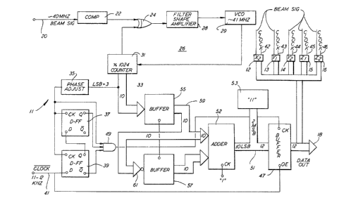
FIG. 1 illustrates a phase counter circuit 11 for one of the
.. . . i. , , . . . " - .
1~7~
g
vibra-ting beams. Identical circuits designated 12-16 are
provided for the ~ther five beams. The outputs of all of these
circuits are coupled onto a data bus 18. With reference to the
phase counter circuit 11, the incoming beam signal which is at
about 40kHz on line 20 is provided as an input to a compara-tor 22
which conver-ts the sine wave signal on line 20 into a square
wave. The square wave is an input to an exclusive OR gate 24
forming part of a conventional phase locked loop 26. In
conventional fashion, the phase locked loop also includes a
filter and shaping amplifier 28, a voltage controlled oscillator
29, having a center frequency of approximately 41MHz and a divide
by 1~24 counter 31 which divides the output of the VCO down to a
frequency equal to the frequency oE the incoming beam signal.
The output of counter 31 is provided on a lO-bit bus 33.
The least significant bit plus 3 from the lO-bit bus 33 is
provided to a phase adjust circuit 35 which may be an adjustable
pulse delay circuit of conventional design which permits
trimming. This signal at about 2.5 MHz is the clock input to a
D-type flip-flop 37 and to a D-type flip-flop 39. The D inpu-t oE
flip-flop 39 is ob-tained from a clock signal on line 41. The
manner in which the clock signal is obtained will be described
below. However, in general, the clock signal on llne 41 and
similar signals (on lines 42-46 of ~'IG. 2) for the other beams
occur in sequence to couple one signal a-t a time onto bus 18.
Thus, the clock signal is also coupled as an output and enable
signal to a buffer 47 coupled to -the output data bus 18. As a
result, data from the bufer 47 is coupled onto the output bus
during the time when the clock signal for that particular beam is
present. The Q output of flip-flop 39 is coupled as the D input
to flip-flop 37. The Q output of flip-flop 37, the Q output of
flip-flop 39 and the output of phase adjust circuit 35 are inputs
to AND gate 49. The output of AND gate 49 is the clock inpu-t to
buffer 47 and will cause to be loaded into the buffer what i5
7~
-- 10 --
present on its input data bus 51. The purpose of the flip~flops
37, 39 and A~D gate 49 are to synchronize the clock signal on
line 41 and the output of the counter 31.
The clock signal on line 41 is normally high. When -the clock
signal goes low, this low signal or logic "0" is transferred to
the Q output on the next output from the phase adjust ci.rcuit 35.
Prior to the occurrence of the pulse out of phase adjust circuit
35, the Q output of flip-flop 39 was high and present at the D
input of flip-flop 37. Thus, on the clock pulse, the Q output of
flip-flop 37 becomes or remains a logic "1", the Q output of
flip-flop 39 becomes a logic "1." Since the
output of the phase adjust circuit 35 is still present, there are
three "1" inputs -to A~ gate 49 and it will owtput a pulse to
clock the data into the buffer 47.
The data into bufEer 47 comprises the output of an adder 52 which
provides the ten least significant bits. The two most
significant bits provided to bufer 47 are from a constant source
53. Although this is indicated as a separate block, -this may be
accomplished simply by tying the two lines to the logic supply.
The adder 52 has as inputs the outputs of bufEers 55 and 57.
Buffer 55 obtains its input from bus 33 from counter 31. The
output of bu~fer 55 is a bus 59 which, after being inverted
through an inverter 61, is the input to buf~er 57. ~uffers 55
and 57 also have their clock lines coupled to the output of gate
49. Thus, on each clock pulse out of gate 49 the value then in
the counter 31 is loaded into buffer 55. The inverted value of
the previous count is loaded into huffer 57. These two
quan-tities are added at adder 52 and the output appears on bus
51. This result is clocked into the buffer 47. On ~he next
clock pulse on line 41, the output of buffer 47 containing this
in~ormation is provided onto the output bus 18.
The output of the adder 52, because it is the sum of the present
~l~ti;~
count and the previous count inverted, i5 a difference and i5
equal -to -the number of counts he-tween two clock pulses.
By selec-ting the clock on line 41 a-t llkHz to 12kHz, it is
ensured that between clock pulses, there will be somewhere
between 3 and 4 cycles of beam frequency. Since measuring
components will always be between 3 and 4 cycles of beam
frequency in the designated period, it is possible to set the
first two most significant bits equal to "l's" at source 53.
Thus, the output on bus 18 is a signal representative of the
frequency of the beam.
Referring to FIG. 2, which is a block diagram and FIG. 3, which
is a timing diagram, the genera-tion o the clock si~nal on line
41, and on lines 42 to 46, will be seen. A clock operatlng in
the range of 176kHz to 192kHz is divided in a divide by 16
counter 60. Thus, assuming a 192kHz input frequency, the output
on line 61 will be at 96kHz, that on line 63 at 48kHz, that on
line 65 at 24kHz and that on line 67 a-t 12kHz. Lines 63, 65 and
67 are inputs to a multiplexer 69 and can selec-t one ou-t of eight
outputs which, when selected will become a logical "0". Thus,
the outputs indicated as MUXl-6 on the timing diagram are
provided as outputs. These then are the clock signals on lines
41-~6 which sequentially cause the outputs of the as~ociated
buffers to be put on the data bus 18.
The data bus 18 is coupled as the two inputs to a 12-bit
multiplier 71 and thus, the output of this multiplier will be the
selected input frequency squared. On the first input cycle, it
will be the frequency of the first beam for the first axis
squared. This output is provided to a 32-bit adder 73 which
receives a second, inverted input rom bus 75. The output of the
adder 73, is thus the difference between its inputs. The output
of adder 73 is provided to a bus 77. It is coupled as an input
. ... ~ . ;~ ;. .
to three 32-bit buffers 79, 81 and 83, one for each of the
sixteen most significant bits of three axes. The output, from
these buffers are provided to a bus 85 which is the input to a
16-bit buffer 87, the output of which is coupled to the
navigation computer 89 with which the accelerometers are
associated.
The outputs of the multiplexer 69 are also provided as inputs to
AND gates 91, 92 and 93. The first two outputs are outputs to
AND gate 91, the second two outputs are inputs to AND gate 92,
and last two outputs inputs to AND gate 93. The result of this
ANDing operation, is that the AND gates are normally high and
go low during the two cycles associated with the one axis. The
outputs of A~D gates 91, 92 and 93 are inputs to OR gates 95, 96
and 97, respectively, these gates having as their second input
the output on line 61, i.e., the output at 96kHz inverted through
an inverter 99. As illustrated on the timing diagram, this
results in two pulses during the enablement period of each of the
three axes. These are provided as clock pulses to the buEfers
79-83.
Also provided is a compa~ator 101 which has as inputs the
outputs of the divide by 16 counter 60. The other side
of the comparator 101 has an input from -the navigation computer
89 and for -the two least significant bi-ts a constant "1" and "0".
The navigation computer 89 when it desires an output for one o~
the axes places on the other two bits an address corresponding to
the desired axes~ The output of -the comparator 101 c]ocks flip-
flops 103 and 106, the outputs of which are ANDed in gate 107,
the output of which is ANDed with the clock signal in gate 109 to
synchronize an input from the computer which is obtained by
ANDing an enable signal and a query signal in AND gate 111. The
operation of this synchroni.zer is exactly like the operation of
the synchroni~.er made up of fllp-flops 37 and 39, and gate 49
.. . . . r ~ :(
~27~
- 13 -
discussed above. The Q output o flip-flop 1~3 also Eorms an
acknowledge signal on line 113 which is Eed back to the computer.
The Q output of flip-flop 103 on line 115 is the output control
input -to the buffer 87. The output of ~ND gate 109 is the clock
input to the bufer 87. The outputs of AND gates 91, 92 and 93
are the output controls for buffers 83, 81 and 79,respec-tively.
Thus, during the first two outputs from multiplexer 69,
corresponcling to the selection of the two beams for the first
axis, the output o buffer 83 is enabled. Similarly in sequence,
buffers 81 and 79 are enablea. By properly addressing and
throu~h the comparator 101, the navigation computer can then
select to have clocked into the output buffer 87 the output of
one of the buffers 79 to 830 The buffer 87 is then controlled
such that its output is provided to the computer.
The data stored in the buffers 79 to 83 corresponds to the
quantity fl2-f22. The first time data is input from the first
beam of the first axis, when there is nothing to subtract from
it, this value is transferred to its associated buffer 83, on the
first of the pair of clock pulses from this OR gate 95. Now the
second beam for tha-t same axis is selected, and its frequenc~ is
squared in the mul-tiplier 71. ~ow, since -the output of the
buffer 83 is enabled, the pre~ious value of fl2 is fed back and
the output of the adder 73 is the difference between f12 and f22.
I~is difference then i~ loaded back into -the buffer 83. The same
thing happens for the other two axes, and these results are
stored in buffers 81 and 79.
The next time it is time to do computations for the first axis,
once again the value fl is squared and subtracted from i-t is the
value stored in the buffer. This value then is f122 - (f212-
fll2) where the second subscript designates the sample number.
The next time, the value f22 is squared and subtracted from it is
, . , , ,, ~
~7~
- 14 -
the value in -the buffer. Thls gives (f222-fl22-~f212-fll2).
The result is f22 minus fl2 plus f21 minus fll. Thus, the
in-tegrating operation is performed in the apparatus.
Although basically, the relationship between beam frequency and
acceleration i5 a second orde.r function, there may be higher
order terms. Such terms can be processed adding additional
stages of multiplication and addition as necessary. Furthermore,
any scaling and bias computations (i.e., referring to equation 7
above, in which the quantity B is a scale factor and the quantity
A is a bias) will involve known quantities which can be
compensated in the navigation computer.
The purpose of the circuitry in FIGS. 1 and 2 is to allow the VBA
to be linearized at a rate sufficientl~ high as to render it
immune from vibration biases produced by intermodulation
distortion. The circuitry meets this requirement in that it is
inherently linear. It achieves this linearity at the expense of
a cyclical resolution error resulting from the squaring process.
For a precisely known reference clock frequency, the roundoff
error should be predictable and will be a repeating ~ycle. Both
the vibration and electronic noise in -the individual beam signals
are expected to be larger than the individual bit resolution of
the phase locked loop. This noise will have the ef~ect of
averaging the resolution error. The RMS error might be expec-ted
to be reduced in proportion to the number of bits over which
vibration and electronic noise affects the operation of the phase
locked loop.