Note: Descriptions are shown in the official language in which they were submitted.
:~3
PHF 86 540 1 7-4-1987
Clock recovery arran~ement suitable more specifi.cally
for an information transmission system usinq the TDMA
principle in one transmission direction.
The present invention relates to a clock
recovery arrangement suitable more specifically for an
information transmission system using the time-division
multiple-access (TDMA) principle in one transmission
direction, the system being comprised of a central station
and remote stations, each station havinq at least one
transmitter circuit and one receiver circuit, information
sent by the transmitter circuit of the central station
to the receiver circuit of the remote stations being
time-division multiplexed and synchroniæed by means of
a phase-locked loop producing at least a multiplex clock
signal, whilst information sent by the transmitter cir-
cuits of the remote stations is transmi.tted to the re-
ceiver circuit of the central station in accordance with
said TDMA principle and is synchronized by the clock
recovery arrangement which includes at least a phase
comparator, a programmable frequency divider, an oscilla-
tor applying a reference signal to the programmable fre-
quency divider.
Such clock recovery arranqements are well-
known, particularly the arrangement described in United
States Patent No. 3,983,498. In said Patent the clock
recovery arranqement uses the output signal of a non-
controlled oscillator by way of reference signal/ this
output signal is divided by means of a programmable
divider and thereafter compared by means of a phase
comparator to the signal conveying the binary information
components at a rate of 24 kbit/s, the output of the
phase comparator being fedback to a control input of
the programmable divider for modifyinq the division
thereof and thus leads to synchronization of the input
information components.
A first disadvantage of such an arrangement
- --
~;:~L~73
20104-82~6
using a non-controll~d osclllator is that at its output a residual
jitter remains which is impermissible for handling e~fectively and
with precision the information components, the more so when the
transmission rate amounts to some Mbit/s.
A second disadvantage of such an arrangement is that the
phase comparator whose output is not "æmoothed" results in too
coarse a quantization of the programma~le di~7ider to obtain a fast
and accurate synchronization.
The present invention has for its object to provide an
arrangement of the type defined above which does not have the
disadvantages of the prior art arrangement.
To that end, the present invention prov~des a clock
recovery arrangement suitable for an information transmission
system using the time-division multiple-access ~TDMA) principle in
one transmission direction, the system including a central station
and remote stations, each station having at least one transmitter
circuit and one receiver circuit, information sent by the
transmitter circuit of the central station to the receiver
circuits of the remote stations being time-division multiplexed
and synchronised by means of a phase-locked loop disposed within
the central station7 said phase-locked loop producing at least a
multiplex clock signal, whilst information sent by the transmitter
clrcuits of the remote stations is transmitted to the receiver
circuit of the central station in accordance with said TDM~
principle and is synchronised upon reception, at the central
station, by the clock recovery arranyement which comprisess a dual
~,
, ,. . .; :,
. ...
73
2010~-8286
loop for fas~ phase reset, the dual loop comprising: a. a first
loop, distinct from said phase-locked loop, which includes an
oscillator, which is locked onto said multiplex clock signal and
which supplies a reference siynal; and b. a second loop, distinct
from said phase-locXed loop, which includes; 1. a phase
comparator; ii. a programmable frequency divider coupled ~o
receive said reference signal; and iii. a sequential digital
filter coupled between said phase comparator and said programmable
frequency divider to averaqe input information to said
programmable frequency divider.
The object of the invention is to provide an effectlve
and fast clock recovery as regards the number of octets assigned
to the synchronization phases. This number of octets must be as
low as possible compared with the total numbar of octets per
frame. Simultaneously, the clock recovery must satisfy precision
and jitter-reduction requirements. The basic idea of the
invention is to use the multiplex clock signal, which is stable
and precise, for an effective frequency setting of the dual phase-
locked loop, this dual loop whose frequency is controlled in this
way then effecting a fast phase reset.
Because the programmable dividar is preceded by a
sequential digital filter used to average tha input information
for said programmable divider, the clock recovery arrangement is
advantageously and rapidly set as to its frequency and is
accurately set as regards its phase.
In addition, in a preferred embodiment of the invention
~:7~3
2010~-8286
the clock recovery arrangement is characterized in that the
frequency of said reference signal produced by said controlled
oscillator is a mul~iple of the frequency of said multiplex clock
signal. The temporal accuracy of the clock recovery is thus
increased slnce locking the dual loop onto the multiplex clock
signal is effected at a high frequency.
The following description given by way o~ example wlth
reference to the accompanying drawings, will make it better
understood how the invention can be put into e~fect.
Fig. 1 shows schematically an information transmission
sys~em utilising the clock recovery arrangement according to the
invention;
Fig. 2 shows a phase-locked loop used in the
transmission direction from the central station to the remote
stations;
Fig. 3 shows a clock recovery arrangement according to
the invention;
Fig. 4a shows a state diagram relating to the phase
comparator used in the second loop and Fig. 4b shows a concise
circuit diagram of said phase comparator;
Fig. Sa shows a state diagram relating to the sequential
digital filter and Fig. 5b shows a concise circuit dlagram of the
sequential digital filter.
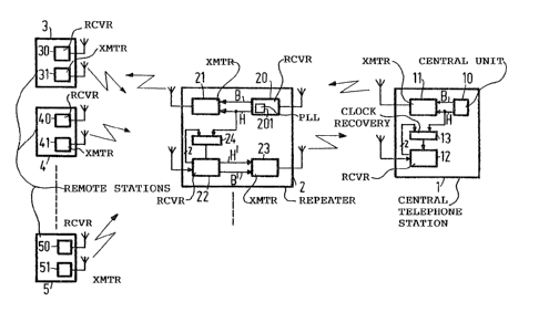
Fig. 1 shows schematically an information transmission
system in which the clock recovery arrangement according to the
invention is used. The system shown is a radio relay system of
~..2~3
20104-8286
the point-to-multlpoint type ~enerally used in rural telephone
equipment. A single central station 1 communicates with n remote
stations, for example the repeater station 2 and the end stations
3, 4, 5, ... . Depending on the configuration of the system as
regards the number of subscribers and the area to be served, ~here
may be one or a plurality of repeater stations or even no repeater
station at all.
3b
. -
73
PHF ~6 540 -4- 7-4-1987
The information components conveyed by the
central unit 10 of the central station 1 are applied in
the form of binary siqnal B plus clock siqnal H to the
modulator of the transmitter circuit 11, the binary
signal B is transmitted to the receiver circuit 20 (or
to the plurality of receiver circuits when there is more
than one repeater station) of the repeater station 2,
the binary signal B and the clock signal H recovered
by means of a phase-locked loop 201 are transmitted to
the transmitter circuit 21 which transmits the binary
information components to the various receiver circuits
30, 40, 50, ... of the end stations 3, 4, 5, ... .
Thus the central station 1 transmits the
information omnidirectionally and simultaneously to the
lS set of n remote stations which select the information
components intended for them, this is the transmission
direction which will be denoted as the multiplex direc-
tion.
Inversely, because the remote stations cannot
all transmit simultaneously, they have a special time
interval assiqned to them during which they can transmit
their information to the central station, this technique
being known as time-division multiple-access (TDMA) and
so this transmission direction will be denoted the TDMA
direction.
The information sent by each remote station is
partitioned in what are commonly called packets .
The number of packets is linked with the
number of telephone channels the system can handle.
In addition to the telephone channels a predetermined
number of packets are provided for manaainq the system.
For example, two packets can be associated~ for the
purpose of management, with 30 packets used for te]ephone
channel transmission, resulting in a total of 32 packets.
For each packet, the number of octets relating to the
information to be transmitted is chosen such that the
real transmission period is sufficiently lonq with respect
to the time needed for putting the transmitter and
~L2~L~
PHF 86 540 -5- 7-4-1986
receiver circuits in operation, but sufficiently short
with respec~ to the time needed for arranging the in-
formation into packet,s to avoid disturbing echoes during
a telephone conversation. Thus, a lenqth of 64 octets
of pure information corresponds to a packet transmission
period of, for example, 8 ms. Service octets (for example
8) are added to these information octets to improve the
efficiency of the transmission, which entails anincrease
in transmission rate. A predetermined number of service
octets are reserved for the actual clock recovery.
The different packets are transmitted by the
transmitter circuits 31, 41, 51, ..., of the end stations
3, 4, 5, ..., to the receiver circuit 22 (or a plurality
of receiver circuits when there is more than one repeater
station) of the repeater station 2, thereafter the trans-
mitter circuit 23 of the repeater station 2 transmits
the packets to the receiver circuit 12 of the central
station 1.
In accordance with the invention, there is
provided a clock recovery arrangement (13, 24) whichis
more specifically suitable for an information transmission
system using the ~: time-division multiple-access (TDMA)
principle in one transmission direction, the system beinq
comprised of a central station(l) and remote stations
(2, 3, 4, 5, ...) each station havinq at least one
transmitter circuit (11, 21, 23, 31, 41, 51, ...) and a
receiver circuit (12, 20, 22, 30, 40, 50, ...), the
information components trancmittea by the receiver circuit
(11) of the central station (1) to the receiver circuits
30 (20, 30, 40, 50, .. ) of the remote stations (2, 3, 4,
5, ...) being time-division multiplexed and synchronized
by means of a phase-locked loop (201, described with
reference to Fig. 2) prod~cing inter alia a multiplex
clock signal (H), whi]st the information components
35 transmitted by the transmitter circuits (23, 31, 41,
51, ...) of the remote stations (2, 3, 4, 5, ...) are
transmitted to the receiver circuit (12) of the central
station (1) in accordance with the TDMA principle and are
~73
PHF 86 540 -6- 7-4-1987
synchroni7.ed by the clock recovery arrar.gement (13,
24) which comprises at least a phase comparator, a
programmable frequency divider and an oscillator applyinq
a reference signal to the proqrammahle frequency divider,
5 said clock recovery arranqement (13, 24) being charac-
terized in that it is constituted by a dual loop (des-
cribed with reference to Fig. 3) for a fast phase reset,
the first loop including the oscillator which is locked
onto the multiplex clock signal H and itself applies
the reference signal to the second loop including inter
alia the phase comparator and the programmable frequency
divider.
Thus, during the packet transmission, the in-
formation components are applied to the modulator of the
15 transmitter circuit (23, 31, 41, 51, ... ) in the form of
a binary signal plus a clock signal (B~H), the clock
(H) only heing provide~ for fixing the sampling instants.
During the receiving phase of the stations
(1, 2, ...) the information components must be applied
to the output of the demodulator of the receiver circuit
(12, 22, ...) in the same format of binary signal B'
plus clock H'. Since only the binary signal B' is
transmitted via radio, the clock ~' must be recovered
from the transitions in the demodulated binary ~iqnal,
i.e. a clock recovery operation has to be performed.
So as to ensure that this operation is effected
correctly, it cannot be performed on the binary infor-
mation signal corresponding to the speech signal because
there is only a very small probability that a transition
3D is obtained at each transmitted bit, the sequences of 1
or O being rather frequent in a speech signal. To that
end, clock octets are sent at each start of the trans-
mission of a packet, thus producing a transition at each
transmitted bit, the clock recovery phase being of
necessity achieved at the end of the reception of these
octets.
In the information transmission system used,
a four state modulation (4-QAM = 4-state Quadrature
~:7L~3
PHF 86 540 -7- 7-4-1987
Amplitude Modulation~ a non-limitative choice for employ-
ing the invention) has been opted for, thus two half-
rate hinary frames are received and only half the number
of the transmitted transitions is received but that num-
ber is received twice.
Thus, in the TDMA transmission direction,for example five octets are reserved for the clock re-
coveryS that is to say 40 bits or 2 x 20 transitions
at the output of the receiver circuit.For the case of
a clock recovery by means of a phase-locked loop, thinking
that it is possible to obtain a correct frequency stability
simultaneously with a very fast phase recovery, is wish-
ful thinking and this consideration has lead Applicants
to an advantaqeous separation of these two functions.
The multiplex clock signal H recovered by means of the
phase-locked loop 201 in the repeater station 2 is used
by the clock recovery arrangement 24 for an effective
frequency settinq, this ~iqnal H being applied to one
input of the arranqement 24, whose second input receives
the hinary signal ~2 binary data streams) after demodulation
by the demodulator of the receiver circuit 22, the ar-
rangement 24 whose frequency is controlled thus then
effecting a fast phase reset. The same holds for the
central station 1 when there is a plurality of repeater
stations 2, which is generally the case; the clock
signal H is transmitted, by the loqic arrangement asso-
ciated with the central unit 10, directly to an input
of the clock recovery arrangement 13 for an effective
frequency setting, whilst the binary signal (2 binary
data streams) after demodulation by the demodulator
of the receiver circuit 12 is applied to a second input
of the arrangement 13, the arrangement 13 then effecting
a fast phase reset.
Fig. 2 illustrates a phase-locked loop used
in the transmission direction from the central station
to the remote stations, that is to say in the mu]tiplex
direction. The phase-locked loop 201 (Fig. 1) will now
be described brief]y with reference to Fig. 2, which loop
~2~73
PHF 86 540 -8- 7-4-1987
is provided, moreover, in each one of the receiver
circuits (20, 30, 40, 50, ...) of the remote stations
(2, 3, 4, 5, ...) for Glock recovery in t.he multiplex
direction.
s The problems as re~ards the clock recovery
occur for both the TDMA direction and the multiplex
direction. However, in the latter case there is only
one transmitting station and the synchronization is al-
ways effected on the same phase, in contradistinction
to the TDMA direction for which synchronization must
be effected at the start of each packet. The problems
existing in the fast phase recovery are then absent,
for the multiplex direction which renders it possible to
realize a phase-locked loop with sufficient inertia to
ensure an appropriate frequency stabi.lity, which fre-
quency stability will be uti].ized in the TDMA direction,
since each TDMA receiver circuit. (12j 22, Fi.q. 1) is
associated with a multiplex transmitter circuit (11,
21, Fig. 1) whose multiplex clock siqnal H is either the
signal produced by the logic arrangement associated
with the central unit 10 of the central stationl, or the
recovered signal present at the output of the phase-
locked loop 201 of a receiver circuit of a repeater
station 2.
The demodulator of the receiver circuit 20
applies to the input of the phase-locked loop 201 two
binary data streams AM and BM (resultinq from the 4-
p~ase modulation) of frequency H/4. The input of the
phase-locked loop 201 is formed by a differentiatinq
circuit 2010 performin~ the operation ¦d/dt¦ (the ab-
solute value of d/dt), which circuit has for its object
to recover the clock information components contained
in the two binary data streams AM and BM by revealinq the
totality of the transitions.
The output of the circuit 2010 applies the clock
information components at the ra.te H/2 to an input of
a phase comparator 2011 whose outPut is connected to
the input of a sample-and-hold circuit 2012. A second
PHF 86 540 -9- 7-4-1987
output of the cireuit 2010 controls opening of the sample-
and-hold cireuit 2012 with the aid of a eontrol signal
AT generated when an absenee of a transition is deteeted,
the sample-and-hold circuit 2012 actually servinq to
store the loop voltage in the absence of a transition.
The output of the eireuit 2012 is eonneeted to the input
of a voltage-eontrolled oscillator 2013 whose output signal
has a frequeney of ~H. In order to reeover the cloek
signal H~ the output signal of the oscillator 2013
is divided by 8 by means of a frequency divider eireuit
2014 at whose output said e]oek signal H beeomes avail-
able. This output signal is also eonveyed to the phase
eomparator 2011; actually the clock signal is first
divided by 2 by means of a frequeney divider eireuit 2015
and this signal of frequeney H/2 is applied to a seeond
input of the phase eomparator 2011 to be eompared to the
signal of frequeney H/2 present at the first input of
the phase eomparator. The parameters of the phase loeked-
loop 201 thus realized are optimized in sueh a manner
as to provide the best possible eompromise between the
frequeney stability and the aequisition time neees~ary
to obtain ~his stability.
Fig. 3 shows a eloek recovery arranqement
aceording to the invention, whieh arrangement is used
in the TDMA transmission direetion and, in Fiq. 1, is
referenced by 24 when it is provided ina repeater station
2 and referenced 13 when it is ineluded in the eentral
station 1, the TDMA elock recovery problem only existing
in a repeater station or a eentral station. In Fig. 3
the cloek recovery arrangement 24 is shown as being
eonstituted by two loops, the first loop 24A is very
similar to the phase-locked loop 201 described with re-
ference to Fig. 2, the main differenee being that it has
neither a differentiating circuit nor a sample-and-hold
circuit. In this ease these eireuits are superfluous,
as this first loop is, in aeeordance with the basic idea
of the invention, advantaqeously synchroni~.ed with the
multiplex cloek signal H and eonsequently all the clock
. . . . .
PHF 86 540 -10- 7-4-1987
transition~ are always present. Thus, in a repeater
station 2 the signal H at the input of the arrangement
24 is the clock signal recovered at the output of the
phase-locked loop 201 (in the central station 1 the siqnal
at the input of the arran~ement 13 is the clock signal
H sent directly by the logic arrangement associated with
the central unit). The clock signal H is thus applied
to the input of this first loop 24A where it is divided
by 2 by means of a frequency divider circuit 241. The
output of the circuit 241 is connected to an output of a
phase compar2tor 242 which thus receives the siqnal
of frequency H/2. The output of the phase comparator
242 is connected to the input of a voltage-controlled
oscillator 243 at whose output the signal has a frequency
8H. Thereafter the output si~nal of the oscillator 243
is divided by 16 by means of a frequency divider circuit
244 whose output is fedback to a second input of the
phase comparator 242 for comparing this signal of fre-
quency H/2 to the siqnal of frequency H/2 present at the
first input of the comparator 242. Thus an optimum
frequency setting is realized. The signal used by the
second loop 24B for a fast phase recovery is the output
signal of the oscillator 243 which has been processed in
the firct loop 24A and whose frequency has been set with
precision. This signal of a frequency RH is multiplied
by 2 tto obtain 16 H) with the aid of a frequency multi-
plier circuit 245, which enables a correction accurate
to 1/32 bit (defined with respect to H/2). Because the
precision required for the system operating in accor-
dance with the TDMA principle in order to control thedelays of the stations is an accuracy to 1/8 bit (with
respect to H/2), it should be noted that advantaqeously
the precision as regards the phase control is four times
better. The clock recoveryin the TDMA direction is there-
fore reduced to a fast phase reset of the local signalon the data received. The demodulator of the receiver
circuit 22 applies two binary data streams AA and BA
(resulting from the 4-phase modulation) of frequency H/4
~, :
PHF 86 540 -11- 7-4-1987
to the input of the second loop 24B, The input of the
second loop is constituted by a differentiating circuit
246 for performing the operation ¦d/dt~ (absolute value
of d/dt), which circui.t has for its function to recover
the clock information components contained in the two
binary data streams AA and BA by revealing the transitions
of the signal present at this input. The clock information
components outputte~ by the circuit 246 are applied at
the rate H/2 to a first input of a phase comparator 247
to whose second input a siqnal of frequency H/2 is
applied which is compared to the signal present at the
first input of the circuit 247. This comparison signal
applied to the second input of said ci.rcuit 247 is
supplied by a programmable frequency divider 248 which
15 effects a divi.sion by 30, 31, 32, 33 or 34. The program-
mable frequency divider receives at one of its inputs the
reference signal set to the frequency 16H and present
at the output of the multiplier circuit 245 of the first
loop thereby ensuring the link between the first and
second loops. The signal of frequency 16H is also supplied
to the phase comparator 247 for use as a sequencing clock.
The progrmmable divider 248 divides the signal of
frequency 16H by 32 when the phases of the signal of
frequency H/2 at the input of the phase comparator are
identical, and by 30 or 31 when the signal of frequency
16H after division has a phase lag relative to the phase
of the TDMA signal present at the output of the circuit
246 so as to offset the phase lead of the TDMA signal, and
finally by 33 or 34 when the signal of the frequency 16H
after division has a phase lead relative to the phase of
the TDMA si.gnal present at the OlltpUt of the circui.t 246
and so as to offset the phase lag of the TDMA signal.
Thus the phase is always corrected with respect to the
TDMA signal in accordance with a procedure which will be
described hereinafter with reference to Fig. 4a and in
accordance with the output information of the phase com-
parator 247 which indicates leading, lagqing or equality
of the phase. It will be clear that the clock recovery
PHF 86 540 -12- 7-4-1987
arrangement 13 of the centra]. station 1 is in its
totality identical to the arrangement 24 described i.n
the fore~oing.
In accordance with a further aspect of the
invention, the clock recover~ arrangement whose second
loop inc].udes inter alia a pro~rammable frequency divider
is further characterized in that saia proqrammahle divider
is preceded by a sequential di~ita]. filter. Actually,
the information as regards the lag, lead or equality of
tO the phase applied by the phase comparator 247 to the
programmable divider 248 is too coarse for direct usage
as a control information for the division factor, and for
that reason these inform~tion components are averaged
by means of a sequential digital fi].ter 249 which inter-
prets said iriformation components received from the
phase comparator in accordance with a procedure des-
crihed hereinafter (Fig. 5b). The sequential diqital
filter also receives the signal of the frequency 16H
which acts as a sequencing clock.
The output of the phase comparator 247 is
connected to the input of the sequential diqital filter
249 which at its output sllpplies a control signal for
the division factors which signal is applied to an input
of the programmable divider 248. The programmakle divider
248 thus fedback then produces at its output which is
connected to an input of the recei.ver circuit 22 the
clock signal H' of the TDMA clock necessary for reading
the packets cominq from the same remote station, is then
re-adjusted in accordance with the same procedure for
reading the packets transmitted by another remote station
etc. The clock signal H' is identical to the clock signal
H as regards its frequency~ but has a phase that is
locked onto the input data slgnal.
The divider 248 programmable for a divide-by-
35 30, -31,-32,-33 or -34 operation is, for example, con-
stituted by an 8-hit counter that is assemhled ~rom two
4-bit counters arranged in cascade, fedback to the res-
pective deci~al positions 226, 225, 224, 223, 222 in
,
~3
PHF 86 540 -13- 7-4-1987
accordance with the followin~ Table:
Counter Bit 8 Bit7 Bit6 Bit5 Bit4 Bit3 Bit2 Bitl
va]ue (128) (64) (32) (16)(8) (4) (2) (1)
222 1 1 0 1 1 1 1 0
5 223 1 1 0
224 1 1 1 0 0 0 0 0
225 1 1 1 0 0 0 0
226 1 1 1 0 0 0 1 0
227 1 1 1 0 0 0
10228 1 1 1 0 0 1 0 0
229 1 1 1 0 0 1 0
230 1 1 1 0 0 1 1 0
231 1 1 1 0 0
232 1 1 1 0 1 0 0 0
15233 1 1 1 0 1 0 0
234 1 1 1 0 1 0 1 0
235 1 1 1 0 1 0
236 1 1 1 0 1 1 0 0
237 1 1 1 0 1 1 0
20238 1 1 1 0 1 1 1 0
239 1 1 1 0
240 1 1 1 1 0 0 0 0
241 1 1 1 1 0 0 0
242 1 1 1 1 0 0 1 0
25243 1 1 1 1 0 0
244 1 1 1 1 0 1 0 0
245 1 1 1 1 0 1 0
246 1 1 1 1 0 1 1 0
247 1 1 1 1 0
30248 1 1 1 1 1 0 0 0
249 1 1 1 1 1 0 0
250 1 1 1 1 1 0 1 0
251 1 1 1 1 1 0
252 1 1 1 1 1 1 0 0
35253 1 1 1 1 1 1 0
254 1 1 1 1 1 1 1 0
255
~3
PHF 86 540 -14- 7-4 1987
In these circumstances, in accordance with the
preceding Table, the following statements hO] d when the
(decimal) counter value !or counter position) at the
preset instant is 255:
- a division by 30 corresponds to the counter
value of ~26;
- a division by 31 corresponds to the counter
value of 225;
- a division by 32 corresponds to the counter
value of 224;
- a division by 33 corresponds to the counter
value of 223;
- a division by 34 corresponds to the counter
value of 222.
When studying the preceding Table for the
counter values 222, 223, 224, 225, 226, it will be noted
that the bits 7 and 8 are always in the 1 state, con-
sequently a high level is continuously applied to these
two, interconnected, inputs. It will also be noted
that the bits 5 and 6 are a]ways complementary and that
bit 5 is always in the same state as the bits 3 and 4,
consequently the inputs correspondin~ to the bits 3, 4,
5 are mutually interconnected and the input correspon-
ding to bit 5 is also connected to the corresponding
input of bit 6 via an inverter ci.rcuit. The inputs
corresponding to the bits 1, 2 and 3 are each connected
to a division factor control output of the sequential
digital filter 249. Thus, when there is applied to the
respective inputs corresponding to the bits 1, 2 and 3:
- the binary value 011, the correspondinq
division factor is 34;
- the binary value 111, the corresponding
division factor is 33;
- the binary value OOO, the correspondinq
division factor is 32;
- the bi.nary value 100, the corresponding
division factor is 31;
- the binary value 010, the corresponding
PHF 86 540 -15- 7-4-1987
division factor is 30.
As the clock input signal of the programmab]e
divider 248 thus obtained is the signal having a fre-
quency of 16H present at the output of the multiplier
circuit, 245 then the signal of the frequency H trans-
mitted towards the receiving circuit 22 (Fig. 1) is
present at the output of rank 4 (bit 4) and the phase
resetting clock signal H/2 applied to the second input
of the phase comparator 247 is present at the output of
rank 5 (bit 5).
Fig. 4a is a state diagram relating to the
phase comparator employed in the second loop 24B, Fig. 4b
shows a concise circuit diagram of this phase comparator
247. The comparator 247 is a digital phase comparator
which is actually constituted by a sequential automatic
device. The sequencing clock is the siqnal of the fre-
quency of 16H and the impu]ses applied to the inputs of
the automatic device oriqinate on the one hand from the
detection of the transitions in the,received data signals
performed by the differentiatinq circuit 246 and on the
other hand fro~l the phase resetting clock signalat the
output of rank 5 of the programmable divider 248.
The outputs convey the pulses relating to one
of the three possible situations: phase lead, phase laq
or phase equality in accordance with the sequence read
at the inputs and in conformity with the state diaqram
described below.
For a proper understanding of the following
description the impulse signal corresponding to the re-
ceived data and outputted by the differentiating circuit
246 is denoted Hl or Hl (depending on whether it is in
the high or the ]ow state, respectively) and its duration
is equal to one period of the sequencinq clock; the
phase reset,ting clock siqnal outputted by the divider
35 248 is denoted H2 or H2 (dependinq on whether it is in
the high or low state, respectively). The signals Hl,
Hl, H2 and H2 are input variables.
In the diagram of Fig. 4a, six states can be
~r~3
PHF 86 540 -16- 7-4-1987
defined by means of, for example, three D-type flip-flops
(FFl, FF2, FF3) which are clocked at the rate of the
signal of frequency 16H. The state F,O is the initial state
(at the instant of circui.t activation or the instant
of cycle return) and if the available information is Hl,
H2, the subsequent state is the state El decoded by means
of a decoding logic (block Ll) constituted, for example,
by an array of logic circuits to whose inputs the input
variables and the output states of the 3 D~flip-flops
are transferred. The output states of the D-flip- flops
are also tra~.sferred via the logic block I.l to a register
RE which conveys the useful information to the sequential
digital filter, information such as phase delay DE~ phase
lead A, phase equality P, positioning C, reset-to-zero RC
of a pu].se counter provided at an input of the sequential
digital filter and T which indicates the absence of the
signal H].. When the circuit is activated or at the start
of a cycle, the flip-flops are reset to zero (si~nal R,
which is a sync pulse).
Thus, when at the state Eo the information
HlH2 has been decoded, the reset-to-zero RC of the
output register of the phase comparator is set to its high
state during a period of the sequencing clock to effect
a reset-to-zero of the pulse counter at the i.nput of the
sequential digital filter. As the information HlH2 in-
dicates that the clock Hl of the received data leads the
clock si.gnal H2, the output C of the register RE of the
comparator is set to a state such that the pulse counter
can count the periods of the sequenci.ng clock (16 H) until
the clock H2 itself rises: this is the transi.tion to the
state E2 durinq which a setting takes place for the
output LEAD (output A) connected to a counter in the
sequential digital fil.ter for counting the information
of the type LEAD When the signal H2 goes down while
the signal Hl i.~ in the low state the phase compar~ox
returns to the state EO.
However, when the siqnal H2 changes to the low
state while the signal Hl is still in the hiqh state, a
` ~27~573
PHF ~6 540 -17- 7-4-1987
double transition is detected, which then causes the
pulse counter to be reset to zero and a return to the
state El occurs, followed by a transition to the state
E2 when the clock H2 passes to the high state again,
the cycle then becoming identical to the previously
described cycle when the clock Hl changes to the low
state before the clock signal H2.
The same procedure is followed when the in-
formation HlH2 reappears.
When in the state EO the information H2Hl is
decoded, simultaneously the reset-to-zero RC of the output
register RE of the phase comparator set to its high
state to effect a reset-to-zero of the pulse counter
at the input of the sequential digital filter. The output
C of the register RE of the phase comparator is set to
provide that the impulse counter counts at the rate of the
signal of frequency 16H, this is the transition to the
state E3; if the clock signal H2 qoes down before the
clock signal Hl rises, the counter stops counting and an
absence of a transition in H](T) is detected, which
information is transferred to the pulse counter of the
sequential digital filter and a return to the state EO
occurs. If in contrast therewith the clock siqnal Hl
rises before the clock siqnal H2 goes down, the input
information H2Hl then indicates that the clock signal
Hl lags the clock signal H2 and the pulse counter
controlled by the output C of the register RE stops
counting at the instant at which said clock signal Hl
rises, this is the transition to state E4 during which
a setting takes place for the output LAG (output DE)
connected to a counter in the sequential digital filter
for counting the information of the type LAG. When the
signal Hl goes down the phase comparator returns to the
state EO. The same cycle is repeated when the information
H2Hl reappears.
Finally, when in the state EO the information
HlH2 is decoded, simultaneously the reset-to-zero RC
of the output register RE of the phase comparator is
~2'7~L~73
PHF 86 540 -18- 7-4-1987
set to its high state to effect the reset-to-zero of the
impulse counter at the input of the sequential diqital
filter. In that case the input information indicates
that the clock signals H1 and H2 change simultaneously
to the high state and are in-phase, this is the tran-
sition to the state E5 durinq which a setting takes
place for the output PHASE-EQUALITY (output P), thic
output is connected to a counter in the sequential diqital
filter for c~unting the information of the type PHASE-
EQUALITY. When the clock signals Hl and H2 go do~n thephase comparator returns to the state EO. This cycle is
repeated until the information HlH2 reappears.
In this way the digital phase comparator pre-
cedes the sequential digital filter and applies thereto
the information of the type LEAD, LAG, PHASE-EQUALITY.
It renders it also possible to effect the reset-to-zero
operations of the pulse counters of the sequential
digital filter. It also transfers a countinq information
to the pulse counters, it thus being possible to deter-
mine the shift ketween the risinq edges of the two clocksignals H1 and H2, which information is used to define
whether a division by 30 or by 31 must be effected for
the case in which there is a simultaneous transfer of
information of the LEAD type, or by 33 or 34 for the
case in which there is a simultaneous transfer of infor-
mation of the LAG type. The division by 32 is
effected when information of the type PHASE-EQUALITY is
transferred. Finally, the digital phase comparator ren-
ders it possible, when an absence of a transition is
detected (a chan~e from the state E3 to the state EO),
to readjust the programmable divider to a division by
32, using this information.
Fig. 5a is a state diagram relatinq to the
sequentia] digital filter 2~9 provided advantaqeously
hetween the digital phase comparator 247 and the pro-
grammable divider 248. Fig. 5b is a concise circuit
diagram of the sequential diqital filter. The sequential
digital filter is also constituted by a sequential automatic
~ ~73
PHF 86 540 -19- 7-4-1987
devi~e whose sequencing clock si~nal is also the siqnal
of frequency 16H. The inputs of this automatic device
receive the information outputted directly or inc7~irectly
by the digital phase comparator 247. The information
uced directly are the phase-equality information P and
the absence-of-transition information T, the i.nfor-
mation used indirectly is the information of the type
LEAD ~A), LAG (DE) and the countiny information C. The
last three types of information are used after passage
through respectively a counter C1 counting the infor-
mation of the type LEAD, a counter C2 countinq the in-
formation of the type LAG and a pulse counter C3 which
has already been mentioned in the description with re-
ference to Fiq. 4. Counting the information P of the
phase-equality type H is effected by a counter C4.
The sequential digital filter interprets the
information outputted by the phase comparator in accor-
dance with the following criteria.
When 4 pulses of the LEAD type have been
counted or simultaneously two pulses of the LEAD type
and a deviation exceedinq 8 bits, a command to di.vide
by 30 is given when the deviation detected is qreater
than or equal to 8 bits or a command to divide by 81
when the deviation detected is less than 8 bits, all
thic as long as information of the type L7~AD is received.
As soon as one information of the type I.AG or one in-
formation of the PHASE-EQ~7ALITY type is received the pro-
grammable divider is re-adjusted to the divide-by-32
pOcition .
When 4 pulses of the LAG type have been counted
or simu].taneously 2 pulses of the type LAG and a devi-
ation exceeding 8 bits, a command by divide by 34 is
given when the deviation detected is qreater than or
equal to 8 bits, or a command to divide by 33 when the
deviation detected is less than 8 bits, all this as long
as information of the LAG type is received. As soon as
one information of the LEAD type or one information of
the PHASE-EQUALITY type has been counted the pro~rammable
~2~ 73
PHF 86 540 -20- 7-4-1987
divider is re-adjusted to the divide-by-32 position.
When 6 pulses have been counted and they are
predominantly of the LEAD or LAG type (that is to say
3 pulses of the LEAD type and 3 pulses of the LAG type)
s the sequence is re-initialised and a command to divide
by 32 is qiven.
Finally, when a pulse of the PHASE-EQUALITY
type has been received an order to divide hy 32 is qiven.
After reception of 3 pulses of this type, the counters
counting the information of the type LEAD, LAG or
PHASE-EQUALITY are reset to zero.
Used thus, the sequential digital filter renders
it possible to correct advantageously and rapidly a
significant phase deviation, for example a deviation of
16 bits during the reception of 16 information pulses
of the LEAD or the LAG type, that is to say 32 clock
bits out of the 40 available bits (2x20 transitions),
8 bits or 2 x 4 transitions thus remaininq for completinq,
if necessary, the phase control. This filter simultane-
ously effects an effective filter operation by avera~inqthe output information of the digital phase comparator,
which information is too coarse to be suitable for direct
usage as a division command for the programmable divider.
The state diagram of Fiq. 5a shows three states
E'O, E'l and E'2 correspondinq to the division by 32, by
30 or 31 and ky 33 or 34, respectively~ These three
states are defined by means of, for example, two D-type
flip-flops (FF4, FF5) which are clocked at the rate of
the signal of frequency 16H. This signal having the fre-
quency 16H is used at the same time as the clock signalfor the LEAD counter Cl~ LAG counter C2 and PHASE-
EQVALITY counter C4 and for the pulse counter C3. The
states are decoded by means of a decoding logic (block
L2) constituted by, for example, an array of logic
circuits to whose inputs the output states of the three
LEAD, LAG, and PHASE-E9lJALITY counters and the output
states of the 2 D-flip-flops are applied. The decoding
logic L2 renders it also possible to effect a reset-to-
;7~3
PHF 86 540 -21- 7-4-1987
zero for the three counters LEAD !siqnal RA), LAG
(siqnal RD) and PHASE-EQUALITY (signal RP) and finally
by means of 3 of the outputs of L2 the division commands
Dl, D2, D3 are ~iven to the programmable divider. The
pulse counter C3 renders it possible to determine whether
the phase shift is greater than or equal to 8 bits and
thus supplies a necessary infor~ation to com~and the
division either by 30 if simultaneously the LEAD counter
Cl has counted at least two pulses, or by 34 if simul-
taneously the LAG counter C2 has counted at least twopulses.
When the device is activated, the 2 D-flip-
flops (FF4, FF5) are reset to zero (signal R which is a
sync pulse), the 4 counter Cl, C2, C3, C4 are likewise
reset to zero (siqnals RA, RD, RP with the aid of the
logic L2 and the signal RC). Consequently, the activation
of the device corresponds to a division by 32. Each in-
formation indicating the absence of the transition T
causes a division by 32 without reset-to-zero for the
counters Cl, C2, C4. The division by 32 is represented
by the state E'O, this state E'O is preserved if after
the reception of 6 consecutive pulses 3 pulses have been
counted by the LEAD counter (3A) and 3 pulses by the LAG
counter (3DE) or vice versa. At the end of countinq these
6 pulses a reset-to-zero is effected for the LEAD coun-
ter (RA) and the LAG counter (RD).
When 4 pulses of the LEAD type (4A) are counted
by the LEAD counter Cl or when 2 pulses of the LEAD type
are counted and there exists a deviation exceedinq 8 bits
(2A.~ 8) a transition to the state E'l takes place, that
is to say a chan~e is effected to a division by 30 when
the pulse counter C3 has reqistered a shift greater than
or equal to ~ bits or a command to divide by 31 if the
shift is less than 8 bits. In the state E'l, if the
counter C4 detects PHASE-EQUALITY once (lP), a return
to the E'O state ~division by 32) is effected and at the
same time a reset-to-zero is effected for the LEAD
counter (RA) an~ the LAG counter (RD). If likewise, in
.
73
PHF 86 540 -22- 7-4-1987
the state E'l one information of the LAG type (lD) is
counted by the LAG counter C2, a return to the E'O state
is effected (division by 32) and at the same time a
reset-to-zero is effected for the LAG counter (RA).
Inversely; when 4 pulses of the LAG type (4DE)
are counted by the LAG counter C2 or when 2 pulses of
the LAG type are counted and there exi~ts a deviation
greater than 8 bits (2DE.~ 8) a transition to the state
E'2 takes place, that is to say to the division by 34
when the pulse counter C3 has registered a shift greater
than or equal to 8 bits or to the division by 33 when
the shift is less than 8 bits. In the state E'2, if
PHASE-EQUALITY is detected once (lP) by the counter C4,
a return to the state E'O is effected (division by 32)
and at the same time a reset-to-zero is effected for the
LEAD counter (RA) and the LAG counter (RD). If in this
same state E'2, one information of the LEAD type (lA)
is counted by the LEAD counter Cl, a return to the state
E'O (divisi.on by 32) is effected and at the same time a
reset-to-zero is effected for the LAG counter (RD).
Finally, if in the state E~O (division by 32)
3 consecutive pulses are counted by the PHASE-EQUALITY
counter C4 (3P), this state is of course maintained (and
so the division by 32), but in addition the LEAD, LAG
and PHASE-EQ~ALITY counters are reset to zero by the
respective siqnals RA, RD, RP.
Thus, the sequential digital filter applies,
via its 3 respective outputs Dl, D2, D3, the division
commands to 3 of the inputs of the programmable divider
corresponding to the bits l, 2 and 3 in accordance
with the following codes:
- binary value 011 correspondinq to a divi~ion
by 34;
- binary value lll correspondinq to a division
by 33;
- bi.nary value 000 corresponding to a division
by 32;
- binary value lO0 corresponding to a division
~127~S~3
PHF 86 540 -23- 7-4-1987
by 31;
- binary value 010 corresponding to a division
by 30.
' ~ '
.
: