Note: Descriptions are shown in the official language in which they were submitted.
1;~71~3t)
This invention relates to opto-electronic devices
and, in particular, to optical amplifiers obtained by
coating the facets of a laser with anti-reflection coating.
Semiconductor lasers are well known devices which
5 are used to generate light. Their operation depends upon
the reflection of light generated by the device back into
the device. It is also desired to utilise a "laser" to
amplify a received optical signal. In this application it
is desired that the device shall respond only to the
10 received signal and in order to achieve or get close to
this result it is necessary to eliminate as far as it is
possible the reflection of light back into the device.
For this purpose, anti-reflection coatings are
applied to the facets of the laser and a wide variety of
15 metal oxides have been proposed for these coatings, e.g.
Al23~ Sc203, Zro2 and CeO2. Our co-pending Canadian
Application Serial No. 403, 332 states that oxides of Y,
Gd, Nd and La give particularly good results.
We have realized that some metal oxide coatings
20 fail to display their full potential as anti-reflection
coatings. In addition we have, most surprisingly, found
that the incorporation of a thin interlayer between the
effect coating and the semiconductor device substantially
enhances the performance.
Accordingly, the invention provides an opto-
electronic device which has, on at least one of its facets,
a composite coating effective to reduce the reflectivity of
the said ~acet, wherein said composite coating includes an
effect coating and an interlayer for improving the chemical
30 compatibility between the effect coating and the device,
said interlayer being not more than 30 nm in thickness.
The interlayer should provide a complete cover
between the device and the effect coating but it should be
so thin that, by itself, it would have little or no effect
35 on the optical properties of the coated device. It is
surpri6ing that such thin layers exert a substantial
effect.
C
1 ~ 7~
-- 2 --
Furthermore the material used for the interlayer
may be less effective as an anti-reflection coating than
the material of the effect coating. Therefore it would be
expected that, even if such a thin layer should produce a
noticeable effect, that effect would be detrimental,
whereas it is substantial and bene~icial.
The invention is particularly suitable for use
where the effect coating is composed of oxides of Y, Gd,
Nd or La and the substrate is a laser such as an indium-
gallium arsenide-phosphide laser. In this case we have
found that A1203 is particularly suitable as the
interlayer. The thickness of the interlayer is preferably
10 to 30 nm e.g. 15 to 25 nm in absolute terms. In
relative terms the interlayer is 5% to 15%, e.g. about
10%, of the thickness of the effect coating.
An embodiment of the invention will now be
described by way of example with reference to the
accompanying drawings in which:-
Figure 1 illustrates, in diagrammatic form, the
apparatus used to apply the coatings; and
Figure 2 shows, in identical form, a signal usedto monitor the coating process.
In accordance with the embodiment, a
conventional indium-gallium arsenide-phosphide laser was
provided with an effect coating of Gd203 with a thin
interlayer of A1203 between the laser and the Gd203.
These layers were applied using the apparatus illustrated
in Figure 1.
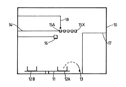
The apparatus shown in Figure 1 comprises a low
pressure chamber 10 which contains all items of coating
equipment. During use the chamber 10 is evacuated to 10 6
torr (i.e. 133 micropascals). The chamber 10 is
constructed to withstand this vacuum. Conventional
control and electric power lines pass in and out of the
chamber 10 but these are not shown in the drawing.
The source of coating takes the form of a
rotatable carousel 11, controllable from outside chamber
10, upon which copper hearths 12A and 12B, containing
1203 (to make the interlayer) and Gd203 (to make the
effect coating) respectively, are located. The chamber 10
also contains an electron gun 13 to generate an electron
beam which is focussed by magnets (not shown) onto the
hearth in the active position (i.e. hearth 12A as shown).
The hearths are loaded into chamber 10 by means not shown
in the drawing.
The chamber also contains a target holder 14
into which a plurality of targets 15A-15X, i.e. lasers in
this example, can be located. Each target is orientated
with the desired facet for coating downwards and a second
facet, passive in thi~ process, upwards. Coating is
uniform for all targets in a useable zone which is large
enough to contain up to 60 separate targets if desired.
Thus, withln the acceptable tolerance limits, the chamber
10 can be used to coat 60 items in a single batch.
As well as the targets 15 the chamber 10
contains a ~uartz crystal 16 which is also mounted in the
useful zone. The crystal 16 is used to monitor the
thickness of coatings. There is also a shutter 17,
controllable from outside the chamber, which can be
interposed in the beam to prevent deposition (e.g. at the
end of the process) on the targets 15 and the crystal 16.
In addition to the crystal 16 one of the
targets, namely 15A, is associated with a radiation sensor
18 positioned to receive radiation from the passive facet.
Target 15A is provided with excitation means not shown in
the drawing.
In use a plurality of indium-gallium arsenide-
phosphide lasers were mounted in holder 14 and hearths 12A
and 12B were placed in position. After the chamber had
been evacuated, the electron beam was switched on. This
evaporated A1203 which condensed on all the targets 15 to
produce the interlayer. The A1203 also deposited on
crystal 16. When 20 nm of A1203, as indicated by ~uartz
crystal 16, had deposited ~on all the targets) the hearths
12A and 12B were interchanged. This placed the Gd203 in
the electron beam whereby this compound evaporated and
_ ~ 71 ~3~
condensed on all targets to produce the effect coating.This coating was terminated at maximum effect as monitored
by sensor 18. The two monitoring processes will now be
described. Crystal 16 is caused to oscillate and the
S frequency of its oscillation is monitored outside the
chamber. Since the crystal is in the useful zone, vapour
from the hearth-in-use condenses on it to give a coating
of the same thickness as on all targets. The presence of
the coating affects the frequency of oscillation of the
crystal 16 and, by using a calibrated crystal, the
frequency shift provides an instantaneous measure of the
thickness of coating on the crystal whereby the growth of
the coating on the crystal 16 can be followed. Since the
thickness of the coating on the crystal 16 is the same as
the thickness on all the targets 15, the thickness of the
coating of A1203 on the targets can be controlled to 20
nm.
The sensor 18 provides a control which is
directly related to the performance of the target 15A.
Thus, if the laser 15A is subjected to constant
excitation, a constant amount of radiation is produced.
Thi~ constant amount leaves via the intended and passive
facets. The purpose of the effect layer i8 to obtain
maximum emission at the intended face and this corresponds
to minimum emission at the passive face (as recorded by
sensor 18).
Figure 2 shows the intensity which would be
recorded at constant excitation by sensor 18 on coating
from zero thickness up to w/2 thickness where w is the
wavelength of the radiation in the coating.
As can be seen the intensity remains constant
for very thin layers and then it falls to a minimum at
w/4. For thicker coatings the intensity recorded by
sensor 18 increases until it returns to its original value
at w/2. The optimum end point for the coating is at w/4.
Thus the "best" process would comprise depositing Gd203
until the sensor 18 gives a minimum reading and
terminating the deposition at the exact minimum. However,
~` 1~71~33~3
.
- 5 -
the precise minimum is hara to detect and, to make sure it
is reached, we prefer to overshoot by a negligible amount.
Thus we prefer to terminate as soon as a rising intensity
is noticed, (The changes of intensity indicated by Figure
2 are beyond the capacity of most detectors. This gives
rise to a difficulty which can be overcome by increasing
the excitation current to compensate for a low intensity.
A series of stepwise increases is preferred).
Using the techniques outlined above an indium-
gallium arsenide-phosphide laser was given an effect
coating of Gd203 200 nm thick with an interlayer of A1203
20 nm thick. The deposition of the A1203 was controlled
by quartz crystal 16. The Gd203 was coated to optimum
thickness as indicated by passing the minimum displayed by
sensor 18, i.e. using the technique described above.
It was found that this coating suppressed laser
activity to such an extent that it was not practical to
a~ess reflectivities or assign a laser threshold.
'~ For routine production, it is suggested that the
thickness of the effect coating also be controlled by
quartz crystal 16, as is conventional. However the quartz
crystal 16 is calibrated, using sensor 18 as described
above, so that the optimum th$ckness corresponding to
minimum reflectivity is applied.
!