Note: Descriptions are shown in the official language in which they were submitted.
71839
-- 1 --
s P E C I F I c A T I O N
T I T L E
"COMB FILTER, CHROMINANCE AND LUMINANCE SIGNAL SEPARATING
CIRCUIT FOR MODIFYING THE LEVEL-FREQUENCY CHARACTERISTIC
OF THE LUMINANCE SIGNAL"
BACKGROUND OF THE INVENTION
Field of the Invention
The present invention relates generally to color
video signal processing circuits, and more particularly,
is directed to a circuit for obtaining individually a
chrominance signal which is separated from a color video
signal and a luminance signal which is separated also
from the color video signal and modified to have a
predetermined level-frequency characteristic.
Description of the Prior Art
In a recording circuit arrangement employed in a
video tape recorder (VTR), luminance and chrominance
signals are separated respectively from a color video
signal which is supplied, for example, through a color
television broadcast. The separated luminance signal is
used for frequency-modulating an appropriate carrier to
produce a frequency-modulated luminance signal. The
separated chrominance signal is frequency-converted to
have a frequency band lower than the frequency band of
the frequency-modulated luminance signal. Then, the
frequency-modulated luminance signal and the frequency-
converted chrominance signal are mixed or combined to
form a composite video signal which is supplied to a
rotary magnetic head device to be recorded on a magnetic
tape.
For each of such separations of the chrominance and
luminance signals from the color video signal, a so-
called comb-filter is ordinarily used. In the case where
a color video signal according to the NTSC system
,i~
~:71839
-- 2
is processed, a subtraction-type comb-filter which
includes a delay device providing a signal delay of one
horizontal period (hereinafter, referred to as a lH
delay device) is used for separating the chrominance
signal from the color video signal. An addition-type
comb-filter which also includes the lH delay device is
used for separating the luminance signal from the color
video signal. To obtain the chrominance signal
components contained in the color video signal, the
subtraction-type comb-filter is formed to have a toothed
band pass characteristic which provides a minimum gain
for signal components residing in a frequency band lower
than the frequency band of the chrominance signal in the
color video signal, a depression falling into a minimum
gain at each frequency represented by N X fH, where N is
a positive integer and fH is a horizontal frequency, and
a peak reaching to a gain of zero decibels (hereinafter,
re~erred to as OdB) at each frequency represented by (N
+ l/2) X fH for signal components residing in the
frequency band of the chrominance signal components in
the color video signal.
To obtain the luminance signal contained in the
color video signal, the addition-type comb-filter is
formed to have another toothed band pass characteristic
which provides a gain of OdB for the signal components
residing in a frequency band lower than the frequency
band of the chrominance signal in the color video
signal, a peak reaching to a gain of OdB at each
frequency represented by N X fH and a depression falling
into a minimum gain at each frequency represented by (N
+ 1/2) X fH for the signal components residing in a
frequency band of the chrominance signal in the color
video signal.
In a reproducing circuit arrangement of the video
tape recorder, the frequency-modulated luminance signal
1;~71~339
-- 3 --
and the frequency-converted chrominance signal are
separated through a high pass filter and a low pass
filter respectively from the composite video signal
which is reproduced by the rotary magnetic head device
from the magnetic tape. Then, a reproduced luminance
signal is obtained by frequency-demodulating the
frequency-modulated luminance signal separated from the
reproduced composite video signal and a reproduced
chrominance signal is obtained by frequency-converting
the frequency-converted chrominance signal separated
from the reproduced composite video signal to cause the
same to reside in its original frequency band. The
reproduced luminance and chrominance signals are
combined with each other to be derived from an output
terminal as a reproduced color video signal.
The reproduced color video signal thus obtained
from the video tape recorder is supplied to, for
example, a color video monitor having an image display
device such as a color cathode ray tube. In the color
video monitor, chrominance and luminance signals are
separated from the reproduced color video signal
respectively through subtraction-type and addition-type
comb-filters having their respective toothed band pass
characteristics similar to those described above. That
is, in the event of a color video monitor for an NTSC
system color video signal, a subtraction-type comb-
filter which includes a lH delay device and a toothed
band pass characteristic which provides a depression
falling into a minimum gain at each frequency
represented by N X fH and a peak reaching to a gain of
OdB at each frequency represented by (N + 1/2) X fH for
the reproduced color video signal, is used for
separating the chrominance signal from the reproduced
color video signal. An addition-type comb-filter which
includes the lH delay device and a toothed band pass
" 1~ 7 ~ ~3~
characteristic which provides a peak reaching to a gain
of OdB at each frequency represented by N ~ fH and a
depression falling into a minimum gain at each frequency
represented by (N + 1/2) X fH for the reproduced color
video signal, is used for separating the luminance
signal ~rom the reproduced color video signal.
~ ssume the case where the luminance signal is
obtained through the addition-type comb-filter provided
in the recording circuit arrangement of a video tape
recorder. The comb-filter has a toothed band pass
characteristic which provides a constant gain of OdB for
the signal components residing in a frequency band lower
than the frequency band of the chrominance signal in the
color video signal, as described above, and therefore
has a constant level in a frequency band lower than the
frequency band of the chrominance signal. When such a
luminance signal is contained in the reproduced color
video signal which is supplied to the color video
monitor, there is the problem that the luminance signal
separated from the reproduced color video signal through
the addition-type comb-filter provided in the color
video monitor has signal components of frequencies
coinciding with each frequency represented by (N + 1/2)
X fH and their vicinities which are considerably
attenuated compared with other signal components
thereof. Such attenuated signal components of the
luminance signal separated from the reproduced color
video signal give rise to a deterioration in the quality
of the reproduced picture which is obtained by the color
video monitor based on the luminance and chrominance
signals separated from the reproduced color video
signal.
For compensating for the attenuation of the
luminance signal brought about in the color video
monitor as mentioned above, the luminance signal should
71~33~3
preferably contain signal components which are of
frequencies between each successive two of the
frequencies represented by N X fH and which are
emphasized in level within a predetermined frequency
band. A level control circuit can be used for
emphasizing the levels of selected signal components of
the luminance signal separated from the color video
signal in the recording circuit arrangement of the video
tape recorder. However, when a level control circuit is
provided in addition to the comb-filter and the level
control circuit contains a lH delay device which is in
addition to the lH delay device contained in the comb-
filter, the configuration of the recording circuit
arrangement of the video tape recorder is made
complicated and the production cost of the video tape
recorder is undesirably increased.
OBJECTS AND SUMMARY OF THE INVENTION
Accordingly, it is an object of the present
invention to provide a color video signal processing
circuit suitable for use in a video tape recorder, which
avoids the aforementioned problems encountered with the
prior art.
More particularly, it is an object of the present
invention to provide a color video signal processing
circuit operative to separate chrominance and luminance
signals from a color video signal, which is relatively
simple in construction without any particular delay
device other than a delay device used for signal
separation, and by which the chrominance signal is
separated individually from the color video signal and
the luminance signal is also separated individually from
the color video signal and modified to have a
predetermined level-frequency characteristic.
~183~3
-- 6 --
Another object of the present invention is to
provide a color video signal processing circuit for
separating chrominance and luminance signals from a
color video signal, which is relatively simple in
construction and without any particular delay device
other than a delay device used for signal separation. A
luminance signal containing signal components which are
of frequencies between each successive two of the
frequencies represented by N X fH and emphasized in
level within a predetermined frequency band must be
obtainable as the luminance signal separated from the
color video signal together with the chrominance signal
also separated from the color video signal.
According to the present invention, there is
provided a color video signal processing circuit for
separating chrominance and luminance signals from a
color video signal, the circuit comprising: an input
terminal for receiving the color video signal, signal
separating means, including first and second
intermediate terminals, delay means for delaying the
color video signal supplied through said input terminal
by at least substantially one horizontal period, a
subtraction-type comb-filter, including said delay
device, connected between said input terminal and said
first intermediate terminal, and an addition-type comb-
filter, also including said delay device, connected
between said input terminal and said second intermediate
terminal, whereby a signal Cy containing the chrominance
signal as a major component and the luminance signal as
a minor component is generated at said first
intermediate terminal and a signal Yc containing the
luminance signals a major component and the chrominance
signal as a minor component is generated at said second
intermediate terminal. Further included are level
modifying means connected to said first intermediate
127~83~3
terminal for outputting a signal which emphasizes the
level of a first segment of the Cy signal residing in a
predetermined frequency band lower than the frequency
band of the chrominance signal and attenuating the level
of a second segment of the Cy signal residing in the
frequency band of the chrominance signal, adding means
for adding the output of said level modifying means to
said Yc signal obtained at said second intermediate
terminal and outputting the result, first output means
for deriving a separated chrominance signal from said
first intermediate terminal, and second output means for
deriving a separated luminance signal from said adding
means.
In the circuit thus constituted in accordance with
the present invention, a first partial circuit
arrangement is connected between the input terminal and
the first intermediate terminal and has a first toothed
band pass characteristic which provides a depression
falling into a minimum gain at each frequency
represented by N X fH and a peak reaching to a gain of
OdB at each frequency represented by (N + l/2) X fH or
(N + 1/4) X fH for the color video signal supplied
through the input terminal. A second partial circuit
arrangement is connected between the input terminal and
the second intermediate terminal and has a second
toothed band pass characteristic which provides a peak
reaching to a gain of OdB at each frequency represented
by N X fH and a depression falling into a minimum gain
at each frequency represented by (N + 1/2) X fH or (N +
1/4) X fH for the color video signal supplied through
the input terminal. Further, a third partial circuit
arrangement is connected between the input terminal and
the output end of the level modifying portion and has a
third toothed band pass characteristic whish provides a
depression falling into a minimum gain at each frequency
, . , , ~ ,
339
represented by N X fH and a peak reaching to a gain more
than ods at each frequency represented by (N + 1/2) X fH
or (N + 1/4) X fH for signal components of the color
video signal residing in a predetermined frequency band
lower than the frequency band of the chrominance signal.
A fourth partial circuit arrangement is connected
between the input terminal and the output end of the
adding portion and has a fourth toothed band pass
characteristic which provides a depression falling into
a gain of OdB at each frequency represented by N X fH
and a peak reaching to a gain more than OdB at each
frequency represented by (N + 1/2) X fH or (N + l/4) X
fH for the signal components of the color video signal
residing in a predetermined frequency band lower than
the frequency band of the chrominance signal. The "N"
is a positive integer in each case above.
With these first to fourth partial circuit
arrangements having the above-described first to fourth
toothed band pass characteristics, respectively, the
separated chrominance signal and the separated luminance
signal containing its signal components which are of
frequencies between each successive two of the
frequencies representèd by N X fH and which are
emphasized in level within a predetermined frequency
band lower than the frequency band of the chrominance
signal in the color video signal are obtained through
the first output portion and the second output portion,
respectively, using a relatively simple circuit
configuration without any particular delay device other
than the delay device used in common for forming the
subtraction-type and addition-type comb-filters.
The above, and other objects, features and
advantages of the present invention will become apparent
from the following detailed description which i6 to be
read in conjunction with the accompanying drawings.
... . .
~'~71~339
BRIEF DESCRIPTION OF THE DRAWINGS
Fig. 1 is a block diagram showing one embodiment of
color video signal processing circuit according to the
present invention; and
Figs. 2A to 2E are diagrams showing the frequency
characteristics of the partial circuit arrangements in
the embodiment shown in Fig. 1.
DESCRIPTION OF THE PREFERREDEMBODIMENT
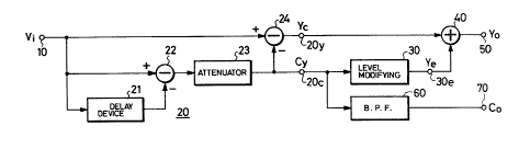
Fig. 1 shows an embodiment of color video signal
processing circuit according to the present invention,
which i5 operative to separate chrominance and luminance
signals individually ~rom a color video signal generated
in accordance with the NTSC system.
Referring to Fig. 1, an input color video signal
Vi, including chrominance and luminance signals
according to the NTSC system, is supplied through an
input terminal 10 to a signal separating portion 20
containing a lH delay device 21 which delays the input
color video signal Vi by one horizontal line period.
The signal separating portion 20 is constituted to fo~m
both a subtraction-type comb-filter, including the lH
delay device 21, between the input terminal 10 and a
first intermediate terminal 20c, and an addition-type
comb filter, including also the lH delay device 21,
between the input terminal 10 and a second intermediate
terminal 20y. That is, in the signal separating portion
20, the input color video signal Vi is supplied directly
to the (+) input of a first subtracter 22 and through
the lH delay device 21 to the (-) input of the first
subtracter 22. The output of the first subtracter 22 is
supplied to an attenuator 23 where it is attenuated in
level by a factor of one half. The output of the
attenuator 23 is supplied to the first intermediate
. :,, ''' :- . ....
~'~71~3'3
-- 10 --
terminal 20c and also supplied to the (-) input of a
second subtracter 24 having its (+) input supplied
directly with the input color video signal Vi. The
output of the second subtracter 24 is supplied to the
second intermediate terminal 20y.
The circuit arrangement in the signal separating
portion 20 connected between the input terminal 10 and
the first intermediate terminal 20c has the toothed band
pass characteristic shown in Fig. 2A where fsc indicates
the color subcarrier frequency and n and _ are positive
integers respectively. This toothed ~and pass
characteristic provides a depression falling into a
minimum gain at each frequency represented by N X fH and
a peak reaching to a gain of OdB at each frequency
represented by (N + 1/2) X fH for the input color video
signal Vi. The circuit arrangement in the signal
separating portion 20 connected between the input
terminal 10 and the second intermediate terminal 20y has
the toothed band pass characteristic shown in Fig. 2B
which provides a peak reaching to a gain of OdB at each
frequency represented by N X fH and a depression falling
into a minimum gain at each frequency represented by (N
+ 1/2) X fH for the input color video signal Vi.
Consequently, a signal Cy containing the
2S chrominance signal as a major component and the
luminance signal included as a minor component in the
chrominance signal is obtained at the first intermediate
terminal 20c, and another signal Yc containing the
luminance signal as a major component and the
chrominance signal included as a minor component in the
luminance signal is obtained at the second intermediate
terminal 20y. The luminance signal contained in the
signal Yc has signal components which are of frequencies
between each successive two of the frequencies
represented by (N + 1/2) X fH and they are considerably
339
attenuated compared with other signal components
thereof.
In this embodiment, the frequency band below the
frequency band of the chrominance signal in the input
color video signal Vi is divided into a low range of OHz
to lMHz, a middle range of lMHz to 2MHz, including a
frequency nfH at the central portion thereof, and a high
rang of 2MHz to the lowest frequency fL in the frequency
band of the chrominance signal, including a frequency
mfH at the central portion of this high range. It is
desired to obtain a luminance signal, separated from the
input color video signal Vi, which contains signal
components which are of the frequencies between each
successive two o~ the frequencies represented by N X fH
and which are emphasized in level within the middle
range o~ lMHz to 2MHz.
A level modifying portion 30 is connected to the
first intermediate terminal 20c and receives the signal
Cy obtained therefrom. The level modifying portion 30
has a frequency characteristic as shown in Fig. 2C which
provides a gain of OdB for signal components of the
signal Cy residing in the low range of OHz to lMHz, a
gain of more than OdB for signal components of the
signal Cy residing in the middle range of lMHz to 2MHz,
and a minimum gain for signal components of the signal
Cy residing in the high range of 2MHz to the lowest
~requency fL in the frequency band of the chrominance
signal. Such a level modifying portion 30 may comprise
a low pass filter which has a cut-off frequency of 2MHz
and is modified to provide an increased gain for the
signal components of the signal Cy residing in the
t middle range of lMHz to 2MHz.
Accordingly, the circuit arrangement provided
between the input terminal 10 and an output end 30e of
the level modifying portion 30 has a toothed band pass
~2~39
- 12 -
characteristic as shown in Fig. 2D which provides a
depression falling into a minimum gain at each frequency
represented by N X fH and a peak reaching to a gain of
OdB at each frequency represented by (N + 1/2 ) X fH for
the signal components of the signal Cy residing in the
low range of OHz to lMHz, a depression falling into a
minimum gain at each frequency represented by N X fH and
a peak reaching to a gain of more than OdB at each
frequency represented by (N + 1/2) X fH for the signal
components of the signal Cy residing in the middle range
of lHz to 2MHz, and a minimum gain for the signal
components of the signal Cy residing in the high range
of 2MHz to the lowest frequency fL in the frequency band
of the chrominance signal. Thus a narrow-band luminance
signal Ye which includes first signal components thereof
residing in the middle range of lHz to 2MHz and second
signal components thereof residing in the middle range
of lHz to 2MHz and emphasized compared with the first
signal components is obtained at the output end 30e of
the level modifying portion 30.
The narrow-band luminance signal Ye is
added by an adder 40 to the signal Yc obtained from the
second intermediate terminal 20y and a separated
luminance signal Yo is supplied from the adder 40 to a
luminance signal output terminal 50.
As a result of the above described construction, a
the circuit arrangement provided between the input
terminal 10 and the luminance signal output terminal 50
has a toothed band pass characteristic as shown in Fig.
2E which provides a constant gain of OdB for signal
components of the input color video signal Vi residing
in the low range of OHz to lMHz, a depression falling
into a gain of OdB at each frequency represented by
N X fH and a peak reaching to a gain of more than OdB at
each frequency represented by (N ~ 1/2) X fH for signal
3~
- 13 -
components of the input color video signal Vi residing
in the middle range of lHz to 2MHz, and a peak reaching
to a gain of ods at each frequency represented by N X fH
and a depression falling into a minimum gain at each
frequency represented by (N + l/2) X fH for signal
components of the input color video signal vi residing
in the high range of 2MHz to the lowest frequency fL in
the frequency band of the chrominance signal.
Therefore, the separated luminance signal Yo obtained at
the luminance signal output terminal 50 has signal
components which are of the frequencies between each
successive two of the frequencies represented
by N X ~H and emphasized in level within the middle
range of lMHz to 2MRz.
The signal Cy obtained at the first intermediate
terminal 20c is supplied to a band pass filter (B.P.F)
60 which has a pass band coinciding substantially with
the frequency band of the chrominance signal in the
input color video signal Vi and a separated chrominance
signal Co is outputted from the band pass filter 60 to a
chrominance signal output terminal 70.
Accordingly, the circuit arrangement provided
between the input terminal lO and the chrominance signal
output terminal 70 has a toothed band pass
characteristic which provides a minimum gain for signal
components of the input color video signal Vi residing
in a frequency band lower than the frequency band of the
chrominance signal in the input color video signal Vi,
and a depression falling into a minimum gain at each
frequency represented by N X fH and a peak reaching to a
gain of OdB at each frequency represented by (N + l/2) X
fH for signal components of the input color video signal
Vi residing in the frequency band of the chrominance
signal.
~ 7i ~3
Although the separated chrominance and luminance
signals Co and Yo are obtained from the color video
signal according to the NTSC system in the above
described embodiment and therefore a lH delay device 21
is used for the signal separating portion 20, it is to
be understood that a 2H delay device which provides a
signal delay of two horizontal periods may be used for
the signal separating portion 20 in place of the lH
delay device 21 so as to allow the circuit according to
the present invention to be applied for separating
chrominance and luminance signals individually from a
color video signal according to the PAL system. In such
event, the circuit arrangement in the signal separating
portion 20 provided between the input terminal 10 and
the first intermediate terminal 20c has a toothed band
pass characteristic which provides a depression falling
into a minimum gain at each frequency represented by
N X fH and a peak reaching to a gain of OdB at each
frequency represented by (N + 1/4) X fH for the color
video signal according to the PAL system, and the
circuit arrangement in the signal separating portion 20
provided between the input terminal 10 and the second
intermediate terminal 20y has another toothed band pass
characteristic which provides a peak reaching to a gain
of OdB at each frequency represented by N X fH and a
depression falling into a minimum gain at each frequency
represented by (N + 1/4) X fH for the color video signal
according to the PAL system.
Although the present invention has been shown and
described with respect to preferred embodiments, various
changes and modifications which are obvious to a person
skilled in the art to which the invention pertains are
deemed to lie within the spirit and scope of the
invention.