Note: Descriptions are shown in the official language in which they were submitted.
1~:7~9~
METHOD AND APPARATUS FOR CONVERTING AN ANALOG SIGNAL
TO A DIGITAL SIGNAL USING AN OVERSAMPLING TECHNIQUE
BACKGROUND OF THE INVENTION
This invention relates to an oversampled analog-to-
digltal (A/D) converting method and apparatus capable of
achieving precise coding.
Oversampled coders sample an analog signal at a higher
frequency than the Nyquist frequency, quantize the sampled
slgnal, and perform the bandlimltation and reduction of the
sampling frequency to produce a coded output. For details
of the oversampled coder, reference is made to an article
by Stuartk K. Tewksbury et al., entitled "Oversampled,
Linear Predictive and Noise-Shaping Coders of Oder N ~ 1",
published in the IEEE Transactions On Circuits And Systems,
Vol. CAS-25, No. 7, July issue, 1978, pp. 436 - 447 Since
the above-mentioned oversampled coder may be composed of
only digital circuits with exception of a low resolution
digital-to-analog (D/A) converter and an integrator, the
coder is suitable for a large scale integration circuit
(LSI).
With a view to minimizing the whole device as well as
to lowering power consumption and the manufacturing cost
of the device, it is necessary not only to simplify the
analog structural elements used but also to reduce the
d
1~:71~5
66446-342
number of operations per unlt time in the digital structural
elements used. For this purpose, it is desirable that simple
operations are performed at a high sampling frequency, while
complicated ones, at a low sampling frequency.
SUHHA~Y OF THE DVE~ION
It is, therefore, an ob~ect of the invention to provide
a method and apparatus for A/D conversion using an oversampling
technique to achieve high precision linear coding.
It is another objeGt of the invention to provide a
method and apparatus for A/D conversion enabling a digital circuit
operable at a high frequency to be simplified.
It is still another object of the invention to provide a
method and apparatus for A/D conversion suitable for LSI's.
According to one aspect of the invention, there is
provided an oversampled analog-to-digital conversion method
comprising the steps of.
(A) oversampling an input analog signal at a first frequency
higher than the Nyquist frequency to produce a sampled signal;
(B) subtracting a local decoded signal from the sampled
signal;
(C) quantizing the subtracted signal into a quantized binary
signal;
(D) generating said local decoded signal by integration of
the quantized binary signal;
(E) converting the quantized binary signal havlng the first
frequency into a frequency-reduced signal having a second
frequency, said converting step further including,
._ .,
. '.'!. . :.: . L. ' ""
~71~395
66446-342
(a) generating a plurality of coefficient groups each of
which has a plurality of coefficients,
(b) performing in response to said quantized binary signal
an addition or subtracting of each coefficient belonging to said
each group for every group to produce a processed result for every
group,
(c) accumulating the processed result for every group to
produce an accumulater result for every group, and
(d) producing said frequency-reduced signal based on said
accumulated result for every group; and
(F) integrating the frequency-reduced signal at the second
frequency to provide a converted digital signal.
Accordlng to the invention, there i6 also provided an
oversampled analog-to-digital converter comprising:
(A) means for sampling an input analog signal at a first
frequency higher than the Nyquist frequency to produce a sampled
signal;
(B) subtracting means for subtracting a local decoded signal
from the æampled signal;
(C) quantizing means for quantlzing the output of the
subtracting means to produce a quantized binary signal having a
first frequency;
(D) means for integrating the guantized binary signal to
generate the local decoded signal;
(E) converting means for converting the quantized binary
signal having the first frequency-reduced signal having a second
frequency, said converting means further including2
,, , ~ .. _~
~ , .
~71~3~3~
66446-342
(a~ coefficient generatlng means for generating a plurality
of coefficient groups each of which has a plurality of
coefficient,
Ib) processing means responsive to said quanti~ed binary
signal for performing an addition or subtraction of each
coefficient belonging to said each group of every group to produce
a processed result for every group,
(c) accumulating means for accumulating the processed result
for every group to produce an accumulated result for every group,
and
(d) means for producing said frequency-reduced signal based
on sald accumulated result for every group; and
(F) integrating mean~ for integrating the frequency-reduced
signal at the second frequency to provide a converted digital
signal.
BRIEP DESCRIPTION OF THE DRAWINGS
The invention will be described more in detail with
reference to the accompanying drawings:
Figure 1 is a block diagram showing a prior art
oversampled A/D converter;
Figures 2A through 2F are waveform diagrams for
describing the operation of the converter shown in Flgure 1;
3a
,. ..
Fig. 3 is a block diagram of an embodiment of the
invention;
Fig. 4 is a block diagram showing a sampling frequency
converter used in the embodiment;
Figs. 5 and 6 are digital filters used in the
invention;
Figs. 7 and 9 are circuit diagrams showlng the
detailed structures of the sampllng frequency converter;
and
Figs. 8A through 8L and Figs. 10A through 10I are
time charts for describing the operation of the sampling
frequency converters shown in Figs. 7 and 9.
Like reference numerals denote like structural
elements.
DESCRIPTION OF THE PRIOR ART
For easier understanding of the invention, a prior
art oversampled A/D converter (referred to as a
oversampled coder) will be described with reference to
Fig. 1 and Figs. 2A to 2F.
Referring to those drawings, an input analog signal
applied to an input terminal 1 is assumed to have a
frequency band of about fB(Hz) as shown in Fig. 2A.
The input signal is converted into a sampled signal by
a sampling switch 11 which operates at a higher sampling
frequency fH than the Niquist sampling frequency, 2fB.
-- 5
A subtracter 12 subtructs a local decoded analog signal
from the samp~d signal to produce an error signal. The
error signal is integrated by a noise-shaping integrator 13
to produce an integrated slgnal. Another subtracter 14
subtracts the local decoded signal from the integrated
signal to supply the difference to a two level quantizer 15.
The quantizer 15 discriminates a sign of the output of
the subtracter 14 and produces + ~ or ~ ~ based on the
discriminated positive or negative sign. A predictive
integrator 16 integrates the quantized output to produce
a local decoded digital signal (Fig. 2B!, which is
converted into a local decoded analog signal by a D/A
converter 17. Assuming that a sampling interval
T = l/fH and Z = exp(sT), the integrators 13 and 16 have,
in Z plane, system functions represented by 1/(1 _ z 1)
and z 1/(1 _ z 1), respectively. The integrator 13 or 16
can be realized with an adder 131 or 161 and a delay
circuit 132 or 162 having one sample delay.
The coded signal having the sampling frequency fH
given from the integrator 16 is then converted into a
signal having the Nyquist sampling frequency fs(= 2 x fB).
In the oversampled coder shown in F_g. 1, the sampling
frequency fH is reduced to the sampling frequency fs
through the intermediate sampling frequency fM. It is
noted that fM is defined as fH > fM > fs~ and that
fH/fM = M and fM/fs = N are chosen to be integnal numbers.
3 ~71~
-- 6
A digital FIR filter 18 is used to eliminate the
quantization noise around a frequency integral multiple
of the frequency fM prior to the sampling frequency
reduction. The filter 18 is preferred to have the
characteristic shown in Fig. 2C. When the output of the
filter 18 is resampled at the frequency fM by the
sampling switch 19, the spectrum repeated at the frequency
fM is obtained as shown in Fig. 2D.
A digital IIR filter 20 is a low-pass filter with
the frequency band about fB operable at the sampling
frequency fM and has the frequency characteristic shown
in Fig. 2E. The filter 20 is combined with the fllter 18
so that the inband frequency characteristic is flat.
By passing through the filter 20, the quantization noise
and the frequency components of the less than fM ~ fB(HZ)
are suppressed sufficiently. The output of the filter 20
is then resampled by the sampling switch 21 to produce
the signal with the sampling frequency fs (Fig. 2F).
In the oversampled coder of Fig. 1, the predictive
integrator 16 and filter 18 perform a high-speed operation.
The integrator 16 which merely accumulates the output
(+~) of the quantizer 15, may consist of an up-down
counter or a reversible counter. On the other hand,
the digital FIR filter 18 having a complicated circuit
structure may be composed of an accumulator which
repeatedly performs the addition M (= fH/fM) times to
~L~71~
- 7 - .
avoid such a complicated operation This means that a
digital filter has M coefficients, each of which is
assumed to be "1". In the construction like this, however,
the attenuation of the frequency about integral multiples
of fM(Hz) is not always sufficient, and the quantization
noise involved in the signal band becomes large due to
the reduced sampling frequency.
The invention solves the above-mentioned problems
by supplying a binary signal to the digital FIR filter,
thereby making the multiplication required in the digital
FIR filter unnecessary.
The princlple of the invention will be described
in detail. When W(z) represents the z-transform of the
output signal of the quantizer 15, W(z) is expressed as
follows:
W(z) = -l)x(z) + (1 _ z 1) Q(z)
For obtaining X(z) from the equation, it is necessary to
multiply X(z) by 1/(1 _ z 1) in the process of reducing
the sampling frequency. In the present invention, the
operation of 1/(1 ~ z 1) is transformed as follows:
1 1 +z-l + z-2 + z~3 + + z-(M-l) 1
-1 ~ -M ~ ( )
The numerator on the right side of the equation (1) indicates
a polynomial in respect to z 1 and a transfer function of
~c:71~
-- 8
an M-tap digital FIR filter operable at the sampling
frequency fH. On the other hand, the denominator on
the right side represents a polynomial as to z M, and
the operation of 1/(1 _ z M) is equal to the transfer
function of the integrator havlng a sampling frequency
of fH/M = fM. Accordingly, the operation of 1/(1 _ z M)
can be executed after the sampling frequency f~ has been
reduced to the frequency fM. Furthermore, the numerator
on the right side may be incorporated with the transfer
function of the fllter,l~to ~evelop a single digital FIR
filter. If the number of taps of the filter 18 is
~L + 1), the incorporation of the filter 18 with the
numerator of the right term of equation (1) corresponding
to the M-tap filter gives a synthetic digital FIR filter
having (M + L) taps. Thus, when the synthetic FIR filter
decreases the sampling frequency from fH to fM and an
integrator operable at the low frequency fM performs the
operation of 1/(1 _ z M), an A/D converted signal is
obtained. The number of tap~ (M + L) of the synthetic
filter is chosen to be an integral multiple of the
reduction ratio fH/fM = M. Herein the number of taps,
(M + L), may include a tap having a coefficient of value
= 0 and it may be an end tap. Assuming that the synthetic
filter having (M + L) taps has coefficients h(0), h(l),
...., and h(M + L - 1), an input signal sequence is x(n),
and filter output is y(n), the output y(n) is given by
the following equation:
.,
~ 7~ ~5~
g
M+L-l
y(n) = ~ h(k)x(n - k) (2)
k=0
Since the filtex output is decimated by M, the output
y(n) is calculated at intervals of M: y(0), y(M), y(2M),
...., and y(mM). ~sing mM = M + L, both y(0) and y(mM)
are calculated by the same hardware. In other words, as
understood from equation (2), the number o~ input samples
necessary to yield y(0) is M + L, and they are
x(~M - L + 1), x(-M - L + 2), ...., x(-l), and x(0),
respectively. Likewise, input samples necessary to yield
y(mM) are x(l), x(2), ...., and x(M + L), the number of
samples being M + L. The two sample sequences are
successive without overlapplng. Accordlngly, if there
ls provlded a devlce for computlng the equation (2), then
the computatlon of y(0), y(mMj, y(2mM), .... ls executed
by repeatlng the operatlon deflned by the equatlon (2).
Furthermore, it needs yielding serieses such as y(M),
y(M + mM), y(M + 2mM), ...., and y(2M), y(2M + mM) ....;
and thus it may be adequate that m devlces in total are
used and their outputs are summed up. As stated above,
since x(n) is binary of -+ ~, under the assumption
of /\ = 1, the calculation according to equation (2) is
achieved by a simple accumulation.
DESCRIPTION OF THE PREFERRED EMBODIMENTS
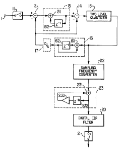
Fig. 3 shows an embodiment of the invention in which
~ ~71~3~35
-- 10 --
reference numerals 1,11, 12, 13,
14, 15, 16, 17, 20, 21, 131, 132, 161, and 162 designates
components or elements corresponding to or having the
same function as those designated by the same reference
numerals in Fig. 1. In addition to these elements, the
embodiment comprises a sampling frequencing converter 22
for converting the quantized binary signal having the
sampling frequency fH given from the quantizer 15 into
a frequency reduced signal having a sampling frequency fM,
and an integrator for integrating the frequency reduced
signal at the frequency fM.
Referring to Fig. 4 showing the converter 22, the
binary quantized signal from the quantizer 15 is supplied
to delay circuits 2211, 2212, ...., and 221J (J = M + L - 1).
Since the quantized signal is binary + ~ or - ~, if + A
and -~ are allocated "1" and "0", respectively, then
each of the delay circuits can be realized by one bit
flip flop. A sampllng switch 222 takes out the (J + 1)
bits from the delay circuits,in response to the sampling
frequency fM supplied to a terminal 220, to produce a
binary signal having the frequency fM. Coefficient
circuits 2230, 2231, ...., and 223J produce a coefficient
hj or -hj (j = 0, 1, ..., J) in accordance with "0" or
"1" of the output of the sampling switch 222. Adders
2241, 2242, .... , and 224J summate outputs of all the
coefficient circuits. It follows that the amount of
~ 7~ ~,6~
operation necessary for the sampling frequency change is
only J-times additions (subtractions) per l/fM (seconds),
thereby making the multiplication of the coefficients
unnecessary. Also, each delay circuit made up of one
bit fllp flop contributes to achieving a remarkably
simplified circuit structure.
Referring back to Fig. 3, the output of the converter
22 is applied to the digital integrator 23. The integrator
23 comprises an adder 231, a delay circuit 232 having
delay of l/fM, and a multiplier 233 and executes the
operation of 1/(1 _ z M) in equation 1. The multiplier 233
performs the multiplication of a given input by ~ l to
bring the transfer function of the integrator 23 into
1/(1 - ~z ). On assuming ~ = 1, the inputs signal given
to the digital filter 20 is equal in the structures of
Figs. 1 and 3. Generally, however, the value of ,~ is
preferred to be a little smaller than 1, because the
value of ~ smaller than 1 reduces influence due to the
initial value of the delay circuit 232 with passage of
time.
Assuming that ~ 2 m (m ls integer) is established,
the multiplication of ~ can be simply reali~ed by a digit
shift of a binary signal and the subtraction.
Referrlng to Fig. 5 showing the digiral FIR filter 18,
the local decoded signal given from the integrator 16 is
delayed by one sample in delay circuits 811, 812, .....
~.~71~5
- 12 -
and 81M. The signals taken out of the respective delay
circuits are multiplied by ~lter coefficients hG, hl, .....
and hL in multipliers 820, 82], ...., and 82L. The outputs
of the multipliers are summed by adders 831, 832, .....
and 83L. The summed result is sent to the sampling
switch 19. The filter coefficients ho~ hl, ...., and hL
are derived from an impulse response of this filter, and
Z-transform of the impulse response and the frequency
characteristic are expressed as:
H(z) = ~0 hi Zi
H(eiW) = ~ h e-ji
i=O i
Referring to Fig. 6, the filter 20 performs the
operation determined with the fol~owing system function:
H(z ) = r~ aO(1+aljz +a2 jZ )/(1+ bljZ +b2jZ
where z M represents a sampling period of l/fM = M (l/fH).
Multipliers 900, 911, and 912, a subtracter 921, an adder
922 and delay circuits 931 and 932 execute the operation
of 1/(1 + bll z + b21 z M) in the system function H(z ).
Meanwhile,~the operation of 1/(1 + all z M + a21 z ) is
executed by multipliers 913, 914 and adders 923, 92~.
.
.. :
1;~71'~9S
- 13 -
Referring to Fig. 7 showing a detail structure of the
converter 22, the converter 22 comprises a counter 221,
read only memories (ROM's) 222l, 2222 and 2223, addition/
subtraction units (ASU's) 223l, 2232 and 2233, registers
2251, 2252 and 2253 for delaying by one sampling time.
The ROM 222i (i = l, 2, 3) stores the filter coefficients
of the (M + L) taps. The ASU 223i, register 224i and
switch 225i (i = l, 2, 3) constitute an accumulator
for accumulating the output of the ROM 222i. Herein is
lG shown an example consisting of three accumulaters under
the assumption of (M + L) = 3 x M.
Referring to Figs. &A through 8L, the operation of
the converter 22 shown in Fig. 7 will be described below.
A clock pulse at fH (bits/second) (Fig. 8A) applied
to a terminal 220 is subjected to (M + L) frequency
division by a counter 221. Fig. 8B shows contents of the
counter 221: 0, 1, 2, ...., and 17 when (M + L) is 18.
The ROM's 222l, 222~ and 2233 are addressed by the outputs
of the counter 221 to produce filter coefficients hl7,
hl6, hl5, ...., and ho. The ~ddresses of the ROM's are
set to correspond with deviation of M(= 6) to the
coefficients. More specifically, when the ROM 2221
outputs the coefficient ho~ the ROM 2222 outputs the
coefficient h6. Likewise, when ~e ROM 2222 outputs the
25 coefficient ho~ the ROM 2223 outputs coefficient h6.
Furtherfore, when the ROM 2223 output the coefficient h
~:7~95
- 14 -
the ROM 2221 outputs the coefficient h6. These relationship
are shown in Figs. 8C to 8E. In these drawings, reference
numerals represent the subscripts of the coefficients hk.
The output of the ROM 222i is added to or subtracted
from the output of the register 224i (Figs. &F to 8H).
As shown ln Figs. 8C to 8H, when the ROM 222i produces
the coefficient hl7, the output of register 224i is
always "0". Whether the ASU's should perform addition or
subtraction depends on the quantized output + ~ from the
quantizer 15. In the circuit shown in Fig. 7, the
addition is represented by +~, while the subtraction,
by - A. The ~t~ut~ the ASU 223i is applied to the
register 224i through a switch 225i. Figs. 8I through ~K
exhibit the pattern of operatlon of the switches 225
to 2253, in which digit "1" or "0" indicates the
connection to the register 224i or the integrator 23.
Since the switch 225i is connected to the integrator 23
upon the coefficient ho from the ROM 222i, "0" is supplied
to the register 224i. Therefore, at the next time slot
when the ROM 222i output the coefficient hl7, "0" is
output from the register 224i. In this way, the ROM 222
ASU 223i, register 224i and switch 225i perform the
operation expressed by:
htl7) x(n - 17) + h(16) x(n - 16) + .... + h(0) x(n)
It is noted that x(n - k) is a binary signal given from
the quantizer 15. The above operation is equivalent to
~ :' ,' '
.
1;:7~ 3~
- 15 -
equation (2), and thus the combination of three circuit
units as described above covers all necessary arithm~,etic
operation. Fig. 8L shows the converted signal whose
sampling frequency is decreased to one sixth.
Referring to Fig. 9, a ROM 2220 is addressed by the
content (Fig. 10) of a counter (CT) 2210 which is obtained
by frequency-dividing the clock pulse having fH (bit/second)
in (M + L) (Fig. 10A). The ROM 2210 receives an enabling
signal given at a terminal 232, obtained by frequency
dividing the clock of 3 x fH (bits/second) in three.
Accordingly, the ROM 2220 produces a filter coefficient
hk changing at every (3 x fH) 1 seconds (Fig. 10F).
This is equivalent to the time division multiplex of the
outputs of the ROM's 2221, 2222 and 2223 in Fig. 7.
The required capacity of the ROM 2220 is 3 x (M + L) words,
which is equal to the summation of the capacities of the
ROM's 2221, 2222 and 2223. This also means that three
ROM's 2221, 2222 and 2223 can be substituted by a single
ROM, which leads to the simplification of the circuit.
The same effect can be achieved by setting the capacity
of the ROM 2220 to (M + L) words, providing three address
generator, and time-division multiplexing the three
address signals. An ASU 2230 performs addition or
subtraction between the outputs of the ROM 2220 and a
switch 2250 (Fig. 10G). The quantized signal (Fig. 10H)
has the sampling frequency fH and is constant during
~;
. ~ .
71'~3S
- 16 -
three time slo~s. Theolt~ut~ t~e ASU 2230changes at every
(3 x fH) 1 seconds as shown in Fig. 10I. It follows that
the ASU 2230 can realize the operation of the ASU's 2231,
2232 and 2233 shown in Fig. 7 by the time-dlvision
multiplexing technique. Registers 2263, 2261 and 2262
store the output of the ASU 2230 in response to timing
pulses (1), (2) and (3) of fH (bits/second) (Figs. 10A
through 10C) applied to terminals 229 through 231. The
signal stored in the register 223i is supplied to a
swltch 2250 through a gate 227i. The gate 227i passes
the output of the register 223i in response to "1" of
the timing pulse (1), (2) or (3) to time-division
multiplex the output of the register 226i. The switch
225G connects the gate 227i to a buffer memory 228 to
give "0" to the ASU2230 at the time when the ROM 2220
outputs the coefficient hl7. The buffer memory 28 absorbs
time fluctuation of the gate's output changing within
(3 x fH) 1 seconds. The sampling frequency converter 22
shown ln Fig. 9 is the same in principle and function as
that shown in Fig. 7 though different in circuitry as
means for realization between them.
The invention enables the reduction of a sampling
frequency without needing complicated multiplication.
Though the two-step reduction of the sampling frequency
has been described with reference to Fig. 3, alternatively
is usable the method for directly reducing the sampling
~.~7~
- 17 -
frequency from fH to fs. This method requires an FIR filterhaving a frequency characteristic in which attenuation
is large in the out-of-band and gain deviation is small
in the inband. Such an FIR filter has remarkably large
number of taps and the coefficients complicated. ~n this
case, however, according to the invention, it can do
with only performing addition (subtraction) the number
of times corresponding to the number of taps during the
period of l/fs without needing multiplication.
The invention contributes to minimizing the total
device and lowering power consumption and the manufacturing
cost of an A/D converter.
The invention also provides the advantage that the
integrator 16 (Fig. 3) may be an analog integrator, with
the consequent omission of the D/A converter 17.