Note: Descriptions are shown in the official language in which they were submitted.
VARIABLE GAIN ENCODER APPARATUS AND METHOD
Field of the Invention
The invention is in the field of analog to digital
encoders and more particularly relates to a telephony encoder
with variable gain.
Backqround of the Invention
Telephone systems of the digital signal type require
analog to digital and digital to analog converter circuits,
usually referred to as CODECs for interfacing voice signals and
the like between analog signals compatible with analog
transducers and binary signals compatible with digital telephony
switching and transmission function and apparatus. In order
that the encoding function be performed such that pulse code
modulated (PCM) words are generated which accurately represent
an analog input signal, the analog signal must be centered about
an encoder midpoint. That is, the encoder operating midpoint
and the zero level of the analog signal should correspond. If
not, quantization distortion, harmonic distortion and noise are
included in the PCM words. It is typical practice to have
predetermined the gain of an encoder during manufacture, and if
desired, later when in use, alter the gain, in circuit, with the
use of a preset gain pad. Biasing of the midpoint may be
conveniently achieved by AC coupling an appropriate node within
the encoder and charging the node via a switched capacitor
resistance to null any offset at the encoder input. In effect,
the sign bit of each PCM word is integrated onto the AC coupled
1;~7~3~
node such that its long term voltage (d.c. value) is
representative of the average of the sign bit polarities.
Stability is achieved when the sign bit occurrences are evenly
negative and positive.
If however the gain of the typical encoder is changed
during its normal operation, a step component consequently
appears at the input of the encoder because the integrated
signal at the AC coupled node no longer cancels the total
offset. Hence, the operational midpoint is shifted to no longer
correspond to the zero level of the analog signal. In a linear
encoder the effect of a gain change will be manifest as an
annoying click. In a compression encoder, severe harmonic
distortion may also result. Given time, the step voltage
diminishes until the operational midpoint again corresponds to
the zero level of the analog signal. However, during this time
resulting harmonic distortions deteriorate the quality of
compression encoded signal. In an application wherein the gain
of the encoder is adjusted from time to time, or frequently,
such performance is unacceptable.
Summary of the Invention
It is an object of the invention to provide a variable
gain encoder whereby analog to digital signal conversions may be
modified during the course of a telephone call.
It is also an object of the invention to provide an
encoder, the gain of which may be abruptly varied 'on the fly',
that is to say during an active telephone call, without
introducing significant noise and distortion.
....
~71~
In accordance with the invention, a variable gain
analog to digital encoder includes, a first fixed gain encoding
path, which provides a first stabilized mid-operating point
analog signal to a second variable gain encoding path wherein,
an analog amplifier inversely amplifies a variably tapped
difference signal developed between the first analog signal and
a signal for encoding at an output of the analog amplifier in
the second path.
An apparatus in accordance with the invention for
variably encoding an analog signal to produce pulse code
modulated (PCM) signal samples therefrom, comprises a first
means for generating encoded signal samples, and a second means
for generating variable gain encoded signal samples. The first
means includes a first amplifier means, having an analog signal
input port, and being for producing a first stabilized mid-
operating point analog signal in response the analog signal and
to first sign bits, said first sign bit emanating from an analog
to digital converter for generating the first sign bits in
response to the first stabilized analog signal. The second
means includes a second amplifier means for producing a second
stabilized mid-operating point analog signal in proportional
inverse relationship with the first stabilized analog signal and
in response to second sign bits. A resistance means is
connected to have a difference of the first and second
stabilized analog signals appear there across, and includes a
variable tap means which is connected to an inverting input of
the second amplifier. The analog to digital converter generates
~ ~71~
the PCM signal samples, including the second sign bits, in
response to said second stabilized analog signal.
An alternate gain method for generating digital. word
representations of an analog signal in accordance with the
invention includes, providing a first signal in response to the
analog signal and first sign bits corresponding thereto by
stabilized mid-operating point amplifying the analog signal with
a predetermined fixed gain. A second signal is provided in
response to the first signal and second sign bits corresponding
to the second signal by stabilized mid-operating point
amplifying the first signal with a controllably varied gain.
The second signal is digitally converted to provide plural bit
words, each including one of said second sign bits, wherebv said
plural bit words are gain variable with respect to the first
signal.
Brief Description of the Drawinqs
~n example embodiment is discussed with reference to
the accompanying drawing in which:
Figure 1 is a graphical illustration of a
reconstructed signal having been affected by a momentary gain
adjustment in a prior art encoder:
Figure 2 is a schematic block diagram of a prior art
encoder having predetermined fixed gain;
Figure 3 is a schematic block diagram of a variable
encoder circuit in accordance with the invention;
Figure 4 is a more detailed schematic block diagram of
, .. ,.. ~ , ~
1~ 7~
an example of the variable encoder circuit illustrated in figure
3; and
Figure 5 is an abbreviated schematic diagram of one
example of a gain adjustment element used an encoder circuit as
illustrated in figure 4;
Description of the Example Embodiment
The graphical illustration in figure 1 includes a
voltage axis V at a left side of the figure and a time axis T
extending at right angles to the voltage axis V. A
reconstructed analog representation of an encoded audio signal
as might be obtained from the encoder in figure 2 is depicted
along the time axis T. A first 1 1/2 cycles on the left side of
the figure represent an encoding function of a constant signal
wherein the encoding function is of a first gain. The remaining
cycles represent an encodinq function of the constant signal
after the encoding function was abruptly changed or adjusted in
the encoder circuit to a second gain, greater than the first
gain. If gain changes are extreme, as might be the case if
handsfree voice switching were required, the time for the signal
to settle as depicted on the righthand side of the figure could
be as much as a minute. Such performance would not be practical
in a telephone system.
The typical encoder, illustrated in figure 2, is
adapted as illustrated in figures 3 and 4, the structure and
functions of which may be more readily understood by first
considering the prior art. In figure 2, an analog audio signal
is applied at an audio input 9 and capacitively coupled via a
1~ 7~
capacitor 12 to a node 18 of a Butterworth second order filter
circuit shown in detail at 11. A low pass filter 14, often
referred to as an anti aliasing filter, passes voice band
frequencies to an input of an analog to digital converter
circuit 13. In a typical telephony application, converter
circuits are operated at a sampling rate of 8 Khz and the filter
cut off characteristic is between 3 Khz and 4 Khz. The analog
to digital converter circuit 13 generates plural bit words,
usually 8 bit PCM words, at an 8 Khz rate in response to the
lo analog signals from the low pass filter 14. A sign bit of each
word defines the polarity of each word. The sign bit is also
used to a~just the mid-operating point of the circuit 11 via the
node 18, where, an integration of sign bit occurrences is
coupled via a sign bit latch 16 and a switched capacitor
functional resistance element at 17.
As thus far described, the prior art encoder circuit
provides a fixed gain encoding function. The gain of this
circuit may be altered, for example, by introducing resistance
in a series with the inverting input of the amplifier 10. If
the gain is altered during operation, for example during a
telephone conversation, this will have the effect of disturbing
the mid-operating point similar to that exemplified in figure 1.
As before mentioned, frequent gain changes of this consequence
would not be tolerable in a typical telephone system.
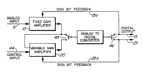
In figure 3, a fixed gain amplifier 10 is
representative of all but the analog to digital converter 13 in
figure 2. The analog to digital converter 13 in figure 3 is
alternately connected to receive first and second analog signals
~ ,~7~ ~3~
from the fixed gain amplifier 10 and a variable gain amplifier
20, via a switch 45. An output of the converter circuit 13 is
coupled by a switch 46 to provide digital outputs alternately on
leads 15 and 25.
The converter 13 is operated in this example at a 16
Khz sampling rate, in synchronism with the switches 45 and 46.
Signals from the output of the fixed gain amplifier 10 are
inversely amplified in the variable gain amplifier 20 in
accordance with a gain factor controlled via a control input 44.
Both the amplifiers 10 and 20 are mid-operating point stabilized
in response to sign bits coupled via respective paths 15a and
25a. Hence the sign bits on the path 15a are the inverse of the
sign bits on the path 25a. In an another example, not shown,
the switches 45 and 46 are not used and only the output of the
variable gain amplifier is converted to a digital signal. In
this example, the path 15a is connected directly to the path 25a
but differs therefrom in that it includes an invertor in series
therewith for inverting the sign bits on the path 25a for use in
stabilizing the amplifier lo.
In figure 4, the variable encoder circuit illustrated
includes all the elements of the prior art figure 2 (which are
correspondingly labeled) in addition to elements which provide
an example of the variable gain amplifier 20 in figure 3. With
exception of the capacitor 12 and a capacitor 22, all of the
elements in figure 4, are preferably integrated in CMOS
transistor technology within an integrated circuit. In this
example, low pass filters 17 and 27 are implemented ~y switched
capacitor resistances. An operational amplifier 21 includes a
~7~
non-inverting input which is used as a stabilizing node for mid-
point operating bias potential. The bias potential is generated
by the capacitor 22 and the switched capacitor resistance 27 in
response to sign bits from a latch 26 which captures and holds
sign bits from the digital output 25, at an 8 KHz sampling rate.
A resistance element 40 is connected via a lead 41 to the output
of the low pass filter 14 and via a lead 42 to an output of the
amplifier 21. An inverting input of the amplifier 21 is
capacitively connected to its output via a capacitor (of about
5pf) 23 and is also connected to the resistance element 40 by a
variable tap 43. The tap is alterable by a control input shown
at 44.
The output mid-point of the amplifier 11 is directly
coupled through the filter 14 such that a potential difference
between the output of the amplifier 11 and the amplifier 21
appears across the resistance element 40. The variable tap 43,
when adjusted, travels through a d.c. potential difference which
counter balances the d.c. output of the amplifier 20 such that
it remains at about the preferred mid-point even during those
periods shorter than the time constant of the integrating
function of the elements 22 and 27.
An example of the resistance element 40 is illustrated
in more detail in figure 5. This example is particularly
adapted to being integrated in the CMOS technology. Thirty-two
columns labeled CO-C31 each include ten field effect transistors
being arranged in a series string and terminating at a rail
which corresponds to the variable tap 43. Thirty-two
corresponding resistance segments, labelled Rl-R32, are
~;~71~3~
connected in series between the leads 41 and 42. The first
column CO is connected to a junction of the lead 41 and the
resistance segment Rl, and the second column Cl is connected to
a junction between resistance segments Rl and R2 and so on as
illustrated.
The control input 43 includes five leads labelled A-E,
each of which is connected to gate electrodes, as exemplified at
55, of a pair of the field effect transistor ~FET) in each of
the columns and which are of opposite conductivity type. For
convenience, this is illustrated by one of the pair having a
gate electrode with an inversion symbol 55' attached.
For example, in column CO a FET 52 is paired with a
FET 53 which includes the inversion symbol. Both the FETs 52
and 53 include gate electrodes which are connected to the lead
43A but the FETs 52 and 53 respond oppositely to a control
signal on the lead so that when one FET is OFF, the other is ON.
For simplicity of illustration, the control leads are shown as
running straight across each respective row. This is intended
to indicate that the gate electrode of each of the FETs is
connected to its respective control lead. It will be noticed
that in each column, half of the FETs are each bridged by a
conductive path, as exemplified at 54. The conductive paths or
bridges are organized in a prearranged pattern such that only
one of the columns CO-C31 will be switched ON in the presence of
any five bit binary word applied at control input 44. More
particularly in this pattern, one of each FET pair is bridged
while the other is not, such that the bridged FET is of no
function. Therefore, each of the leads A-E is of effect with
~ 7~ 5~
respect to only one FET in each row even though it is connected
to its respective pair of FETs in each row. This particular
structure was arrived at as a matter of convenience in
fabricating the example embodiment in the MOS technology.
In this particular example of the encoder in figure 4,
the resistance element is so arranged to provide a gain
alteration of 1.7 decibel steps through a range of 52.7
decibels.