Note: Descriptions are shown in the official language in which they were submitted.
CHP/M-423
~2~3~i
1 SUPPORT ASS~MBLY FOR INTEGRATED CIRCUITS
2 V. K~ Sahakian
3 Jon Long
ACKGROUND OF THE INVENTION
6 Field of the Invention
7 This invention relates to an integrated circuit package
8 and in particular to a support assembly for integrated
g circuit chips.
1~
11 Description of the Prior Art
1~ Integrated circuits (IC) generally comprise a number of
13 gates or flip-flops that are packaged in a single IC
14 container. The IC package provides input and output pins,
pads, or leads which are connected to plated strips on
16 circuit boards or other means to form a complete circuit of
17 which the IC is a part. The IC chips are packaged by die
1~ attachment to paddles of lead frames. The lead frames are
19 either stamped or etched according to the quantity to be
made. In the event that a large quantity is to be produced,
21 then stamping techniques are employed. On the other hand,
22 if only a small quantity of frames are needed, then they may
2 be made by slower photolithography and etching techniques.
24 The etching techniques allow finer tolerances than the
stamping method. After die attachment, the bond pads of the
26 device are connected to the leads of the lead f rame by means
~7 of a fine metallic wire. Upon completion of the chip to
2B frame interconnection, the chip and interconnections are
2g encompassed by the IC package.
33 One problem that is encountered with stamped frames is
31 the limitation of the space between the leads and components
3 of the IC assembly imposed by the thickness of the metallic
frame. The acceptable space between leads is approximately
l.S times the thickness of the metal, which generally is a
copper sheet of about .008 inches thick, for example.
Therefore, the spacing between leads that is required is at
least .012 inches. If 25 leads, by way of example, are to
37 be provided, then a total spacin~ of .300 inches i5
^~
p~
-- 1 --
CHP/M-423
~2~3~
l needed. This spacing creates too large a distance between
2 the IC device, which is located centrally on the frame, and
3 the leads at the periphery of the frame. Therefore a lower
4 yield in production is obtained due to excessive length of
the interconnecting wires. Also, the extra length required
6 does not allow for a compact assembly with dimensions that
7 are required by IC technology. The problem is compounded
when the number of leads is increased thus necessitating a
g significant increase in space of the IC and the frame leads.
1~ On the other hand, if a relatively thin tape-like
~1 support is used, such as an .001 inch thick metallic sheet,
~2 the spacing re~uirement is substantially reduced so that the
13 leads can be located close to the IC device. However, such
~4 thin metal tapes of this type are too flexible and are not
rigid enough for assembly.
16
SUMMARY OF TEIE INVENTION
17
18 An object of this invention is to provide an improved
19 support assembly (lead frame) for integrated circuit chips.
Another object of the invention is to provide a com-
21 posite IC support which provides a needed rigidi~y, and
22 realixes proper alignment of the IC device and conductive
leads.
Another object is to provide a support assembly for an
IC package that achieves high density of the conductive bond
26 locations of the IC device and a high pin count.
27 According to this invention, an IC package includes a
composite support assembly formed with a rigid lead frame
and a thin flexible tape-like structure. The tape-like
structure is configured, preferably by etching, with inner
bonding fingers, and with outer lead fingers that connect to
the inner lead ingers. The lead fingers on the tape-like
structure are disposed in a short pitch, high density
pattern that can be formed as a result of the very thin
structure of the flexible tape material. The lead frame is
formed with leads that connect to the outer lead fingers of
36 the tape-like structure and external circuitry. The
37 composite support assembly allows the wire lengths
38
2 --
CHP/M-423
~723~
l connecting the IC chip to be shortened. As a result, the
2 support assembly can be made with a greater number of leads
3 and a higher pin count employing a standard size frame.
~ Fine line definition of the high density lead fingers is
realized with resultant improved accuracy and proper
6 alignment of the tape-like structure on the lead frame.
BRIEF DESCRIPTION OF THÆ DRAWINGS
g The invention will be described in greater detail with
reference to the drawings in which:
1} Fig. l is a top plan Yiew of a support assembly for an
12 IC chip, made in accordance with this invention;
13 Fig. 2 is an enlarged sectional view of a portion of
1~ the assembly of Fig. l including the IC chip and package;
l~ Fig. 3 is a side sectisnal ~iew of a support assembly
16 for an IC chip incorporating the flexible tape-like struc-
17 ture and rigid lead frame assembly of this invention with
1~ the IC chip and package; and
19 Figs. 4A-4H illustrate the process steps of assembling
the composite IC assembly.
21 Similar numerals refer to similar elements throughout
22 the drawings.
23
24 DESCRIPTION OF THE PREFERRED EMBODIMENT
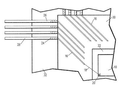
With reference to Fig. l, a composite support assembly
26 (lead frame) for an IC chip includes a flexible tape-like
structure 14 that is joined to a rigid lead frame 12. The
tape-like structure, which is preferably made of a thin
copper sheet of about .001 inches in thickness and a
dielectric film of about .003 inches in thickness, is
configured by well known photolithography and etching
processes. The lead frame is preferably made as an
integral piece that has been mass produced by stamping. The
lead frame is formed from a rigid copper plate, about .008
inches in thickness.
As illustrated in Figs~ 2 and 3, the thin tape-like
3~ structure 14 is configured with inner lead fingers 1~ that
37 are electrically connected by bond wires 18 to bond pads 20
38
-- 3
C~P/M- 4 2 3
1 formed on an exposed surface of the IC chip 10. The
2 ~pposing surface of the IC chip is attached to tape-like
3 s~ructure 14 through a die attach pad 22. Th~ tape-like
~ structure 14 is formed with outer lead fingers 24 that
extend from the inner lead fingers 16 to make contact with
6 coupling lead bonds 26~ thereby providing a continuous
7 conductive path from the i~tegrated circuit to external
8 package leads 28. The assembly including the structure 14
g and frame 12 are housed in a package or module 32. As a
result of the constricted geometry and the necessity for
11 closely spaced patterned elements, including the lead
12 fingers, ~anufacture of an IC package 32 with a relatively
13 large number of lead fingers would be extremely difficult
14 when employing conventional IC packaged designs. The use of
a thin tape-like structure to enable the shaping of the
16 closely spaced lead fingers with fine definition, in
17 combination with the lead frame 12 to provide rigidity,
18 overcomes the difficulties encountered in the prior art.
19 Etching o a thin structure to obtain a desired pattern
affords finer tolerances and better line delineation, which
21 allows a short pitch, high density arran~ement of the etched
2~ elements, including the conductive lead fingers.
23 During production, the flexible tape-like structure 12
24 and the rigid lead frame 14 are positioned in a bonder
apparatus comprising a stripper 34, a thermode 36 and a
26 punch 38 (Figs. 4Ap 4B~. The outer lead fingers 24 of the
27 tape-like structure are aligned with respective coupling
28 lead bonds 26. The punch separates a tape unit 12A from the
tape strip, and the tape unit is moved into contact with the
frame 14 (Fig. 4C). The tape unit is welded t~ the frame by
the application of heat fro~ the thermode, i.e. thermo-
compression bonding or eutectic bonding. The thermode and
the punch are then returned to the home position, and the
assembly of the lead frame with the tape unit is advanced,
enabling repetition of the assembly process (Fig. 4E).
~~ An IC device 10 is then mounted on the composite frame
and tape unit assembly 40 (Fig. 4F), and the IC device is
37 wire bonded to the composite rame ~Fig. 4G). Finally, the
3~
-- 4 --
CHP/M-423
~2~
1 assembly of the bonded devise and the frame 14 is encap~
2 sulated to form an IC package 32 (Fig. 4E~.
3 The composite IC support assembly allows a high pin
4 count with accurate definition of the connecting lead
5 fingers. By virtue of the design of the assembly disclosed
herein, production yield is significantly increased and
7 manufacturing costs are reduced. Since the outer and inner
lead fingers can be brought closer to the IC chip, the bond
g wires between the chip and the inner lead fingers are
shortened. AS a result, a relatively high number of leads
11 can be incorporated in an IC package design. In successful
12 implementations, packages having 68 leads and 132 leads were
13 made employing a standard package mold. The support
14 assembly design vir~ually eliminates losses of IC assemblies
and production resulting from high temperature processing by
16 mechanical orces, such as experienced in previous
approaches to manufacture IC packages. It will be apparent
18 to one skilled in the art that it is not necessary to employ
19 the materials and thicknesses of the frame and tape-like
structure given as examples herein. It is understood that
21 various modifications may be made without departing rom the
22 spirit and scope of the instant invention.
23
24
26
27
2~
~9
31
32
33
34
36
37
38
-- 5 --