Note: Descriptions are shown in the official language in which they were submitted.
27~S7
PHN 11813 l 5.12.1986
Supply circuit for supplying a smoothed direct current to a load
impedance.
The invention relates to a supply circuit for supplying
a smoothed direct current to a load impedance, comprising:
- input terminals for receiving a voltage consisting of a ~irect voltage
component and a periodic alternating voltage component superposed
thereon having a specified ripple period,
- output terminals for connecting the load impedance,
- a series element controllable v a a control input and having a main
current path connected in series with the load impedance,
- a low pass filter having an output on which there is a voltage whose
direct voltage component is determined by at least one filter
capacitor,
- and a differential amplifier having output connected to the control
input of the series element, having a first input to which is supplied
a voltage proportional to the voltage across the load impedance, and5 having a second input connected to the output of the low pass filter.
Such a supply circuit is known from "Patent Abstracts of
Japan", publication Nr. 59-170915, publication date 27-9-1984,
application Nr. 58-44942, date of application 18-3-1983.
The supply circuit described in the aforesaid
publication comprises a differential amplifier whose output is connected
to the base of a bipolar transistor which ~orms the series element. A
first input of this differential amplifier is connected ta the tapping
point of a vo].tage divider connected between the output terminals of the
supply circuit, and the second input of this differential amplifier is
connected to the tapping point of a further voltage divider connected
between the input terminals of the supply circuit. Arranged in parallel
with a resistance of this further voltage divider there is a capacitance,
through which an alternating voltage component of the input voltage is
short circuited. Thus the input voltage divider together with this
capacitance forms a low pass filter. Because of this low pass filter
the alternating voltage component has no effect on the output voltage of
the differential amplifier, thus on the base voltage of the bipolar
.~s; 72~ 7
P~N 11813 2 5.12.19~6
transistor. In order to achieve that there is no alternating voltage
component across the load impedance, the entire alternating voltage
component has to apply across the series transistor. For this to be
achieved the direct voltage between the collector and the emitter of
this series transistor should necessarily be selected equal to at least
the peak-to-peak value of the alternating voltage component. This can
be achieved by selecting the right resistance values of the two voltage
dividers.
This arrangement results in a considerable power
;10 dissipation occurring in the series transistor, irrespective of the real
amplitude of the alternating voltage component. Consequently, this
series transistor continuously operates at a high working temperature
:leading to fast ageing and a short life of this transistor. This is
especially a drawback for systems where high demands are made on the
operational reliability, such as for example telecommunication exchanges.
The invention has for its object to provide a supply
circuit of the type mentioned in the preamble wherein the dissipation of
the series element is electronically adapted to the actual peak of
the alternating voltage component.
To this end the supply circuit in accordance with the
invention is characterized in that the supply circuit further
comprlses:
- discharge means for discharging the current from the filter capacitor
during at least part of the ripple period,
- supply means for providing supply current to the filter capacitor,
which supply current is large with respect to the discharge current,
- a threshold voltage circuit for producing a threshold voltage,
- and a comparator to be supplied with the threshold voltage, having an
input to which the voltage over the series element is applied and
having an output connected to the supply means, for making the
supply current flow if the voltage across the series element is
smaller than the threshold voltage.
The voltage across the series element will generally
consist of a direct voltage component and an alternating voltage
component. As long as the voltage across the series element exceeds
the threshold voltage a large supply current will flow to the filter
capacitor, causing the voltage across this capacitor to reach its
~2~7~
PHN 11~13 3 5.12.1986
mean final value (at a steady state of the voltage across the series
element). This f.inal value is achieved when the charge supplied to the
filter capacitor is equal to the discharge averaged over the ripple
period. As the supply current i.s large relative to the discharge
; 5 current, current will be supplied for only a very short time, i.e., the
current supply-time will be much shorter than the ripple period. As the
voltaye across the series element is smaller than the threshold voltage
for only very short time intervals, the voltage across the series
element during these time intervals will only be slightly lower than the
threshold voltage. By selecting very low value for this threshold
voltage, the total voltage across the series element will be confined to
the sum of this threshold voltage and the peak-to-peak value of the
actuel alternating voltage component, thus avoiding unnecessary
dissipation.
A preferred embodiment of the supply circuit in
` accordance with the invention is characteri~ed in that the series
element is formed by a field effect transistor. By this measure it is
achieved that driving the series element does not require any current,
a low resistance between drain and source of this series element
being possible; for example a 0.2 Q drain-source resistance is possible
at a 2.5 Amp. current, the minimum drain source voltage thus being
approximately 0.5 V.
Further preferred embodiments of the supply circuit in
accordance with the invention are described in the remaining subclaims~
The invention and its advantages are described with
reference to the following figures, with equal reference numerals
indicating the same elements and in which :
Figure 1 sho-~s an embodiment of a supply circuit in
accordance with the invention;
Figure 2 shows the course of several currents and
voltages in dependency of time in the supply circuit in accordance with
the invention.
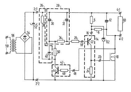
Figure 1 shows a supply circuit whose input terminals 2-1
and 2-2 are connected to a voltage consisting of a direct voltage
component and a periodic alternating voltage component superposed
thereon. A load impedance 60 is connected between its output terminals
4-1 and 4-2. Input terminal 2-1 has a direct connection to output
~72~7~i~
PHN 11813 4 5,12.1986
terminal 4-1, input terminal 2-2 being connected to output terminal 4-2
through a series element 10 designed in the form of a fleld effect
transistor (FET). An output capacitor 12 and a voltage divj.der
comprising two resistors 6 and 8 are connected in parallel with load
impedance 60. ~etween the tapping point of this voltage divider and the
input terminal 2-2 a differential amplifier 14 is connected. This
differential amplifier comprises a first input 16 connected to the
tapping point of the aforesaid voltage divider, a second input 18 and an
output 20 connected to the control input of transistor 10. Differential
amplifier 14 comprises a transistor 22 whose emitter is connected to
input 16 and whose base is connected to input 18 and a collector
resistor 2q on the one hand connected to the collector of transistor 22
and on the other to the input terminal 2-2; the collector of transistor
22 being connected to output 20.
The supply circuit further comprises a low pass filter 28
whose output is connected to input 18 of the differen~ial amplifier 14
vla a resistor 26. This low pass filter consists of two capacitors
30 and 32 each being connected on one side to iDpUt terminal 2-1; the
other sides of these capacitors are interconnected vla a resistor
34. The junction point of capacitor 32 and resistor 34 forms the
output of the low pass filter 28; the input of this filter is formed by
the ~unction point of capacitor 30 and resistor 34. The values of the
components of this low circuit pass filter are chosen such that the
cutoff frequency of this filter is much lower than the ripple frequency
of the alternating voltage component.
The supply circuit also ~omprises supply means 36,
consisting of a series arrangement of a resistor 38 and a diode 40,
which series arrangement is connected between input terminal 2-1 and the
input of low pass filter 28.
The supply circuit further comprises a comparator 42
likewise designed as a threshold ~oltage circuit. This c~mparator
consists of a transistor 44 and a base resistor 46 connected thereto.
The side of resistor 46 not connected to the transistor forms the
input of comparator 42, the collector of transistor 44 forming the
output of this comparator; the emitter of transistor 44 is connected to
input terminal 2-2. The input of comparator 42 is connected to output
terminal 4~2, its output being connected to the input of low pass filter
, ., , . ,., ,~ .
"` ~2~7~5~
PHN 11813 5 5.12.1986
28 through a res:istor 50. Resistor 50 has the function of current
discharge means for discharging the current from the filter
capacitor. The output of comparator 42 is likewise connected to the
junction point of resistor 38 and diode 40.
The input voltage of the supply circuit is received from
the energy network vla the mains connection 58. This mains connection
forms the primary side of a transformer 56, whose secondary side is
connected to a rectifier bridge 54. To the output of this rectifier
bridge and also to the input terminals 2-1 and 2-2 a supply capacitor 52
is connected for smoothing the pulsing direct voltage supplied by the
rectifier bridge 54.
After the mains voltage is switched on vla transformer 56
supply capacitor 52 will be charged. Via load resistor 60 and base
resistor 46 transistor 44 is rendered conductive. Conse~uently, the
filter capacitors 30 and 32 are charged vla resistor 50 so that
transistor 22 is rendered conductive. This causes transistor 10 to
receive a positive gate-source voltage and to be rendered conductive,
~ thus decreasing the voltage across transistor 10. This process
`~ carries on until the voltage across transistor 10 has come near the
` 20 threshold voltage of comparator 42. This threshold voltage ~s formed by
the diodeforward voltage of the base-emitter diode of transistor 44.
At this voltage across transistor 10 the supply circuit in accordance
with the invention assumes the steady state, as will be further
explained with reference to Figure 2.
The top graph of Figure 2 shows the course of the supply
current I1 to filter 28 and the discharge current I2 from filter
28. Supply current I1 is applied to the filter vla resistance 38 and
diode 40, discharge current I2 from the filter being discharged vla
resistor 50.
The bottom graph of Figure 2 shows the course of the
voltage VD on the drain of transistor 10, and the threshold voltage
VTR of comparator 42. The ripple period is indicated by T, the
current supply interval bein~ indicated by t1, the curren~ discharge
interval being indicated by t2.
If the drain voltage VD of transistor 10 exceeds the
threshold voltage of comparator 42, transistor 44 will be in the
saturated state. Consequently, the collector voltage of transistor 44
.. :.: .
- 1 2 7 ~ 7 S ~
PHN 11813 6 5.12.19~6
will substantially be equal to the voltage of input terminal 2-2. Diode
90 will be rendered non-conductive as a result of which the supply
current I1 will be equal to æero. There is a discharge current I2
running through resistox S0 as represented in Figure 2. The value of
this discharge current is determined by the voltage on the capacitors 30
and 32 and the resistance of resistor 50. The voltage on the aforesaid
capacitors is substantially equal to the sum of the tapping point
voltage of the voltage divider formed by the resistors 6 and 8
and the diode forward voltage of transistor 22. The voltage level
across these capacitors is thus determined by the dividinq ratio of
resistance 6 to resistance 8.
The circuit further comprises a zener diode 62 inserted
between the emitter of transistor 22 and the input terminal 2-2. When
switching on the mains voltage the collector-emitter voltage could
become too large, though in addition, this zener diode likewise limits
the gate voltage of transistor 10, which must not exceed for example 20
V.
The moment when the drain voltage of transistor 10
becomes lower than the threshold voltage of comparator 42, transistor 44
will be rendered non-conductive. Consequently, a supply voltage can
flow through resistor 38 and diode ~0 to the capacitors 30 and 32 of
low pass filter 28. This supply current will flow until the drain
voltag~ of transistor 10 exceeds the threshold voltage of comparator 42
again. Resistor 3~ will now be selected to be much smaller (for
example a factor lG) than resistor 50, so that the supply current I1
is much larger than the discharge current I2.
When the supply circuit is in the steady state the charge
~supplied to the filter capacitors averaged over the ripple period T,
has to be as large as the discharge from the filter capacitors. If
the supply current I1 exceeds the discharge current I2 by far the
supply interval tl will thus be much smaller than the drain interval
t2. The latter situation can only appear if the negative peaXs of the
drain voltage VD of transistor 10 fall only slightly below the
threshold voltage VTR. Thus it is achieved that in the steady
state the voltage acxoss transistor 10 never exceeds the sum of the
threshold voltage and the peak to-peak value of the ripple voltage,
thus avoiding unneccessary dissipation.
7S7
PHN 11813 7 5.12.1986
A practical embodiment of the supply circuit in
accordance with the invention comprises components as stated in the
followillg table:
reference gumeral ~YE~ of comPonent value or tv~e
6 resistor 10 kQ
8 resistor 2,7 kQ
field effect transistor Philips BUZ 31
12 capacitor 22 ~F
22 PNP-transistorPhilips 2N 2907
1024 resistor 100 kQ
26 resistor 2,7 kQ
capacitor 22 ~F
32 capacitor 22 ~F
34 resistor 2,7 kQ
1538 resistor 10 kQ
diode Philips BAV 10
: 44 NPN-transistorPhilips BSX 20
46 resistor 1 kQ
resistor 100 kQ
2052 capacitor 10 mF
62 zener-diode Philips BZX 79