Note: Descriptions are shown in the official language in which they were submitted.
~7~
BACKG~O~D OF THE I~ENTION
This invention relates to a semiconductor device
of overvoltage self-protection type which can be safely
.voltage-triggered when an overvoltage exceeding its
breakdown.voltage is applied thereto.
,~hen an overvoltage exceeding a breakdown
voltage is applied to a ~hyristor, the thyristor tends
to be destroyed due to the flow of a breakdown current.
For the purpose of protecting the thyristor against the
overvoltage, a protecting circuit has been additionally
provided, resulting in an increased cost and an increased
number o~ parts of the device. From the aspects of reduc-
tion of the cost and improvement in the reliability
owing to a decrease in the number of parts of the device,
it has been strongly demanded that the thyristor possesses
the function of protecting itself against an overvoltage.
A t~ristor having.such a protective function is called
a thyristor of overvoltage self-protection type. Fig. 1
shows Va~ious kinds of prior art thyristors of overvoltage
sel~-pxotection type.
A prior art thyristor of overvoltage self-
pro.tection type disclosed in Japanese Patent Unexamined
PublicatLon.No. 52-125181 has a structure as shown in
Fig. lA. Referring to Fig. lA, a semiconductor substrate.
1 includes a p-type emitter layer 2, an n-type base layer
- . , ' ' . -
' ' : .,', ' ' '~.' ~ . '
,.. : ,:' ',, '
- , " ~, ., : , , ,
. , ..... . : :- .
~2~
1 3, a p-type base layer 4 and an n-type emitter layer 5.
.~n anode 6 and a cathode 7 make low ohmic contact with
the p-tyoe emitter layer 2 and n-type emitter layer 5
r~spectively~ and an etched region 8 extending into the
p-type base layer 4 is provided on the cathode side.
The term "~tched region" is used herein to denote a
region formed by removing a semiconductor member as by
etching~ ~lthough the semiconductor member may be
re~oved by sand blasting or grinding, removal by etching
is predominant for improving the dimensional accuracy.
~hererore, such a re~ion is generally defined as an etched
re~ion. In the present invention too, the term "etched
region" is used according to the prior art naming. A
gate electrode 9 makes low ohmic contact with the p-type
1~ base layer 4 around the etched region 8. The p-type base
layer 4 penetrates the n-type emitter layer 5 at spaced
positions to make low ohmic contact with the cathode 7
to provide a so-called shorted emitter structure.
In such a thyristor, the depth of the etched
re~ion 8 determines an overvoltage, that is, a self-
protection overvoltage against ~hich the thyristor is
to be protected. More particularly, the position of the
bottom surface of the etched region 8 is such that it
does not cut a central junction Jc formed between the
n-type base layer 3 and the p-type base layer 4 and
is located in a depletion layer that is produced 1n the
p-type base la~er 4 when the central junction Jc is
xeverse biased to bear the voltage withstand function
: ::
~- 2 -
, - . . ' '
-
. , .:
' . ., . , ' , ' . , ', '
' ~ ' , :
~L2~
1 thereby placing the thyristor in a reverse blockin~ state.The function of the etched regic,n 8 is to increase the
electric field intensity in the depletion layer between
the bottom surface of the etched region 8 and the central
junction Jc, so that, when a predetermined self-protected
switching voltage is reached, breakover occurs in the
portion where the field intensity is high, thereby
attaining the required self~protection. However, the
thyristor structure shown in Fig. lA is not satisfactory
in that the self~protected switching voltage fluctuates
greatly depending on the flatness of the bottom surface
of the etched region 8.
Another prior art thyristor of overvoltage
self-protection type disclosed in Japanese Patent Unexamin-
ed Publication No. 53-80981 has a structure as shown
in Fig. lB. Referring to Fig. lB in which the same
reference numerals are used to designate the same or
equivalent parts appearing in Fig. lA, the p-type base
layer ~ is formed after formation of the etched region 8.
Still another prior art thyristor of overvoltage
self-protection type disclosed in Japanese Patent Unex~
amined Publication No. 59~-158560 has a structure as shown
in Fig. lC. Refexring to Fig. lC in which the same
reference numerals are used to designate the same or
~5 equivalent parts appearing in Fig~ lA, the p-type layer 4
is formed, and, then, the etched region 8 is so formed
as to extend to the central junction Jc. Subsequently,
the acceptor ls diffused again into the area which
-- 3
- : ~ . -. . - . ., :. .,
- . . : . .
-; ' -,
1 includes the e-tched region 8, thereb~ providing a curved
( portion in the central junction Jc.
In each of the thyrlstor structures shown in
Figs. lB and lC, the curved portion is formed in the
5 central junction Jc immediately beneath the etched
region g, so that the electric field intensity in the
depletion layer can be increased at the curved portion,
thexeby exhibiting the effect of self-protection.
However, in the thyristor structures shown
in Figs. lB and lC, the self-protected switching voltage
varies greatly depending on the configuration and radius
of curvature of the etched region 8. Therefore, it is
necessary to accurately control the configuration of the
etched region 8. However, it has been very difficult to
highly accurately control the configuration of the etched
region 8 according to the prior art techni~ue of wet
etching or the like.
SU~h~Ry OF THE ~NVENTION
It is a primary object of the present invention
~0 to provide a semiconductor device of overvoltage self-
protection type whose self-protected ~witching voltage
can be accurately controlled.
The semiconductor device according to the
present invention is featured by the fact that, at side
wall portions of an etched region provided in a p-type
base layer forming a central junction Jc bearing the voltage
withstand function, the electric field intensity of a
-- 4
- ., :
.
- . - - - ;
- :. ' `: ' -
.
. . ' ' ' :
~7~
depletion layer extending toward a cathode is increased by
an amount corresponding to the volume of the depletion
layer lost by the provision of the etched region, so that
breakover occurs at the side wall portions thereby
exhibiting the effect of self-protection.
More specifically, the invention consists of a
semiconductor device of overvoltage self-protection type
comprising: a semiconductor substrate having a pair of
major surfaces, said substrate including an anode emitter
1~ layer of firs~ conductivity type, a first base layer of
second conductivity type, a second base layer of first
conductivity type, and a cathode emitter layer of second
conductivity type, said layers adjoining each other between
the major surfaces; a pair of main electrodes making low
lS ohmic contact with the outermost layers of said semi-
conductor substrate respectively; and an etched region
formed in said second base layer and said cathode emitter
layer, said first and second base layers forming a pn
junction bearing a reverse voltage applied across said
` ~ main electrodes, said etched region extending from one of
the major surfaces without cutting said pn junction, said
cathode emitter layer and said second base layer adjoining
each other in a plane parallel to said one major surface,
the cathode emitter layer being exposed at side walls of
the etched regionj and the bottom surface of said etched
region being located at a position deeper than a depletion
layer produced in said second base layer as a result of
application of the reverse voltagel the intensity of an
.,
.
~ '
electric field established in said depletion layer being
increased by an amount corresponding to the volume of said
depletion layer lost by the provision of said etched
region whereby breakover occurs at side wall portions of
said etched region.
BRIEF DESCRIPTION OF THE DRAWINGS
Figs. lA to lC are schematic sectional views
of part Q~ semiconductor substrates of prior art thyristors
of overvoltage self-protection type respectively.
Fig. 2 is a schematic sectional view of part of
a semiconductor substrate of an embodiment of the thyristor
of overvoltage self-protection type according to the present
invention.
Figs. 3A and 3B illustrate the principles o
lS the present invention.
Fig. 4 is a graph showing the relation between
the diameter D of the etched region and the self-protected
Switching voltage in the thyristor of the present invention.
Fig. 5 is a graph showing the relation between
the ~emperature o~ the junction in the semiconductor
substrate and the self-protected switching voltage in the
thyristor of the present invention.
Fig; 6 is a graph showing the relation between
the value D d of the etched region and the self-protective
25` voltage in the thyristor of the present invention.
Figs. 7~ to 7C show the process for manufacturing
the thyristor of the present invention.
-5a-
- :' -. .
'
: .
. , .: .
: ': , .
` ~. ' `' , ' ~ ' '
.
'
~72~
1 Figs. 8A and 8B show applications of the present
invention to a light-triygered thyristor, in which Fig. 8A
is a schematic plan view when viewed from the cathode
side, and Fig. 8s is a schematic sectional view taken
5 along the line VIIIB - VIIIB in Fiy. 8A.
Figs. 9A and 9B show improved another embodiments
of the thyristor according to the present invention,
in which Fig. 9A is a schematic partial plan view when
viewed from the cathode side, and Fig. 9B is a schematic
sectional view taken along the line IXB - IXB in Fig. 9A.
Figs. lOA and 1 0B show improved another embodi-
ments of the light-triygered thyristor according to the
present invention, in which Fig. lOA is a schematic
partial plan view when viewed from the cathode side, and
Fig. 10B is a schematic sectional view taken along the
line XB - XB in Fig. lOA.
Figs. llA and 11B show improved still another
embodiments of the light-triggered thyristor according to
the present invention, in which Fig. llA is a schematic
partial plan view when viewed from the cathode side, and
Fig. llB is a schematic sectional view taken along the
line XIB - XIB in Fig. llA.
DESCRIPTION OF THE PREPERRED EMBODIMENTS
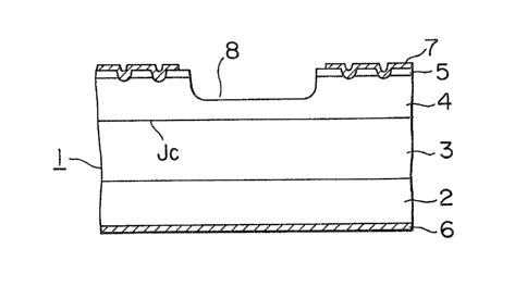
Fig. 2 shows an embodlment o~ the thyristor
according to the present invention. In Fig. 2, the same
xeference numerals are used to designate the same or
equivalent parts appearing in Fig. lA.
- 6 -
:
.- . . . : , , . .:
, . . . :
.: : , ', , '
- ~: . .. . . .
~2~72~
1 Th~ etched region ~ shown in Fi~J. 2 is anoloyous
to the etched region 8 shown in Fig. lA, but differs from
the latter in that breakover occurs at side wall portions
o~ the etched region 8. This feature will be described in
detail with reference to Fig~ 3.
The semiconductor substrate 1 shown in Fig. 3A
has an impurity concentration gradient as shown in Fig. 3B.
When a voltage, which is positive relative to
the potential at the cathode 7, is applied to the anode 6,
the central junction Jc is reverse biased to bear the
voltage withstand function thereby placing the thyristor
in a forward blocking state. The dotted lines indicate
the boundaries of a depletion layer formed in the n-type
base layer 3 and p-type base layer 4. Since the etched
region 8 is provided in the p-type base layer 4, the
depletion layer cannot spread into the p-type base layer
~ at the area where the etched region 8 is present.
Therefore, the depletion layer rises toward the cathode 7
at the side wall portions of the etched region 8 by the
~0 ~uantity of charges QH corresponding to the quantity of
space charges QR of the depletion layer which should
spread in the absence of the etched region 8. However,
the rate of spread of the depletion layer is very small,
since the p-type base layer 4 is formed by impurity
diffusion like the p-type emitter layer 2, and the impurity
concentxation of the p-type base layer 4 shows an exponen-
tial incXease toward the cathode 7. Consequently, the
electric field i~tensity increases at the side wall
- 7 -
.:
.. -
- `' '
' ~
1 portions of the etched region 8, and avalanche breakdown
occurs at those side wall portions of the etched region
8. The slructure is such that the quantity of space
char~es QR corresponding to the volume of the depletion
layer lost by the provision of the etched region 8 acts
to intensify the electric field of the depletion layer
at the side wall portions of the etched region 8, thereby
causing breakover at the side wall portions of -the etched
region 8. Therefore, the etched region 8 need not be as
deep as the etched region 8 shown in Fig. lA. Rather, the
etched region 8 is shallow but has a wide area when
viewed from the cathode side. Thus, the volume of the
depletion layer lost by the provision of the etched region
8 is rather enlarged. In this case, Jche electric field
lS in the portion of the depletion layer immediately beneath
the bottom surface of the shallow etched region 8 is not
substantially intensified, and breakover does no~ occur
at this portion.
The shallowness of the etched region 8 is
~0 advantageous in that not only the period of time required
for forming the etched reyion 8 can be shortened, but
also the flattened bottom surface reduces the possibility
of fluctuation of the self-preventive voltage.
Fluctuation of the space volume of the etched
region 8 leads directly to fluctuation of the self~
pxeventive voltage.
Therefore, the etched region 8 must be formed
as accuxate as possible. In the present in~ention r
-- 8 --
.
' .
- , . . :: :
1 especially the etched region 8 is formed by the technique
of dry etching. ~s compared to the prior art wet etching,
the dry etching can be carried out without regard to
the orientation of the lattice planes of the semiconductor
substrate as well as the impurity concentrations of the
semiconductor layers, and the rate of etching is substan-
tially constant. SF6 is preferably employed as a reaction
c3as in the process of dry etching. When SiO2 is used as
a resist film, the etching ratio between Si and SiO2 can
be selected to be more than 100, and as SiO2 film about 1
~m thick suffices for etching as deep as SO to 100 ~m.
In such a case, fluctuation of the flatness of the bottom
surface of the etched region 8 can be reduced to a very
narrow ran~e of ~1 ~m.
Therefore, when the mask used for forming the
etched region 8 by dry etching is accurately configured,
fluctuation of the self-prevented switching voltage can
be minimized.
When a plurality of thyristors of overvoltage
~0 self-prevention type are connected in series in use,
it is especially effective that they have the same or
equivalent self-prevented switching voltage. That is,
when the thyristors have the same or equivalent self-
protected switching voltage, the individual thyristors
can be triggered at suhs~tantial1y the same time in the
event of application of an overvoltage. If the self-
protected s~itching voltages of the individual thyristors
fluctuate greatly from one another, the thyristor having
-- 9 _
: .
.
'~
: ` :
~27~
1 a lowest self-protected switching vol-tage is trigyered
first, and the thyri~tor having a highest self-pro-tected
switching voltage bears the overvoltage of the entire
device and will be destroyed. In this respect, the
present invention is quite effective in that the self-
protected switching voltage can be accurately specified.
The relation between the volume of the etched
region 8 and the self-protected switching voltage of the
thyristor will now be described.
Fig. 4 shows how the self-protected switching
voltage VBo changes when the diameter D and depth d of
the etched region 8 are changed. In Fig. 4, the breakdown
voltage in the absence of the etched region 8 is designated
b~ VO, and the self-protected switching volta~e VBo in the
lS prasence of the etched region 8 is normalized by VO.
Suppose that the depth d of the etched region 8 is fixed.
In such a case, the larger the diameter D, the lower is
the self-protected switching voltage VBo~ The fact that
the self-protected switching voltage VBo changes relative
~0 to the depth d of the etched region is disclosed in
Japanese Patent Unexamined Publication No. 52-126181~
However, it is a new fact which has not been revealed up
to now that the self-protected switching voltage VBo
changes relative to the diameter D of the etched region 8.
Fig. 5 shows the temperature dependence of the
self-protected switching voltage of the thvristor of
overvoltage self-protection type shown in Fig. 2. It will
be seen in Fig. 5 that the tendency of changes in the
-- 10 --
.
- : . : .
.
: ~
~27~
1 temperature dependence of the self-protected switching
voltage is almos-t the same despite changes in the diameter
D of the etched region 8. It will also be seen that the
temperature dependence of the self-protected switching
voltage is satisfactory in that voltage variations in
a temperature range of 25C to 12~C are less than 10%.
E~periments were also conducted by changing various
factors including the depth d, resistivity and thickness
of the n-type base layer 3, and thickness of the p-type
base layer 4. The results of the experiments proved that
the characteristics are similar to those shown in Figs. 4
and 5.
Fig. 6 summarizes the relation between D- ~ ) and
the self-protected switching voltage VBo of the thyristor
on the basis of the experimental results shown in Fig. 4,
where D and dl are the diameter and depth respectively
of the etched region 8, and d2 is the thickness of the
p-type base layer 4 remaining in the etched region 8.
It will be seen in Fig. 6 that, when the relation between
VB and D.(d- ) at various values of the diameter D and
depth d of the etched region 8 is plotted, the curves
show substantially the same correlation. Results of
experiments conducted on several samples having various
strUctures including those referred to in Fig. 4 proved
also that curves representing the relation between VB
d~ 0
and D-(d ) show substantlally the same correlation.
Genexally, the self-protected swltching voltage VBo of
a thyristor of overvoltage self-protection type is
, ~ ,:- . . :
' ` : , , , ~ '': ' . ,
. .
selected to be higher than 80% of the breakdown voltage
V0 of a thyristoe having no self-protection~ However,
in order that the value of VB0/VO is larger than 0.8,
it is required from Fig. 6 that the value of D. ~1 ) is
equal to or smaller than 4.5 mm and preferably eg2al to or
larger than 2 mm. To set ~he value of D. ~1 ) in such a
range, ~he diameter D of the etched region ~, or the depth
dl (d2) can be selected as required.
When the depth of the etched region is shallowed,
and the area of the etched region 8 is wid~ned, the
region, which conducts initially in the event of applica-
tion of an overvoltage, can be widened. That is, it is
t~e peripheral side wall portions of the etched region 8
which undergoes avalanche breakdown in the event of
application of an overvoltage. The larger the area of
; the etched region 8, and the wider the region subjected
to the avalanche breakdown, the initial conducting region
becomes correspondingly wider. Thus, the di/dt capability
and the switching power capability dependent upon the area
of th2 initially conducting region are enhanced.
Figs. 7A, 7B and 7C are schematic sectional
views showing part of the process for manufacturing the
thyristor of overvoltage self protection type according to
the present invention. The manufacturing process will now
be described. After diffusing a p-type impurity from the
two major surfaces of an n-type silicon wafer 1, the
wafer 1 is processed by etching to have a predetermined
thickness, thereby forming a p-type emitter layer 2, an
n-type base layer 3 and a p-type ba5e layer 4 as shown in
- 12
:
~27Z~
1 Fi~. 7A. Then, as shown in Fig. 7~, an n-type emitter
layer 5 is formed by a method of selective diffusion
(or a method of etching down). Af~er forminy all the
junctions to provide a thyris~or structure in the manner
above described, an etched region 8 having a desired
diameter and a desired depth is formed in the predetermined
region havin~ a cathode deposited later thereon, as shown
in Fig. 7C. The method of dry etching described herein-
befo~e is used for the formation of the etched region 8,
so that the etching can be accurately controlled, and the
bottom surface of the etched region 8 can be accurately
flattened~
Then, aluminum is deposited at predetermined
positions on the upper and lower major surfaces of the
silicon wafer 1 to provide an anode, a cathode and a gate.
Then, after processing such as bevelling and surface
stabilization, the silicon wafer is sealed in a ceramic
package to produce a thyristor of overvoltage self-
protection type.
~0 Accordi~g to the manufacturing process described
abo~e., the self-protection function can be provided by
merely forming the etched region 8 in the p-type base
layer 4 after formation of all the pn junotions. There-
fore, the thyristor can be simply and conveniently
~5 manufactured without impairln~ the other chaxacteristics.
Figs. 8A and~8B show applications of the present
inVention to a light-triggered thyristor. Referring to
Figs. 8A and 8B, a semiconductor~ substrate 1 includes a
- 13 -
'. ' ; '~
, ~ ; , - ""': ' '
,
~7~
1 ~type emitter layer 2, an n-type base layer 3, a p-type
base layer 4, and a central liyht-receiving n-type emitter
layer 10, and ~he pn ~unction formed between the light-
receiving n-type emitter layer 10 and the p-type base
layer 4 is short-circuited by an elec~rode 11. An etched
region 8 is provided at the center of the central light-
receiving n-type emitter layer 10. Small circles shown
in part of two electrodes 7 and 12 indicate etched-down
portions acting as emitter short-circuiting means.
Although those small holes are distributed all over
the electrodes 7 and 12, they are partly omitted from the
illustration. In the form shown in Fig. 8, the self-
protective region is disposed at the center of the light
receiving section. Generally, a light-triggered thyristor
is designed so that its trigger sensitivity becomes higher
in the order of a light receiving section, an auxiliary
thyristor section surrounding the light receiving section~
and a main thyristor surrounding the auxiliary thyristor
section~ Therefore, by providing the self-preventive
~0 region at the ce~ter of the light receiving section, the
value of tri~ger current turning on the element in the
event of application of an ove~voltage can be made small.
The etched region 8 may be formed in a substan-
tially annular pattern between the light-receiving n-type
emitter layer 10 and the n-type emitter layer 5. In such a
case, the etched region 8 is partly cut. Therefore, it
is necessary to arrange that the p type base layer 4
underlying the n-type emitter layer 5 and light-receiving
- 14 -
.~
.
- : . . : ' :
. ~
~7~
1 n-t~pe emitter layer 10 is not cut by the depletlon layer.
The self-protective voltage can be specified by
the width D of the annular etched region 8. Also, the
etched region 8 of annular pattern permits fur-ther widening
of the area of the initially conducting region.
It is apparent that, besides the application to
the light-triggered thyristor shown in E~ig. 8, the present
invention is also applicable to an electrically triggered
thyristor having a gate electrode provided on its base
layer, a gate turn-o~f thyristor, a bi-directional
thyristor, a bi-directional transistor and the like. In
the case of the transistor, the p-type emitter layer 2
shown in Fig. 2 is replaced by a layer having a high
impurity concentration and having the same conductivity
type as that of the n-type base layer 3 to constitute a
collector layer together with the n-type base layer 3.
The p-type base layer 4 and the n-type emitter layer 5
fu~ction as a base layer and an emitter layer respectively.
According to the present invention, the etched region is
provided in one of the base layer and the collector layer.
The present invention is also applicable to a
semiconductor device of opposite Gonductivity type in
which the p-type and n-type are inverted.
Figs. 3 and 4 show that, when two kinds of
etched regions having the same depth but different
dia~eters axe formed in the semiconductor substrate 1,
breakover occurs at the etched region having the larger
diameter. On the other hand, when avalanche breakdown
~ 15 -
'~ :
~, . ~ ,
.
: L272~
1 current ~lowing between the bottom surface of the etched
region having the smaller diameter and the cen-tral junc-
tion Jc is noted, the sheet resis-tance of the p-type
base layer 4 is high in this portion, and the avalanche
breakdown current is limited by the transverse resistance
of the p-type base layer 4. Therefore, the etched region
having the smaller diameter acts to suppress the value
of current flowing when breakover occurs at the etched
region having the larger dia~eter, so that the seml-
conductor substrate may not be thermally damaged.
Figs. 9A and 9B show another embodiments of the
thyristor according to the present invention in which
two kinds of etched regions are provided on the basis o~
the above consideration.
lS In Figs. 9A and 9B, the same reference numerals
are used to designate the same or equivalent parts appear-
ing in Fig. 2.
In the embodiment shown in Figs. 9A and 9B, a
second etched region 9 which is in the form of a partly
discontinuous slot having a width D2 surrounds substan-
tially a plurality of first etched regions 8 having a
dia~eter Dl. The etched re~ions 8 and 9 have the same
depth, and there is the relat1on Dl > D2. As seen in
Fig. 9A, a non-etched area exists necessarily between the
cathode 7 and all of the etched regions 8 and 9.
Consequently, the surface potential o~ the area surrounding
the etched regions 8 and 9 is the same as that o the
cathode 7, and the same voltage is applied to all of
- 16 -
.. , . . . :
`,: . : .
.
,
~2~
l the etched regions 8 and 9. As in the case o~ the thyristor
shown in Fig. 2, the depth of the etched reyions 8 and 9
is selected so that the depletion layer spread in the
p-type base layer 4 reaches the etched regions 8 and 9
when a forward overvoltage is applied to the thyristor.
In this case, the breakover voltage VBo can be specified
not only by the depth of the etched regions 8 and 9,
but also by the diameter (or the width) of the etched
regions 8 and 9, as described already with reference to
~Q Figs. 3 and 4. The etched regions 8 and 9 have the same
depth. Therefore, the larger the diameter (or the width)
of the etched regions 8 and 9, the avalanche breakdown
voltage becomes lower, and the breakdown voltage of the
region 8 is lower than that of the region 9. The avalanche
lS breakdown occurs in the region 8 when an overvoltage is
applied to the thyristor. The avalanche current produced
as a result of the avalanche breakdown flows in~o the
cathode 7, but the etched region 9 exists in the path of
this current. The sheet resistance in this region 9
is larger than that of the non-etched area. This sheet
resistance acts as a limiting resistance for the breakdown
current and acts also as a ballast resistance by which
the breakdown current is uniformly distributed to the
cathode 7. Therefore, the second etched region 9 improves
the di/dt capability of the thyristor dur1n~ the self-
protected operation. The value of this limiting resistance
can be chan~ed as desired by changing the width and
number of slots o~ the etched region 9. Since the etched
- 17 -
~L~7~
1 regions 8 and 9 have -the same depth, the same photomask
can be used for the simultaneous formation of these
etched regions.
The thyristor is turned on by merely applying
a gate signal, which is positive relative to the potential
at the cathode 7, to a gate electrode 13 making low ohmic
contact with the p-type base layer 4 exposed to the
cathode-side major surface of the thyristor.
Figs. 10A and 10B show plan pattern and a
vertical section taken along the line III - III in Fig.
10A respectively, when the self-protected s~ructure of
the present invention is applied to a light-triggered
thyristor. In Figs. 10A and 10B, the same reference
numerals`are used to designate the same or equivalent
parts appearing in Figs. 9A and 9B. Referring to Figs.
10A and 10B, a plurality of self-protection regions or
first etched regions 8 are disposed around an n-type
auxiliary emitter layer 20, and a plurality of limiting
rasistance regions or second etched regions 9 having a
width D2 different from the diameter Dl of the first
etched regions 8 are disposed outside of the first etched
xegions 8.
Figs. llA and llB show modifications of the
light-triggered thyristor shown in Fig. 8. Referring to
Fig. 11, a plurality of etched regions 8 are provided in
the n-type emitter layer 5 which forms the auxiliary
thyris~or around the centxal light-receiving emitter
layer 10. Provision of th~ plaral etched regions 8
- 18 -
- . . - , - .: ,: . .
,
- :. :, - ;
. . . . .
: , ' , . ' . . :
:. ' ~ ,- ' ' ' ' : ', '
~2~7~8~
1 widenes the region initially turned on. Also, since the
etched regions 8 are formed in the n-type emitter layer
5, avalanche current produced in the event of application
of an overvoltage acts to effective]y forward~bias the
adjacent pn junction.
It is apparent that the present invention is
effectively applicable to a gate turn-off thyristor and a
bidirectional thyristor besides its application to a
light-triggered thyri.stor and an electric gate thyristor.
1~ It will be understood from the foregoing detailed
description that the presen~ invention provides a semi-
conductor device which can be easily manufactured and yet
whose self-protected switching voltage can be accurately
controlled.
- 19 -
.
. - . ~ ,. , .' .
.
- ~