Note: Descriptions are shown in the official language in which they were submitted.
PHF 85596 1 8.08.198
Exposure arrangement for the production of masks.
The invention relates to an exposure arrangement for the
pxoduction of masks, using a computer-aided design system, which
arrangement comprises :
- a cathode-ray tube which forms an image of the mask on the
S ~creen of the tube, and an optical system which projects the image of
the mask on to a substrate which is to be exposed.
Such an arrangement is used in the manufacture of semi-
conductor devices, in the thin-film and thick-film technique, in
production processes in the photographic industry...
Such an invention is known from JP 58.1~923 which
describes an arrangement consisting of a cathode ray tube having a glass
screen which is provided with a phosphor layer in front of which there
is positioned an array of optical fibres which catches the light rays
issuing from the screen and conducts them in the form of parallel
beams. In this way, a substrate located at one end of the array of
optical fibres is exposed by light issuing from the screen on which
appears the geometrical pattern of the mask produced by means of a
computer-aided design system. Apparently, this device is designed to
provide the most direct way of utilising the mask image as it appears on
2~ the display console of the computer-aided design system.
However, the said arrangement has some disadvantages.
Firstly, the magnification of the system can only be equal to 1,
the dimensions of the projected image being equal to the dimensions of
the image of the screen. Secondly, as the screen of the tube and the
array of optical fibres are made of glass, the spectrum emitted by
the photosensitive layer can only be situated in the visible spectrum.
Consequently, the final definition of the projected image is limited bY
the large wavelength of light. Moreover, as the cathode-ray tube used
is of a standard type, i.e. it is adapted to the human eyesight, it
exhibits a low brightness which is unsuitable for an exposure
arrangement and, consequently, leads to long exposure times and an
increase in reconstruction errors.
- - - :. ....
. .
''
,, ,, '~ "' ', . - '
PHF 85596 2 a.os. 1986
Consequently, it is an object of the invention to enable
exposure of masks and allow for their magnification and reduction.
A further object of the invention is to provide the final projected
image with a spatial definition whi.ch is sufficiently compatible
with the desired applications, whilst considerably reducing the exposure
time~
The invention as described in the opening paragraph is
characterized in that
the cathode-ray tube is a high-brightness tube the screen of which is
1~ provided, firstly, with a phosphor which emits in the ultraviolet
spectrum, and, secondly, with a cooling circuit for the phosphor, and
in that the optical system is designed for use in the ultraviolet
spectrum and operates on the ultraviolet image provided by the screen of
the high-brightness tube~
The present invention makes use of techniques which are
gaining ever more ground and which consist in forming masks for
patterning an electronic circuit by means of a computer. The present
state-of-the-art techniques which do not make direct use of the image
formed on the screen make use of an intermediate mask formed on a solid
carrier. In the present invention this stage is left out.
When the electronic circuit is patterned, an image is
formed on the screen of the display console. The image formed is used
by the user to align the pattern of the circuit. When direct use is
made of the image, there are several drawbacks which have just been
~5 analysed.
When the alignment of the pattern is obtainedl a high-
brightness tube is electrically connected in parallel, in accordance
~ith the inventionl to the display consolel making use of the same
scanning and synchronization signals. The said high-brightness tube,
generally has reduced dimensions, for example 90 x 70 mm. The interior
of the screen of the high-brightness tube is coated with a phosphor
which emits ili the ultraviolet spectrum, for example, between 365 nm and
400 nm.
In comparison with the visible light these shorter wave
lengths enable an increased sharpness of the pattern of the final
image. The image formed on the screen of the high-brightness tube is
transferred by an optical system which is adapted to the ultraviolet
, . .
,
: ,.. : :': .
.
~2~72~L~
PHF 85596 3 8.08.1986
spectrum. Dependent upon the object, the image can be magnified,
xeduced or simply transferred.
In order to facilitate the use of the exposure
arrangement for the successive exposure o~ different masks, reference
marks to facilitate the superposition of successive images are provided
at the periphery of the screen of the high-brightness tube, outside the
effective field. These reference marks consist of small patterns of a
phosphor which emits in the visible spectrum. The optical system is
adapted to transmit the light emitted in the visible spectrum.
The high-brightness tube and the optical system are
jointly fitted in a housing.
In order to carry out the exposure process the image must
be fixed for the time of the exposure, with only small variations in
position. The exposure time can be substantially reduced by using a
high-brightness tube which provides a high light flux.
In accordance with a first preferred alternative
embodiment the persistence of the image on the screen is ensured by
using a storage tube as a high-brightness tube, which comprises a
writing gun, one or more flooding guns, collimation means and a metal
~0 grill coated with an insulator which is locally charged with static
charges~ Thus, it is possible to produce a latent electronic image on
the said grill by means of a writing gun which is subsequently read
using the appropriate flooding guns. Thus, an increased electric power
is obtained and, consequently, a more luminous and better contrasting
-~5 image.
In order to obtain a high brightness without
- image aberrations, the tube produces an electric power
density for the excitation of the phosphor, which may at least be equal
to, substantially, 2 Watt/cm2, the flooding gun producing a uniform
current density lower than 0.025 A/cm in the output plane of the
flooding gun.
In accordance with a second alternative embodiment, a
high-brightness tube is used which does not have a storage capacity. In
this case the image persistence is ensured by recurrently scanning the
image.
Taking into account the dissipated electric power, in
these two alternative embodiments the high-brightness tube comprises a
- . , . - :
-, . . .. .
.
- . . ,
PHF 85596 9 8.08.1986
screen-cooling circuit.
By adapting the UV optical system to specific
applications, magnification, reduction or unity scale imagetransfer
becomes possible. Consequently, it is possible to proauce masks by
exposing photosensitive lacquers deposited on substrates, such as
semiconductor arrangements or others.
The invention will now be explained in more detail by
means of drawings which are given as non-limitative examples and
represent :
Figure 1 : a schematic representation of the exposure
arrangement in accordance with the invention, which is coupled to a
computer-aided design system,
Figure 2 : a sensitivity curve of a phosphor which emits
in the ultraviolet spectrum,
Figure 3 : a drawing of a high-brightness tube which
comprises a storage screen and a phosphor which emits in the
ultraviolet spectrum.
Figure 9 : a representation of the electron trajectories
of a flooding gun.
Figure 5 : a representation of the electron trajectories
of the collimation means.
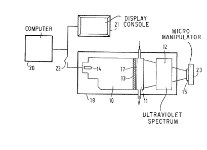
Figure 1 represents a computer-aided design system which
is symbolically represented by a computer 20 and a display console 21 as
used in accordance with the prior art.
The operator carries out the alignment of the pattern in
the usual way. After this, the exposure arrangement in accordance with
the invention is connected in parallel to a display console 21 by means
of a contactor 22. The invention comprises a housing 18 in which are
arranged a high-brightness tube 10 and an optical system for the
ultraviolet spectrum 12. The high-brightness tube lO is provided at the
side of its output with a phosphor 13 which emits ultraviolet
radiation. The said phosphor 13 is excited by electrons issued from an
electron gun 19. The high-brightness tube is designed to operate under
high beam currents, which makes it necessary to cool the screen by means
of a cooling circuit 11 in which a fluid circulates.
The high-brightness tube in accordance with the invention
makes it possible to reduce the exposure times, whilst using UV
. . . : . :
.
. . ~;
%
PHF 85596 5 8.0~.1986
sensitive laquers which are commercially available, for example laquer
no. 1350 marXeted by S~IPLEY (llnited States). On/off operation
obtained by a bistable drive of the Wehnelt electrode of the tube
results in a maximum contrast, which is an advantage of the present
invention. Moreover, it is possible to invert the polarity of the video
signal, which makes it possible to obtain a mask which represents a
positive or a negative image without having to change the type of
laquer. The light beam emanating from the high-brightness tube which is
provided with a cooling circuit, penetrates into a UV optical system 12
which produces an image on a substrate 15 which is positioned relative
to the optical system by a micromanipulator 23.
The optical system must be adapted to the emission curve
of the phosphor. Consequently, for an emission wavelength of 405 nm, it
is possible to use the following objective lenses : S. Planar no. 107739
or no. 107751 marketed by CARL ZEISS (Federal Republic of Germany).
The phosphor may be made of a phosphor P5 as manufactured
by RIEDEL DE HAEN (DE), DERBY LUMINESCENT (GB), HS RADIUM (US), whose
sensitivity curve is shown in Figure 2 between 300 nm and 600 nm.
In order to facilitate the process of superpositioning
~0 successive masks, reference marks are formed by means of small areas of
phosphor which emit in the visible spectrum and replace the basic
phosphor. These reference marks are positioned at the pheriphery of the
screen. In order to make it visually possible to position successive
masks, the optical system is adapted in the visible spectrum so as to
~S transmit a specific wavelength, for example green.
In accordance with a preferred modified embodiment of the
invention, the high-brightness tube is a storage tube as represented
schematically in Figure 3.
The high-brightness tube 10 comprises a writing gun 31
which produces an electron beam which is focused by screens in the gun
and deflected by plates 32 or coils to form a writing electron beam 33.
The said beam impinges on a storage grid 34 which has a small pitch of
approximately 60 microns and a transparancy of approximately 50 ~. At
the locations of the storage grid 34 the ~iameter of the writing
electron beam 33 is about 30 micron, the electrons having an energy of
the order of 1500 eV. At the side where ~he beam 33 impinges on the
grid; the said grid is coated with a thin oxide layer, for example 4 to
. ~ ~ ', ' ', '
. . ...
, . : , ~ . ' -. :
: ' ' "-' . . , : . ' , .
- . .
~2~
PHF 85596 6 8.08 1986
5 microns of magnesium oxide which has the property of emitting
secondary electrons. This results in the fixation of static charges on
the storage grid, from which said grid derives its designation. The
emitted secondary electrons are collected by a collector grid 35 which
is located immediately in front of the storage grid, between the said
grid and the plates 32. This collector grid 35 has a large pitch
(approximately 600 microns) and a high degree of transparencY
(approximately 80 ~). This grid also serves to define the electric
field of the space between the collector grid and the storage grid and
the display screen in order to aefine the dynamic characteristics of
picture brightness.
After writing, the next stage in the operation of a
storage tube consists in reading the static charges present on the
storage grid. This is carried out by means of one or more flooding guns
36 which operate at far higher currents than those produced by the gun
31~ The reading electron beam is very homogeneous and well collimated
by collimation means 37, and the energy of the electrons is low,
approximately 5 to 6 eV. Thus, a current of 10 mA produced by the
flooding guns, a voltage between the screen and the storage grid of 30
kV and a transparancy of the storage grid of 50 %, results in a power
dissipation of 150 W at the screen.
Figure 4 represents the electron trajectories and the
distribution of the potential of a flooding gun which can be used in a
high brightness storage tube. Taking into account the symmetry of the
~5 gunl only a sectional view of half the gun is shown. By way of example,
a current of 20 mA raises the four electrodes G1, G2, G3, G4, to the
following potentials relative to the cathode :
VG1 = 40 Volts ; VG2 = 550 Volts ;
VG3 = - 200 Volts ; VG4 = 500 Volts ;
The layout of the "cathode-electrode Gl-electrode G2"
assembly and the choice of the relative potentials VG2/VGl define
the uniform emission conditions which are comparable to those of a
planar diode, because they define a configuration of potentials such
that the substantially median plane of the thin electrode G1 has a
uniform potential VG1. The potential VG1 and the aperture of the
electrode G2 define a deflecting lens for the beam. The electrode G3
which is associated with the two electrodes G2 and G4 forms a converging
.
-: . . . .: , - .
' ', . . ~ , ' " , ' ' ' ~ ,
: , ..
~ :'. ' '. . ' ., ' :: ' :
' ':' ' '` . :
:- , . ' .. . .
PHF 85596 7 8.08.198~
lens with these electrodes which reduces the opening angle of the beam,
the diameter of which has previously been enlarged by the preceding
deflecting lens. Thus, the angle i in the output plane of the gun is
reduced to below, approximately, 8. Therefore, the potential VG3 of
the electrode G3 is negative relative to the cathode which is at a
potential VK = O. If the t~lbe is to be used with luminous fluxes whose
performance is below the maximum, it is possible to reduce the negative
potential VG3 and even to make it equal to the potential VK of the
cathode.
Advantageously, the potential VK is lower than the
potential VG1 of the electrode G1 which in turn is lower than the
potential VG2 of the grid G2.
Figure 5 is a simplified representation of the electron
paths of the collimation means~ The input plane of the collimation
means substantially coincides with the output plane P1 of the flooding
gun. In the said plane, the electxon paths seem to issue from a virtual
image point source 26 which characterizes the flooding gun. On the
inside of the collimation means two characteristic paths 41, 42 are
shown~ The path 42 has a rising gradient and an inclination j+ in the
output plane P3, which characterizes a curve which is situated below the
normal at the point of impact. The path 41 has a rising gradient
Iollowed by a descending gradient. The said path 41 has an inclination
j_ which characterizes a path which is situated below the normal at
the point of impact. This path 41 shows the influence of the potentials
applied to the electrodes of the collimation means which collimate the
electron paths on the output plane.
Electron paths which are intercepted by the electrodes
EO, E1, E2, E3 or E4 which form the collimation means, produce currents
in these electrodes which are lost for the final image. In order to
preclude this loss of current in the electrodes and ensure that the
inclinations j+ and j_ have a value lower than approximately 2,
the collimation means are produced as described below.
The first electrode EO consists of a cylindrical ring
having a radius RO = 71.5 mm and a length LO which is substantially
equal to RO in order to shield the output apertures of the guns opposite
the fields of the collimation means. In this example, it has a
potential of approximately 500 Volts because it represents the output
. . ..
, ' ~
PHF 85596 8 ~.08.19~6
potential of the flooding gun.
The eleetrodes E1, E2, E3 are substantially identi~al.
They consist of a cylindrical ring having a radius R1 = R2 = R3 = 71.5
mm. They are of about the same length.
The electrode E~ is cup-shaped and has a radius R4 = R3,
on which electrode the collector grid is mounted by means of a
rectangular frame. The effective half diagonal on which the collimation
means must operateis of the order of 60 mm. Preferably, the potential
at the electrode E4 is identical to the potential VGC at the collector
grid. The depth x of the cup which forms the final electrode E4 is 27
mm, such that x/R is substantially equal to 0.38 which, according to the
various applications, provides the collimation lens with its properties
in a large field of potential variations.
The potentials at the electrodes EO, E1 are superior to
the potential VGC, which defines an optical system which is totally
decelerating. Consequently, the electrons issuing from the flooding gun
and reflected by the storage grid, whilst again traversing the collector
grid in proportion to the transparency, will not be finally rejected
there : the bulk is collected by the electrodes EO and E1, which avoids
heating of the collector grid.
In this optical system, the potentials V2 and V3 at the
electrodes E2 and E3 may be inferior to VGC.
After the latent image has been inscribed on the
insulation of the storage qrid by means of a writing gun, it must be
read by a flooding gun. The electrons which traverse the collector grid
to which a potential of, for example, VGC = 200 Volts is applied,
penetrate the field of the storage grid. The latter grid has its metal
support biased at a value of VGS which corresponds to the cut-off of the
flooding beam in the absence of the inscribed image (ini.tial state).
Dependent upon the layout of the grid and, of course, the field of the
screen, VGS is typically -5 to -8 Volts relative to the cathode. On the
other hand, the potential VGM of its insulating layer is, for example, -
2 Volts because of the positive storage charge on the insulation after
the writing operation (the secondary emmission coefficient is superior
to 1). The potential of the screen being, for example, 25 KV, the
electrons must in order to reach the screen traverse the storage grid
in which each element of the grid, provided with an insulation, will
' . , ~
., - ~ ' ~ ' ' '' ' "' ' .
.
PHF 85596 9 8.08.1936
form an electronic microlens. The aperture of the said microlens which
is controlled by VGM and the inclination of the electron paths on the
collector grid govern the passage of the electrons via these
microlenses. Thus, a coefficient of transmission T1 of the storage grid
is defined. Typically, the transmission is 60 ~ when the microlenses
are completely open.
The erasing system is used for recurring images. A fixed
image is suitably erased after exposure of the photo-sensitive lacquer.
In this case the bias of the support of the storage grid is at a
potential VGS = 0 Volt whilst blocking the inscription gun. Thus, the
charges are neutralized, the insulation obtains the potential of the
cathode and the target is ready for a new writing operation. Erasing
usinq a specific flooding gun is also possible.
In Figure 3, the electron beam emanating from the
flooding gun impinges on a thin aluminium layer 39 to which a very high
voltage is applied and which is positioned on the phosphor 13 which
emits in the ultraviolet spectrum deposited on the screen 17. The
dimensions of the spot on the phosphor are of the order of 60 microns.
The deflection plates 32 move in step with the display console. In
~0 order to obtain both a short exposure time and a bright contrast, the
grid voltage (wehnelt) is modulated in a bistable way. In this way,
using a commonly used lacquer such as no. 1350 from SHIPLEY, an exposure
time of the order of 10 seconds is obtained. Ry thus reducing the
exposure time, the restitution imprecisions which are generally caused
by slight vibrations of the common exposure systems are reduced.
In order to improve the high-brightness performance and
the brightness homogeneity of the tube, it is possible to either use a
larger cathode which necessitates a flooding gun electron optical system
of the same type as described above but of adapted dimensions, or
various flooding guns.
In accordance with a second modified embodiment, the high~
brightness tube does not have a storage function, consequently, it does
not have flooding guns, storage grids and collector grids. Thus, less
electric power is dissipated, of the order of 60 Watt. In order to
obtain a stable image on the screen for the duration of the exposure
time, recurrent scanning is necessary. Using the same lacquer as
described above, the exposure time is between 30 seconds and 1 minute.
, ` ' ` - .'' , ' '. . .
- ~
.
3L2
PHF 85596 10 8.08 1986
The exposu.re a.rrangement which is described above by
means nf two modified emhodiments, makes it possible to skip certain
stages in the producti.on of circuits. In the case of thin-film
applications or semiconductor substrates, it is possible to directly
éxpose the substrate coated with the photosensitive lacquer. In the
case of thick-film applications it is possible to expose the silk-screen
printing screens which are used to deposit the ink.
; ~ , ,
: ~
-
-- ~ .
: - .