Note: Descriptions are shown in the official language in which they were submitted.
TOUCH PANEL WITH AUTOMATIC NULLING
Technical Field
This invention relates to a touch panel device
having a touch sensing surface and circuitry for determining
the location, which may in essence be any location, at which
the touch sensing surface of the device is touched. In
addition, the invention relates to automatically nulling
signals which are generated when the touch sensing surface is
not beiny touched.
The invention may be used with a wide variety of
display devices of the type which display information from
which a user makes a selection. One example is a lap held
tablet in which a user selects and touches the device to, for
example, indicate a response to a question. A further example
is user selection of information items displayed on the screen
of a di.splay terminal, such as a cathode-ray tube
... ... .
~3i~
-- 2 --
(CRT) terminal, which is connect*d to a computeriz~d
information processing system.
Cathode-ray tube display terminals ars known
- which employ a touch panel with a set pattern of touch
s~ctions over a ~erminal display screen. The terminal
responds to touch at any section in the prescribed
pattern and identifies the location of the touched
section. Such a system typically employs a capacitive
sensing technique. That is, a controller continually
~ransmits a scanning signal across the touch panel and
samples the sections until a touch is dPtected. When
one of the sections is touched by a user, the capaci-
tance of the user's body is added to the circuit. The
controller senses the resulting change in capacitance
and identifies the touched section from this change.
One example of such a touch responsive
terminal is manufactured by RGB Dynamics of Salt Lake
City, Utah. In the RGB device, a touch sensitive
surface comprises indium tin oxide which is applied to
2~ a glass base plate. The coating is patterned in
discrete sections with conductors coupling each
section to an electrical detection circuit. Such
patterning limits the touch resolution to the size of
the patterned sections. Also, touch detection i9
limited by the particular pattern of sections
employed. In addition~
a complex wiring arrangement is required to make
electrical contact with each of the patterned
sections. Such complex connection schemes are more
prone to failure and more costly than simpler
arrangemen~s.
Another known practice employs a pattern of
transparent mechanical switches over a display.
Sierracin/Intrex Products of Sylmar, Ca~ifornia
markets Transflex (TM) brand switches of this type.
-- 3 --
More specifically, this particular type of device
employs membrane sheets which are pre~sed together at
~he touch of a user to make electrical contact~ When
the films are pressed together at a location, current
flows in a specific circuit and identifies the
- location. Another membrane type touch panel of this
~ype is disclosed in U.S. Patent No. 4,484,038 of
Dorman, et al.
Also, as described in a product bulletin,
Dorman-Bodonoff CorpO of Andover, ~assachusetts has a
prior art Series 1000 touch screen device which
utilizes an unpatterned membrane switch type touch
panel. The Series 1000 touch panel devices have a
controller which senses a switch closure on a
transparent touch screen ~y switching current between
X and Y axes of the touch screen. Current which has
been passed through the various switches of the touch
screen is converted to voltage and then from analog
X/Y signals to digital X/Y position coordinates. In
such a membrane switch type device, the membranes are
subject to scratching~ Also, the multiple layers used
in these device~ tend to have a high reflectance, a
relatively low light transmission and a relatively low
resolution.
It is known to detect and to locate the touch
on a touch panel by providing an array of optical
sources and detectors about the periphery of the touch
panel. Alternatively, an array of ultrasonic
generators and ultrasonic detectors are provided about
the periphery of the panel. In each instance, the
sources ancl detectors are connected with an electronic
system that respcnds to and locates the disturbance
which touch causes in the signals delivered from the
sources to the detectors.
Another capacitive touch detection device is
disclosed in U.S. Patent No. ~,476,463 of Ng, et al.
-- 4 --
This particular device utilizes an electrically
conductive touch sensitive coated surface with four
elongated electrically conduc~ive bar electrodes
connected to the coating. One of the~e electrodes is
provided along each side of the touch sensitive
- coating. As described in this patent, measurements
are made of the change in el~ctrical impedance which a
capacitive touch introduces to a resistance-capacitance
(R-C) circuit which includes the touch sensing surface.
~he impedance measurement examines the electrical time
constant of the R-C circuit with the measurement being
performed repeatedly from each end o each of two
intersecting linear axes. The resultant measures are
combined to determine the position of the touch. In
one embodiment set forth in the Ng, et al. patent~ an
alternating current measuring signal is applied to an
electrode and the voltage waveform generated in
response to the applied signal is monitored at this
electrode. The frequency of this measuring signal
is varied until thè monitored voltage waveform attains
a selected condition. From the measuring ~ignàl
frequency which yields the selected condition, a
determination is made of the location of touch from
the energi2ed electrode. In another described
embodiment, a direct current measuring signal having
two successive selectively-timed values is applied to
an electrode. The touch location relative to the
energized electrode is determined from the voltage at
the electrode resulting from the applied direct
3~ current signals. That is, the first measuring signal
charges any capacitance coupled to the touch sensing
coating, including the capacitance due to touch, to
a known level. The second signal then partially dis-
charges the capacitance through the resistance of ths
touch sensing coating. The voltage remaining on the
- 5
electrode following this partial discharge identifies
the location of touch from that electrode. The eir-
cuits described in the Ng, et al. patent have certain
- undesirable complexities, such as the need to apply
signals of varying frequencies or direct current
signals of two successively~timed values.
Still another touch panel device with a touch
sensing surface is disclosed in U.SO Patent 4,353,552
of Pepper, Jr. In the Pepper device, a user touches
the touch sensing surface with a finger~ or other body
portion, or an electrically conductive stylusr Plural
terminations (i.eO the four corners A, B, C and D) of
the touch sensing surface are simultaneously driven
to the same instantaneous potential by an oscillator.
When the sensing surface is touched, currents flow
through the driven terminations. The X and Y coordi~
nates of touch are determined from these currents
independently of the impedance of the user's touch.
This approach suffers from inaccuracies in touch
location determination and eliminates impedance infor-
mation which can be useful in certain applications.
In one embodiment, Pepper also utilizes pressure
sensors, which, for example~ sense pressure at a
touched location in excess of a threshold. Upon
such a determination~ discrete action can be con-
trolled, such as the firing of a gun during playing
of a video game.
Many of these devices are extremely sensitive
to noise, which can severely degrade the accuracy of
touch location determination. In addition, power
requirements, circuit complexities and costs are
higher than desirable in a number of these prior touch
panel devices.
Therefore, a need exists for an unpatterned
touch panel which over overcomes these and other
disadvantages of the prior art.
~2q3~
A touch panel device according to the present
invention detects touch, such as a touch by a human
finger, which occurs anywhere on a touch sensitive
surface of a touch panel. Circuitry is provided for
- determining the position of the touch on the touch
sensing sur~ace. The position or location of the
touch is typically determined relative to an X-Y
coordinate system with the location of the touch
being accurately pinpointed.
The touch locations are determined from touch
signals or currents generated by selectively applying
alternating current volta~e panel scanning signals to
the touch sensing surface.
In one scanning method, these panel scanning
signals are applied so as to establish an alternating
current voltage gradient in a firæt direction from a
first side of the touch sensing surface to a second
side of the touch sensing æurface. When scanned in
this manner and the touch sensing surface is touched
by a user, a first touch current flows through the
user and is detected In addition, when a common
alternating current voltage panel scanning signal
is then simultaneously applied to both the first
and second sides of the touching sensing surface,
an impedance touch current flows through the user
and is detectedO The touch location along the ~irst
direction is determined from the detected first and
impedance touch currents. Also, an alternating
current voltage scanning panel signal may be applied
to the touch sensing surface so as to establish an
alternating current voltage gradient in a second
direction across the touch sensing surface from third
to fourth sides of the surface. When the panel is
touched, a second touch current signal flows and is
: ..
...... . .
~2~
-- 7 --
detected. Typically, the first and second directions
are normal to one another and correspond to an X-Y
coordinat~ system. The touch location is then
- determined relative to this coordinate system from
the first, second and impedance touch currents.
- Other suitable scanning methods may also be used~
As a more specific feature of the present
invention, a panel output signal processing circuit
means is provided for processing the touch currentsO
This processing circuit means includes a processor
circuit means for determining the touch location from
digitized representations of the touch currents. A
nulling circuit is provided and under the control of
the processor circuit for automatically nulling the
touch currents at times when the touch sensing surface
is untouched. By nulling, it is meant that the first,
second and impedance touch currents are driven to zero
in the absence of a touch.
In one form, the nulling circuit couples an
e~fective capacitive load to one of the first and
second panel scanning outputs, the magnitude of the
capacitive load being varied in response to nulling
control signals from the processor circuitO Specific
examples include a latch, shift register or counter
which control a null switch means in response to the
nulling control signals so as to select and vary
capacitors which are coupled to the first or ~econd
panel scanning outputs. Thi~ in effect adds a nulling
current to the detected touch currents~
Another implementation includes a multiplying
digital to analog converter circuit under the control
of the processor circuit, which is coupled to the
source of panel scanning signals. A capacitor is
coupled to one of the first and second panel scanning
outputs and to the inverting input or to the output of
-- 8 --
an operational amplifier having a feedback resistor~
The output of the multiplying digital to analog
converter circuit is coupled to the noninverting input
- of the operational amplifier 50 as to control and vary
the effect of the capacitor.
In a still further implementation, a
multiplying digital to analog converter 9 under the
control of the processor circuit, receives signals
which are ninety degrees out of phase from thP panel
scanning signals. The multiplying digital to analog
converter couples such received signals via an
operational amplifier resistor circuit to one of the
first and second panel scanning outputs. Because the
multiplying digital to analog converter is receiving a
quadrature signal relative to the panel scanning
signals, a variable and controllable efective
capacitive load is applied to the one of the first and
second panel scanning outputsO
In another form, the nulling circuit adds a
nulling touch current to the signals generated feom
the touch sensing surface during panel scanning. A
specific embodiment utilizes a multiplying digital to
analog converter, under the control of the processor
circuit, coupled to the noninverting input of an
operational amplifier. The operational amplifier has
its inverting input coupled through a capacitor to one
of the first and second panel scanning outputs, has a
feedback resistor, and has its output coupled to the
signal processiny portions o~ the touch location
circuit~ The multiplying digital to analog converter
varies and controls the nulling touch current added to
signals from the touch sensing surface.
As still another aspect of nulling in
accordance with the present invention, the processor
circuit also generates offset nulling signals ~or
-.. ,: . .. - .
::
: :
~3~8~
further nulling of the touch signals when the touch sensing
surface is untouched.
As another optional feature of the in~ention, an
impedance current offset capacitor is selectively coupled to
the panel scanning output other than the one coupled to the
nulling circuit during impedance touch current determination.
Touch locations can also be determined when touch is
by an electrically conductive stylus as well as a user's
finger. Also, accurate touch location determination of touch
by a gloved finger results when the glove is of an
electrically conductive material, or, if not conductive, is
sufficiently thin to allow measurable capacitive touch
currents at the frequency of the panel scanning signals.
Touching may also be by any other mechanism which permits such
touch currents. When mentioned herein, touches by a gloved
finger or by a stylus are to be understood as limited to
touches by a glove or stylus of the type which allows such
touch currents.
In accordance with one aspect of the invention there
is provided a touch panel device for determining the touch
location at which a touch sensing surface of the device is
touched comprising: signal generator means for producing an
alternating-current voltage output; panel scanning signal
applying means for applying panel scanning signals to the
touch sensing surface, the panel scanning signal applying
means having an input coupled to the signal generator output,
the panel scanning signal applying means having first and
second panel scanning outputs comprising respective first and
second alternatiny-current voltage panel scanning signals
which are driven by the signal generator output and which are
one hundred and eighty degrees out of phase from one another;
touch signal detection means having inputs coupled to the
first and second panel scanning outputs and a touch signal
output, the touch signal detection means comprising means for
producing touch current signals at the touch signal output
corresponding to the difference between the first and second
panel scanning signals; switching means for selectively
.
B~
~a
coupling the first and second panel scanning outputs to the
touch sensing surface so as to selectively apply the first and
second panel scanning signals to the touch sensing surface and
generate touch current signals at the touch signal output upon
touching the touch sensing surface, panel output signal
processing means having a first input coupled to the touch
signal output for receiving the touch current signals, the
panel output signal processing means comprising means for
determining the touch location from the touch signals; and the
lo panel output signal processing means including nulling circuit
means for automatically nulling the touch current signals when
the touch sensing sur~ace is untouched.
It is accordingly one object of the invention to
provide an improved touch-responsive display device.
Still another object of the present invention is to
provide improved circuitry and methods for locating the
position at which a touch sensing surface of a touch panel is
touched.
It is another object of the present invention to
provide a touch panel device for locating touch on a touch
sensing surface thereof with a relatively high degree of
reliability and accuracy.
A further object of the present invention is to
provide a touch panel device for locating touch on a touch
sensing surface thereof whether touch is by a user's finger or
other body part, by a user who is wearing a glove, or by a
stylus.
731~
-- 10 --
Another object of the present invention is to
improve noise rejection, via improved touch signal
nulling, so as to increase the variety of applications
- in which the touch panel device may be used.
These and other objects/ features and
- advantages of the present invention will become
apparent with reference to the following description
and drawings.
Brief Descrip ~
Fig. 1 is a block diagram of one embodiment
of a touch panel device according to the present
invention;
Fig. 2 is a front elevational view of a touch
panel in accordance with the present invention and
also showing one form of switching circuitry for
applying panel scanning signals a touch sensing
surface of the panel;
Fig~ 3 is an electrical circuit schematic
diagram of a portion of the touch locating circuit
utilized in the embodiment of Fig. l;
Fig. 4 is a block circuit diagram of an
alternate form of automatic nulling circuit utilized
in the touch panel device of Fig. l;
Fig. 5 is a block circuit diagram of a
~urther form of automatic nulling circuit;
Fig. 6 is a block circuit diagram of a still
further form of automatic nulling circuit;
Fig. 7 is a block circuit diagram of another
form of automatic nulling circuit;
Fig. 8 is a ~lock circuit diagram of still
another form of automatic nulling circuit;
Fig. 9 is a flow chart of an overall touch
location determining sequence utilized by the
microcontroller of Fig. l;
35` Fig. 10 is a flow chart of an initial panel
~,:
~7~
scanning signal frequency determination ~equence
utilized by the microcontroller of Fig. l;
Fi~. 11 is a flow chart of an initial nulling
- se~u nce utilized by the microcontroller of Fig. 1
5 during the initial panel scanning frequency
determination of Fig. 9;
FigO 12 is a flow chart of the touch signal
or current measuring sequence utilized by ~he
microcontroller of Fig. 1 î
Figs. 13 and 14 are flow charts of the touch
position determining sequence utilized hy the
microcontroller of Fig. 1 in determining touch
location from the measured touch signals;
Fig. 15 is a flow chart of a sequence
utilized by the microcontroller of Fig. 1 for
adjusting the nulling of touch signals when the touch
sensing surface is untouched; and
Fig. 16 is a flow chart of a sequence
utilized by the microcontroller of Fig~ 1 for changing
2~ the frequency of the panel scanning signals during
operation of the touch panel device.
Deta d Deficrlption of Preerred Embodiments
0'/- =
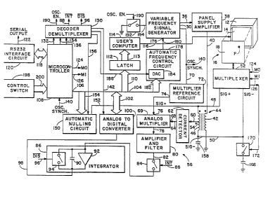
As shown in Fig~ 1, a touch panel device in
2S accordance with the invention has a display unit 12
with a display screen 14. The illustrated display
unit comprises a cathode-ray tube computer terminal
and, accordingly, the display screen 14 comprises the
face of the cathode-ray tube. An optically-transparent
touch panel 16 is positioned to overlay the screen 14
so that the screen is visible through the touch panel.
By optically transparent, it is meant that it is
possible to perceive images on screen 14 through the
touch panel 16. In other applications, the display
unit 12 is eliminated. For example, an inormation
~2~3~
- 12 -
containing sheet of paper, such as a question and
answer sheet, may be positioned underneath the touch
panel lS with the touch panel being utilized to enter
- data relating to the guestion and answer sheet~ In
certain applications, the touch panel 16 need not be
- transparent~ For example, the touch panel may simply
be used as a data entry pad with the location touched
causing the ~ntry of data inko a computer or other
device.
The touch panel 16 has a base plate, which
may be of glass or other optically transmissive
material, with an elec rically-conductive coating 18
over its outer surfaceO The coating 18 may cover the
entire display screen 14 when the touch panel is in
place, or only that portion of the screen 14 which is
used to display user-selectible items.
As shown in general in Fig. 2, and described
in greater detail below, the coating 18 comprises a
touch sensitive or sensing surface with plural
electrical contacts or electrodes, in this case twenty
such contacts A through T. A f irst set 22 of these
contacts, that is contacts P through T, is positioned
in a row at one side of the touch sensing surface 18.
A second set 24 of contacts, contacts F through J, is
positioned in a row at the opposite side of the touch
sensing surface from the first set. That is, the
firæt and second sets 22, 24 are in rows spaced apart
from one another in a first direction across the
surface 18. A third set 28 of such contacts, contacts
K through O, is positioned along the lower or third
side of the surface 18. In addition, a fourth set of
such contacts, contacts A through E, is positioned
along the fourth or upper side of the surface. Thus,
the third and fourth sets of contacts are spaced apart
from one another in a ~econd direction across the
~3~
- 13 -
touch panel surface. The contacts may comprise air
dried silver contact paint spots, approximately 002
inches s~uare. Respective leads are coupled to the
- contac~s to facilita~e convenient electrical
connection to the contacts. To provide strain relief,
- the portion of each of these leads adjacent to its
associated contact may be secured~ as by epoxy, to the
edge of the touch panel base plateD
With this construction, the first and second
sets 22, 24 of contacts are at the opposite
horizontally separated peripheral side ed~es of the
~ouch panel. The other set~ 26, 28 of contacts are
vertically ~paced apart at opposite peripheral side
edges of the touch panel. Although the contacts of
each set do not necessarily have to be in a line, when
colinear and when the first and second directions are
normal to one another, the contacts define a reference
coordinate system. Touch locations are determined
relative to this coordinate system by the circuitry
explained below. Moreover, when the touch panel is
mounted and calibrated, the contacts are at known
locations relative to the terminal screen 14.
Therefore, by determining a touched location on the
touch sensing surface 18, a corresponding
determination is made of the location on the display
terminal screen 14. It should be noted that the
invention is not limited to this particular contacting
scheme. Moreover, a greater or fewer number of
contacts may be used along each side of the touch
sensing surface.
The touch locating ~ystem illustrated in Fig.
2 utilizes the two pairs of opposed sets 22, 24 and
26, 28 in determining the touch location relative to
the two directions across the touch sensing surface.
Only one pair of opposed sets is used if single
s ~
~3~
- 14 -
direction touch location determination is to be made.
That is, set~ 22 and 24 are used to determine touch
location in the first or X direction. Also, sets 26
- and 28 are used to determine touch location in the
second or Y direction.
With further reference to Figs. 1 and 2, a
function generator or signal source 30 generates an
alternatiny current voltage touch panel scanning
signal at an output 36. A panel driving amplifier 38
receives the panel scanning signal, amplifies this
signal, and applies the resultant signal on an output
40 to the primary winding 42 of a touch panel driving
transformer 44. This drives the secondary winding 46
of the trans~ormer and establishes an alternating
current voltage across the secondary winding between
its signal plus (SIG~) output 48 and its signal minus
~SIG-) output 5G. A multiplexer or switching circuit
52 applies the panel scanning signals ~rom outputs 48
and 50 of the secondary winding to selected sets or
rows of the touch panel contacts as explained below.
In response to these scanning signals, panel output
touch signals or touch current signals are generated
at the center tap 54 o the transformer 4~ when the
touch sensing surface is touched. These touch curre~t
signals are processed by a panel output signal
processing circuit means 56 to provide an indication
of the location of touch and other information.
In the illustrated panel output signal
processing circuit 56, the touch current signals from
center tap 54 are transmitted along a line 60 to a
touch current detector 62, such as a current sensing
operational amplifier. The output of amplifier 62
corresponds to the touch currents at the center tAp
54. The amplifier 62 output is fed on an output line
64 through a filter 66 (Fig. 3) and then to one inpu~
æ~
~ 15 -
68 of an analog multiplier 69~ The signal generator
30 has an alternating-current voltage reference output
which is coupled by a line 70 to a multiplier
- reference circuit 72. Multiplier reference voltage
signals from the reference circuit are applied on a
- line 74 to a reference input 76 of the analog
multiplier. The reference output signals synchronize
the multiplication by multiplier 69 with the
alternating current voltage signals applied to the
touch sensing surface 18~
The resulting multiplied touch current
signals are transmitted along a line 78 to an
amplifier and filter circuit 80. The output of
circuit 80 is fed on a line 82 through an integrator
timing ~witch 84 and to an integrator circuit 86,
which integrates these signals. The integrator timing
switch 84 is closed during integration time periods in
response to integration timing ~ signals generated
as explained below and applied to an integrator timing
input 88. When switch 84 closes, signals delivered to
integrator circuit 86 are integrated therein. The
integrator circuit includes an integrating capacitor
90 in parallel with an amplifier 92. In addition, an
integrating capacitor discharge switch 94 is insluded
for selectivèly discharging integrating capacitor 90
in response to discharge ~DXS) signals on a line g6.
The~e discharge or integrator zero signals are
generated as explained below. The integrated touch
current signals are ~ed on a line 98 to an analog to
digital converter circuit 100 which digitizes these
signals. These digitized signals are transferred
along data busses 102, 104 to data inputs 106 of a
microcontroller 108. The microcontroller, among other
functions, computes the touch location and other
desired information from the touch current signals.
g~
- 16 -
The microcontroller 108 interacts via bus
104, a bus 110, a parallel output latch 112, and a bus
113 with a computer 114. Computer 114 i~ connected by
- a line 116 to the display terminal 12. For an example
5 of such interaction, computer 114 may cause selected
information to be displayed on the screen 14. Also,
computer 114 may change the displayed information, as
determined by software, depending upon the touched
location. This is ~ccomplished in a conventional
10 manner to fit the desired application. The
microcontroller 108 is also coupled by a bus 118 to a
conventional RS232 telecommunications interface
circuit 120. This permits the touch panel to
communicate over a telecommunications network with
15 remote data processing stations. Typically, a serial
output 122 is provided from the interface circuit 120.
Control signals from the microcontroller 108
are transmitted at respective M0 and Ml outputs along
lines 124, 126 to the multiplexer 52. These control
signals cause the multiplexer to route the panel
scanning signals to desired sets of contacts.
Therefore, touch current signals are generated from
which touch locations may be determined. Exemplary
scanning sequences are discussed below.
The Fig. 1 panel output signal processing
circuit 56 also include& a decoder demultiplexer
circuit 130. Decoder 130 decodes input signals on
lines 132, 134, and 136 from the microcontroller and,
in response thereto, generates signals which control
various ~unctions of the touch panel circuitry. For
example, decoder 130 generates the integration timing
signals (INTJ fed to line 88. Upon receiving these
signals, switch 84 closes so that integration
commences when touch location determinations are
desired. Integration continues for the duration of
- 17 -
the INT signal. The decoder circuit also generates
the integration capacitox discharge signals ~F-) on
line ~6. These signals cause switch ~4 to close so
- ~hat integration capacitor 90 is discharged prior to
each successive integration. The microcontroller has
a synchronization input which receive~ synchronization
signals on a line 140 derived from the reference
output of signal source 30 Consequently, integration
is synchronized with the application of panel scanning
signals to the touch sensing surface 18. The decoder
circuit also has an output coupled by a line 142 to
the analog to digital converter 100 for controlling
the delivery of digitized integrated touch signals
from converter 100 to the microcontroller 108.
More accurate determination of touch currents
and touch locations result when the analog to digital
converter is providing an output of a magnitude which
is within a desired range. If too small, minor
variations in touch currents can be overlooked and
spurious signals have a greater impact. If too large,
the analog to digital converter may overflow and
provide an inaccurate touch current indication. To
minimize such possibilities, microcontroller 108
monitors the magnitude of the analog to digital
converter output~ When outside a desired range,
microprocessor 108 adjusts the duration of an
integration timing control signal sent to decoder
1300 In response, the decoder adjusts the duration of
the INT signal, and thus the integration time period,
to bring the analog to digital converter output to the
desired level. This facilitates the use of the touch
panel device under widely varying conditions with
accompanying widely varying touch currents. For
example, in situations in which a stylus iæ used to
touch the touch sensing surface 18, an individual
.,
.~.
,
, ~
- 18 -
touches the touch sensing surface with a bare finger
or other body part, or even if the individual touches
the touch sensing surface with a gloved finger.
- A nulling circuit 150 is utilized to adjust
touch current signals a~ the center tap 54 to a null
or zero value at times when the touch sensing surface
18 is not being touched. After nulling, the existence
of currents at center tap 54, at least currents above
a noise threshold level~ indicate the presence of a
touch. In general, nulling circuit 150 automatically
provides a suitable offset current at center tap 54 to
counteract or nullify any current signal at the center
tap under no ~ouch conditions.
The Fig. 1 form of automatic nulling circuit
accomplishes this by selectively coupling an effective
capacitive load to one of the panel scanning outputs,
in this case, via a line 152 to the SIG~ output 48.
The nulling circuit 150 responds to nulling signals
from mirrocontroller 108 which are delivered on bus
104 and a bus 154 to an input of the automatic nulling
circuit. The magnitude of the effective capacitive
load coupled to the SIG+ output 48 by the nulling
circuit is varied in response to the nulling signals
to thereby effect nulling. Typically, an offset
nulling capacitor 158 is coupled to the SIG- panel
scanning output 50 to provide initial offset to the
center tap touch current signals in a direction
opposite to the offset provided by the automatic
nulling circuit. Consequently, as capacitance is
added by the automatic nulling circuit to the SIG+
panel scanning output, the initial o$fset provided by
capacitor 158, and from other ambient signals are
balanced. Another offset capacitor 168 is seleatively
coupled by a switch 170 to the SIG- panel scanning
output 50. Switch 170 is closed in response to a
~ - 19 ~
siynal on a line 172 from multiplexer 52 during
impedance touch current determinationsO When bvth of
the capacitors 158 and 168 axe coupled to the circuit,
- the initial off et is higher because higher current
7eakage typically occurs during impedance touch
current d~terminations.
The touch panel circuit 56 of Fig. 1 also
includes an automatic frequency control means for
shifting the frequency of the panel scanning signals
to levels which are unaffected by fixed frequency
interference spectra, such as cathode-ray tube
horizontal flyback signals, in the environment in
which the touch panel device is used. In this
description, the phrase "fixed frequency interference
spectra" refers to periodic signals and their
harmonics of the type typically generated by equipment
used with the touch panel device. This term
encompasses signals which are fixed for a time and
then changed to another fixed value, such as the
variable and multiple horizontal flyback signals in
some cathode-ray tube displays~ It also includes
ambient noise signals which vary at a rate which is
slower than the rate at which the touch panel device
is capable of adjusting the.panel excitation
frequencyO Operation of a touch panel device at or
near such fixed frequency interference spectra
severely degrades touch location determination and, in
some cases, makes such determination totally
unreliable.
In the Fîg. 1 form of the invention, the
signal generator 30 comprises a variable frequency
~ignal generator. Thi~ signal generator has a
frequency control input 176. Signal generator 30
comprises means for producing alternating current
voltage outputs on lines 36, 70 of a frequency which
- 20 -
is variable and controllable in response to frequency
control signals at the frequency control input 176.
Under the control of microcontroller 108 9 an automatic
- frequency control circuit 178 generates the fre~uency
5 control signals and delivers such signals on a line
180 to the frequency control input 176. ~ore
specifically, at times microcontroller 108 determines
that frequency adjustment is needed, digit~l fre~uency
control signals are delivered on bus 104 and a bus 182
to the automatic freguency control circuit 178.
digital to analog converter 184 respcnds to signals
from line 186 of decoder 130 to transfer the frequency
control signals from bus 182 to the automatic
frequency control circuit. Typically, a frequency
adjustment is made when nulling adjustments become too
frequent, the object being to shift the operating
frequency to a level which reduces the rate of nulling
adjustments. The microcontroller also predetermines
the direction, upwardly or downwardly, of the
frequency changes.
The touch panel device of Fig. 1 al~o
includes features for protecting the circuit 56, as
well as the touch sensing surface 18, from exces~ive
touch currents. Specifically, assume microcontroller
108 determines that the touch c~rrents are in excess
of a maximum safe threshold and that the integrator B6
is integrating for its minimum integration time
period. In this c~se~ the microcontroller causes
decoder 130 to shut off an OSC. EN. output on a line
190. This causes a switch 192 to close and grounds a
signal generator disable input 194 of source 30. When
this happens, the signal generator output terminates
so that panel scanning signals to the touch sensing
surface 18 are interrupted. For added protectlon, the
M0 and Ml outputs from microcontroller 108 are shifted
~ '
- 21 -
to digital logic levels which control multiplexer 52
to open the connections hetween the SI~-~ and SXG-
panel scanning outputs and the touch sensing surface.
- A manually operated control switch 198 is
coupled to the microcontroller 108 by control lines
200. As explained more fully below, the settings of
switch 198 designate processing parameters, such as
whether touch location signals are to be delivered at
the parallel output 113 or the serial output 122.
lQ Panel Scannin~ Sequences and Touch
Location Determination
As explained in greater detail below,
microcontroller 108 controls the multiplexer 52 so as
to repetitively apply the transformer SIG~ and the
SIG- outputs 48, 50 to selected sides of the touch
sensing surface 18 in a predetermined sequence. From
the resulting touch currents, the touch location and
other information is determined.
As a first specific example of a scanning
sequence, and with reference to Fig. 2, assume that
the touch currents have been adjusted to zero by
nulling circuit 150 when the touch sensing surface is
untouched. Also, assume that an X-Y coordinate system
has been established with its origin at the center of
the touch sensing surface. If a point P is touched,
the location of this point is given by the coordinates
X and Y as shown in Fig. 2 (al~o sometimes indicated
herein as Xp, Yp).
In a first mode of this first scanning
sequence, the SIG- output 50 is coupled to the set of
contacts 22 and the SIG~ output 48 is coupled to the
~et o contacts 24. In additlon, the other sets of
contacts 26 and 28 are open circuited ~although they
need not be). In this mode, an alternating current
gradient is established in a first or X direction
,
.: .
`~ ' ' ,. .
- 22 -
across the touch sensing surface. In this case, the
first direction is horizontal and compri es an X
axis. As explained below, after multiplication by
- multiplier 69 and filtering, the resulting first or X
touch current is ~xpressed by the following equation.
(a) i~ = Kx ~ Zt
In the above equation, ix i~ the resulting touch
current, which may be designated as a first or X touch
current. Also, V is the voltage at secondary winding
output 48 relative to virtual ground at the center tap
of the transformerO In addition, Zt is the impedance
added to the circuit when a user touches the touch
sensing circuit and Kx is a constant. In addition,
the quantity V/Zt corresponds to the impedance current
that flows upon touch by a userl Finally, X is the X
location of touch.
In a second mode of this first ~canning
sequence, the SIG~ output 48 is coupled to at least
one, and typically simultaneously to both, of the
first and second sides 22, 24 of the touch sensing
surface. This establishes a uniform alternating
current voltage in the first direction. In this
mode~ any touch current at the center ~ap 54
corresponds to the impedance touch current through a
user. This impedance ~ouch current iz, after
multiplication and filtering, may be expressed as
follows:
V
~b) iz = - Kz
Zt
In other approaches to the impeda~ce current scanning
. mode, one of the panel scanning outputs ~i.e., the SIG+
output) is coupled to one side only o the touch sensing
surface, to two adjacent sides, or to all four sides.
:
' ' :
.
~o
- 23 -
The above two equations may be combined to
provide the following equation for the X location of
touch:
S ( c ) ~ = x z
lz Kx
To determine the quantity Kz/Kx, one touches the
touch sensing surface at known X locations. For
example~ a the four corners or at the far right and far
left along the X-axis. By substituting the known X
locations in formula (c) above and averaging the
results, a value of K~KX can be de4ermined. Once
Kz/Kx is determined, unknown X touch locations can
be computed from the first and impedance touch current
signals using the abov~ equations.
Assuming two dimensional touch information is
desired, ~he first scanning sequence includ~s a third
mode~ In the third mode, the SI~ output 48 is coupled
to top side 26 o the touch sensing ~urface and the SIG-
output 50 is coupled to the bottom side 28 of the touchsensing surface. This establishes an alternating
- current voltage gradient in the second or Y direction
across the touch sensing surface. The resulting second
or Y touch current, i~, after multiplication and
filtering, is expressed by the following equation:
(d) iy - Ky Y Vzt
In the above equation, Y is the Y location of toucb. In
addition, Ky is a constant which may be determined in
the same manner as Kx. In the Fig. 1 form of the
invention, Ky, Xx and Kz are each approximately
equal to one. Therefore, there is no need to determlne
these cons~ants. Combining formulas (b) and (d) above
results in the following expression of Y location:
(e) Y = Z
lS Xy
... ..
' ,,:,'"~ ' ,. '.. . . .
- 24 -
In this expression, Kz/Xy is a constan~ which may be
determined in the same ~anner as Rz/Kx~
Thus, in the above manner the X and Y
- coordinates of touched location P can be de~ermined
from touch currents generated by scanning ~he touch
- sensing surface in the three modes described above.
By repeating the scanning cycIe a predetermined number
of times and combining or averaging the results, an
accurate determination of touch position can be
obtained. However, although less accurate, touch
location can be determined with sufficienk preci~ion in
many applications without averaging. The switching of
the scanning signals between the various modes is
accomplished by multiplexer 52 under the control of M0
15 and Ml signals from the microcontroller 108. The
location o~ touch on the touch panel 16 identifies, to
the computer 114, which informational item being
displayed on the terminal 12 has been ~elected by ~he
user. The terminal 12 then responds in a known manner
to this determination of user selection.
In addition to determining touch location,
additional information may be obtained from the
generated touch currents. For example, the X and Y
coordinates may be computed at successive times with the
impedance touch current iz also being monitored. If X
and Y do not vary, but iz varies, this indicates that
the user is continuing to touch a particular location on
the touch sensing surface, but has changed the manner of
touching this location. For example, the user may be
pressing his or her ~inger harder at the touched
location. This varies the area of the touch ~ensing
surface which is touched. The resulting variation in
impedance touch current can be used by computer 114 for
control of addîtional functions. For example, if the
touch screen is pressed at the same loca~ion, but only
.. ' ' " ' .
wa
25 -
harder, the sesulting Ghange in impedance touch current
iz is detected and can be used to call up a particular
subroutine which operates on data identified by the
- touched location.
Another scanning sequence wbich provides
~ desired X and Y touch currents, as well as impedance
~ouch currents, is as follows. This second sequence
involves scanning the touch sensing surface in four
modes instead of the three modes previously describedO
10 With reference to Fig. 2~ this scanning method is
described with reference to a touch point P identified
by Xl~ X2, Yl and Y2 locations. That is, the
total distance in the X direction across the touch
sensing surface is known and is equal to the sum of X
and X2. Also, Xl is defined as the horizontal
distance from the left side of the panel in Fig. 2 to
point P while X2 is the horizontal distance from the
right side of the panel to point P. Moreover, the total
distance in the Y direction across the panel is known
and equal to the sum of Yl and Y2. Also, Yl i5
the distance from the lower side of the touch sensing
urface to point P while Y2 is the distance from the
upper side of the touch sensing surface to point P.
In the first mode of this second scanning
se~uence, the multiplexer 52 is configured to couple the
SIG+ output 48 to the right side of the touch fiensing
surface while the center tap 54 i8 coupled to the left
side of the touch sen~ing surface. This establishe~ an
alternating current voltage gradient acro5s the touch
sen ing surface in the X direction from right to left.
Assume that the nulling circuit bas been adjusted ts
null the touch currents to zero when the touch sensing
~ surface is untouched. Also assume that multiplication
and filtering has been performed. Under ~-hese
conditions, a first touch current iXl at the center
- 26
tap i5 expressed as follows:
X
(f) iXl ~ Kx Xl ~ X2
In addition, when in a second mode, the SIG~ output 48
is applied to the left side of the touoh sensing surface
and the center tap 54 is coupled to the right side o the
touch sensing surface. This also establishes an
alternatin~ current voltage gradient in the X
dir~ction, but from left to right. In this case, and with
the above assumptions, a second touch current iX2 is
expressed by the following formula:
- 2.. V
(g) iX2 = Kx Xl ~ X2 Zt
When formulas (f) and (g) are added, the impedance kouch
current izx is given as follows:
(h) RX~t = (iXl + iX2~ z~
~ Finally, combining formulas (f) and (h) results in the
following expression for Xl, the X-axis position of
touch point P:
(i) Xl ~ ~1~ 2)
In the above e~uations, RX is a aonstant and can be
determined in the same manner as explained above by
touching the touch sensing ~urface at known locations.
In addition~ as prevlously mentioned, the sum Xl plus
X2 is known. Therefore, from the above two
measurements, X-axis position information for touch
polnt P can be calculated. Also, information is
obtained concerning changes in the impedance touch
current izx.
The Y-axis pos~tion information is determined
in the following manner. In the third mode o~ this
" ~. "
a~so
- 27 -
second scanning sequence, the SIG~ output 48 is coupled
to the top side of the touch sensing surface while ~he
center tap 54 is coupled to the bottom side of ~he ~ouch
- sensing surface. The resulting third touch current
S iyl is expressed as follows:
(~) lyl ~ ~Y Y2 ~ Yl Zt
In the fourth mode, the SIG+ output 48 i5 coupled to the
bottom side of the touch sensing surface while the
center tap is coupled to the top side of the touch
sensing surface. This results in a fourth touch current
iy2 expressed by the following equation:
,, Y~, ,V,
(k) iy~ ~ Ky -- _
By combining formulas ~;) and ~k), the following
expression for impedance touch current izy is obtained:
~1) Ky Zt- (iyl ~ iy2) ~ izy
Furthermore, when formulas (j) and (1) are combined, an
equation for Yl i5 obtained:
(m) Yl = iyl (Yl + ~2)
2S ~iyl + 1 ~
As explained above, the sum Yl plus Y2 is known. In
addition, the constant ~ can be determined in the
same manner as the constant Kx. Thus, the Xl and
Yl position~ can be obtained from the touch currents.
In addition, changes in the impedance touch current can
be monitored as desired.
A5 will be apparent to those skilled in the
art, other scanning se~uences and modes of establishing
alternating current gradients across the touch ~ensing
~urface may be employed to generate the touch signals or
..
~æ73~
- 28 -
currents from which the desired location information can
be determined.
S~
- Again referring to Fig. 2, the ~ouch panel 16
has a touch sensitive surface 18 which extends across
- the area thereof which, in conjunction with a location
determination circuit, is used to sense touch by a
user. As previously mentioned, the touch panel 16
includes a base plate coated on a surface 18 with an
electrically conduc~ive ilm. One suitable example of
such a film is indium tin oxide (10~ indium, 90% tin
oxide) having a sheet resistivity of ~0~ ohms per square
and a transmission of 85% for light at 520 nanometers.
Such plates are commercially available, such as from
Optical Coating haboratory (OCLI) of Santa Rosa,
Caliornia. The sheet resistivity of the film is not
highly critical, with resistivities of 50 to 2j000 ohms
per square, or higher, being suitable. Sheet
resistivities significantly below 200 ohms per square
~0 may require special low resistance switches and can
result in relatively high power consumption.
The base plate is not limited to any particular
shape. Thus, it may be circular, concave, spherical,
curved or ~lat to fit the screen 14. In addition, the
base plate may be opa~ue or optically transparent and of
a variety of suitable materials. To reduce glare from
reflected light from background ~ources, the base plate
may be of a commercially available anti-glare glass.
This glass may also be flat or contoured to match the
curvature of the display screen. One source of such
base plates is Eagle Convex Glass Co. of Charlesburg,
West VirginiaO
As previously mentioned, the particular
contacting scheme employed may be varied as exemplified
by the approaches mentioned above. Of course, the
'; .
~x~
- 29 -
specific multiplexer or swi$ching circuit 52 will vary
depending up~n the contacting arrangement which is
chosen. In general, any contacting arrangement may be
- employed which facilitates the establishment of a
selatively uniform alternating current voltage gradient
~ across the touch sensing surface in the desired
directions "
Touch Panel Excitation Circuit
The details of the circuit utilized for
generating and applying alternating current voltage
signals to the touch sensing surface 18 are shown in
Fig. 3.
More specifically, in the illustrated form,
signal generator 30 typically comprises a conventional
sine wave signal source, such as an integrated circuit
XR 8038A source from Exar Company~ connected in a
conventional manner as shown in Fig. 3, Source 30
provides a sine wave output at pin 2, which is the
output 36. Although not critical, the circuit is
typically operated at a signal generator output
frequency of from 15 kilohertz to 300 kilohertz9 with
200 kilohertz being suitable. For reasons explained
below; this frequency is automatically adjustable by the
touch processing circuit. The ~ignal source 30 also
provides a square wave reference signal at pin 9
(output 70). This reference signal is used to generate
synchroni~ation signals at OSC. SYNC~. line 140 and al~o
by the multiplier reference circuit 72 to provid~
reference voltage signals for analoy multiplier 69.
The illustrated driver amplifier circuit 38
includes an operational amplifier 210 with a discrete
push-pull follower circuit 212. The output of driver
amplifier 38 is coupled by line 40 through a one
microfarad ceramic DC blocking capacitor 213 to the
primary winding 42 of transformer 44. Capacitor 213
- 30 -
prevents the transformer 44 from belng driven into
saturation by DC currents. Typically, the signal
generator and driver amplifier combination drives
- transformer 44 so as to provide an approximately 12 volt
5 peak to peak voltage across the secondary windings 48~
~ 50 of the transformer. The same voltage appear~ across
primary winding 42 because the specific ransformer
being used has a one-to-one primary to seccndary voltage
ratio.
In ~he preferred form, transformer 44 has a
toroidal core. This transformer isolates current used
to drive the touch sensing surface 18 from the current
generated by the signal generator 30. Consequently/ the
only currents appearing at the center tap 54 are touch
15 currents. With such a transformer driving configuration,
circuit complexities associated with subtracting panel
scanning signal currents from touch currents are
eliminated.
Suitable resistors and capacitors utilized in
the signal generator and driver amplifier circuits, and
which have not been mentioned above, are set forth in
Table 1 at the end of this detailed description.
Multiplexer 52 (Fig. 2) comprises a switching
circuit for applying the panel scanning signals to the
touch sensing surface. These panel scanning signals are
applied 80 as to establish the alternating current
voltage gradients in the desired directions across the
touch sensing surface. With the illustrated kouch
contacting arrangement, mul~iplexer 52 comprises six
double-pol0 double-throw CMOS analog switches 268O270
together with a state decoder circuit 272,
interconnected as ~hown. As a specific example,
switches 260~270 may compr~se G.E. Intersil IH 5045
switches. Also, state decoder 272 may comprise a
conventional 74LS02 NOR gate set. The scanning signals
~ tra~le n~ a r~
1~7~
- 31
at the SIG+ output 48 and the SXG- output 50 are
delivered to scanning inputs of the multiplexer circuit
52. In general, the switche~ are toggled to various
- states by state decoder 272 in response to control
signals ~0 and Ml delivered to the decoder on control
- lines 124, 126 from the microcontroller 108 ~Figs. 1 and
3). The mult~plexer input~output lines~ designated
generally as 274 in Fig. 3, are connected to the
respective contacts A through T of the touch sensing
surface 18 as shownO
When logic zero MO and one Ml signals are
respectively applied to control lines 124, 126 by the
microcontroller, the switching circuits assume a first
or X kouch current determination state. When in this
first state, the contacts P-T of set 22 are electrically
tied together and the contacts F-J of set 24 are
electrically tied together. In addition, the contacts
A-E and X-O are open. Also, when in the first state,
the SIG~ output ~8 is applied to the contacts of the set
24. In addition, the SIG- output 50 is applied to the
contacts of the set 22. Under these conditions, an
alternating current voltage gradient is established in
the first or X direction across the touch sensing
surface.
~5 In addition, when the M0 control signal
delivered on control line 124 is a logic one and the Ml
control signal on control line 126 is a logic zero, the
multiplexer is in a second or Y touch current
determination state. In this second state, contacts A-E
of set 26 are tied together and to the SIG~ output 48.
In addition, the contacts K-O are tied together and to
the SIG- output 50. Furthermore t the contacts P-T and
F-J are open. Under these conditions t an alternating
current gradient is established between the top and
bottom sets of contacts in a second or Y direction
across the to w h sensing surface.
- 32 -
The multiplexer is in a third or impedance
touch current determination state when both the M0 and
~1 control signals are at logic zero. When in this
- state, contact set 22 and contact set 26 are
electric~lly tied together and to the SIG~ output 48.
Also, ~he remaining sets of contacts 24, 28 are open.
The alternating current voltage is then simultaneou~ly
applied to two adjacent sides of the touch sensing
surface. As a result9 any touch current which flows at
the center tap 54 corresponds directly to the impedance
current generated when the touch sensing surface 18 is
touched by a user. By adding an additional CMOS analog
switch of the type shown, all sides of the ~ouch panel
can be simultaneously driven by the same signal. Also,
impedance current can be determin~d in many cases with
only one side of the touch sensing surface being
driven. of course, other contacts may be energizea with
the goal being the establishment of a uniform
alternating current voltage field throughout the touch
sensing surface.
Finally, the multiplexer is in a fourth or off
state when both the U0 and Ml signals are logic ones.
When the switches 260-270 are in the off state, the
application of the panel scanning ~ignals to the touch
sensing surface is interrupted. Shifting to the off
state can be done when excessive output currents are
detected. This protects the touch sensing surface and
ci~cuit from these currents. Also, for circuit
protection purposes, khe switches are typically switched
off between 8hifting of the panel between X, Y and Z
states and al50 when the circuit is reset.
The following state table illustrates the above
states. In thi~ table, the letters T9 B~ R and L
correspond to the outputs of~state decoder 272 and
re~pectively to th~ top, bottom, right and left sides of
touch ~ensing surface 180
33 -
~TA~E ~ABLE
~ Panel Side-~
0 0 1 0 1 0 Off Sig+ Sig+ ~f~ Third or (Z)
~ 1 1 1 0 0 Sig Sig+ Off Off First or (X)
1 0 0 0 1 1 Off Off Sig~ Slg Second or (Y)
~ 0 0 ~ Off ~ff O~ Off
lQ
In operation, the microcontroller 108
repeatedly cycles the scanning of the touch sensing
surface 18. This is accomplished by shifting the
multiplexer between states in the following ~equence
for each cycle: Third - Off - First - Off - Second -
Off - Third - Off. Overcurrent testing is typically
performed during the Z state and in this sequen~e is
checked at the start and end of each scanning cycle.
Also, since impedance current is used in determining
both X and Y position, it is desirable to update Z
current determinations with greater frequency than X
and Y current determinationsO Other scanning
sequences are of course suitableO The resulting touch
current signal~ are then combined pursuant to the
equations (a)-(e) above to determinè touch locations.
Typically, the multiplexer ~yale ~or scanning through
all tbree states i8 relatively rapid (30 to 1,000
hertz). In general, the ~lower the multiplexer
~requency, the longer it takes the processing
circuitry ~o determine a touch location.
In a similar manner, a suitable multiplexer
may be used to generate the ~our touch currents iXlt
iX2, iyl and iy2 as explained above ln
connection with equations jf)-(m).
,
' :
' ~
- 34 -
Although a transformer driven touch ~ensing
circuit simplifies the circuitry and provides other
advantages, other circuits for establishing the
- desired alternating current voltage gradients across
the touch sens.ing surface may be used. For example,
the sinusoidal drive signal output at 40 may be fed
through a unity gain inverting amplifier to the SIG-
outpu 50~ Simultaneously~ the output at 40 may be
fed to the SIG~ output 48. The differential currents
at the SIG~ and SIG- outputs are then ob~ained by a
differential current detector and processed to
determine touch locationsO Moreover, when the touch
panel is untouchèd t and when the nulling circuit 150
has been properly adjusted to the null, as explained
below, the differential current is ~eroO
As an added protection feature, the touch
panel application circuitry of Fig. 2 includes
optional means for establishing a discharge path for
discharging high voltages from the touch sensing
circuit. These voltages may, for example, result from
static electricity from a user o~ the device. In the
illustrated form, this means comprises four sets of
clamping diodes, one set being numbered 280 in
Fig. 2. Each set is electrically coupled to a
respective ~ide of the touch sensing surface. For
example, set 230 is connected to the mid-contact C at
~he top of the panel. Similarly, the other sets are
connected to the mid-contact at the other ~ides of the
panel. Set 280 includes a first diode 282 having its
cathode connected to the touch sensing surface and its
anode connected to a negative 12-vol~ DC supply used
in the touch panel device. ~ second diode 284 has its
anode connected to the touch sensing surface and its
cathode connected to a positive 12-volt DC supply.
Whenevsr the voltage at the top side of the panel
. ....... .
- 35 -
exceeds 12 volts, plus the biasing voltage of diode
284, diode 284 conducts and discharges this voltage~
Similarly3 whenever the voltage drops below a negative
-- 12 volts and the biasing voltage of diod2 282, this
diode conducts to also discharge the panel.
- Consequently, the voltage at the touch sensing surface
is effectiv~ly limited to a range of plus or minus 12
voJts. A first zener diode 285 has îts anode
connected to the negative 12-volt supply and its
cathode grounded. A second zener diode has its
cathode connected to the positive 12-volt supply and
its anode grounded. These zener diodes have a
break-down voltage which is higher than the magnitude
of the supply voltages, for example, 18 volts.
Consequently, any voltage discharged through diode set
280, as well as the other diode sets, in excess of
what can be dissipated by the voltage sources, is
diverted through the zener diodes to ground. In
addition to high voltage protection, these clamping
diodes and zener diodes do not draw excess current
duriny normal touch location detection. Therefore,
the accuracy of touch determinations is not af~ected
by leakage currents through this protection circuitry.
With continued reference to Fig. 2, circuitry
for coupling offset capacitor 168 to the SIG- output
50 during third or 2 stage touch current determination
i8 shown. More specifically, the MO and Ml outputs
are coupled to switch 170 by a wired OR gate comprised
of diodes 28B, 290 and resistor 29~. Switch 170 is a
conventional inverting switch which closes when lts
control input is zero. Thi~ happens when M0 and Ml
are both at logic zero and the panel is in its third
or Z impedance current determination state. The
functioning of offset capacitor 168 i8 explained below
- 36 -
in connection with the description of the automatic
nulling circuit 150.
- Referring again to Figl 3, current detector
62 may comprise a current-to-vvltage converter
- operational amplifier with its inverting input
connected to the center tap 54 of the transformer 44.
The noninverting input of amplifier 62 is grounded. A
pair of input diodes are connected in parallel and in
opposite directions across th~ inputs of current
sensing amplifier 62. These diodes protect the
amplifier from excessive currents and voltages. A 220
ohm feedback resistor 302 is connected between the
output 64 and inverting input of amplifier 62. When
connected in this manner, amplifier 62 provides an
output 64 corresponding to the currents flowing to the
transformer center tap 54~ and thus to the first,
second and impedance touch currents. These touch
current signals are filter~d by a $ilter circuit 66
and delivered to input 68 of the analog multiplier.
Filter 66 comprises a pa~sive, high pass filter. This
filter includes a 1000 picofarad DC blocking capacitor
304 and a 4.7 kilohm resistor 302 connected from
analog multiplier input 68 to ground. The negative
12 volt supply i~ al50 connected through a 4.7 kilohm
resistor 306 to the input 68.
Analog multiplier 69 obtains a reference
signal from the output 70 of signal source 30.
Output 70 is a square wave output which is shifted in
phase 90 from the sine wave output 36 used to drive
the transformer 44. Output 70 is connected through a
4.7 kilohm resistor 310 ~o a node 311, which in turn
is connec~ed through a 10 kilohm resistor 312 to the
positive 12 volt ~upply. Node 311 is also grounded
through a 3.9 kilohm resistor 314. This network
. .
~ ,
. ...
.,
~o
37 -
divides he voltage at the square wave output to a
level which is compatible with TTL logic. A diode 316
clips the negative half cycles of the square wave
- output. This leaves the positive half cycles as the
synchronization signals at OSC. SYNCHo output 140.
~ Node 311 is coupled by a 1000 picofarad DC blocking
capacitor and a pair of 10 kilohm resistors 320, 322
to the input 76 of the analog multiplier 69. A 150
picofarad filtering capacitor 324 is connected from
the node between resistors 320, 322 and ground. Also~
input 76 to the analog multiplier is grounded through
a one kilohm resistor 328. These latter resistors and
capacitors filter the clipped square wave output to
provide the reference frequency signal for the analog
multiplier. Analog multiplier 59 may comprise an
MC1496 analog multiplier available from Motorola
Company. This circuit is connected as shown in Fig. 3
and has conventional biasing resistors listed in
Table 1.
With the circuit nulled, as explained below,
the transformer secondary center tap is at exactly
zero volts, in the absence of touch by user. This i8
true even without the sensing circuit. A touch by a
user diverts some current to ground. Conservation of
charge requires that this current also flow in the
center tap wire 54. The resulting center tap curren~
is composed of a signal at the panel drive ~requency
wO, and a substantial noise component. X, Y and Z
touch data are represented by amplitude changes in the
current signals. Since only the amplitude data is sf
interest, a synchronous detector can be used to
demodulate the amplitude-modulated touch cuxr~nt
signals. Analog multiplier ~9 is used for this
synchronous detection, resulting in enhanced noi~e
rejection and thereby more aacurate touch location
- 38 -
determinations. To accomplish demodulation, the
center tap current ~iynal is multiplied by the aarrier
signal derived from the output 70 of signal source
- 30. Mathematically, in the first or X determination
state and assuming the touch presents a constant
- impedance to ground~ Zt~ the resulting voltage~ are
as follows:
PANEL VOL~AGE:
x~7 &osw ot
CENTER ~AP CURRENT
15xV ocoS (W ot~) ~ Noise
Zt
ULTIPLIER OU~PUT
205 xV0 + cos ~ xVoC052W ot + Noise
2Zt 2Zt
These expressions also include constants which are
cancelled during signal processing. Similar
expressions are obtained during Y and Z touch curxent
determinations. As long as the touch current phase
shift ~ is not ninety degrees relative to the
multiplier reference signal, cos o is not equal to
zero and the multiplier output provides usable data.
Although touch current is typically capacitive,
because the source 30 has a ~quare wave output shifted
- ninety degrees from the ~ine wave output, ~ is close
to zero degrees and accurate inormation is obtained.
Multiplier output amplifier and filter circuit 80
~ 3~ - .
comprise a low pass f.ilter which effectively
eliminates ~he Vocos2wOt term and much of ~he
noise. The r~sulting signals correspond to ix, iy
and iz as set forth in equations a~ b and d above.
Touch location is then determined by processing the~e
- signals.
More specifically~ output pin 9 of analog
multiplier 69 is connected through a 47 kilohm
resistor 346 to the inver~ing input of an operational
amplifier 348, Outp~t pin 6 of analog multiplier 69
is connected through another 47 kilohm resistor to the
noninverting input of the operational amplif ier . This
noninverting input i~ also coupl~d to ground through a
47 kilohm resistor 352. In addition, a 47 kilohm
feedback resistor 354 is connected from the output of
amplifier 348 to its inverting input. Finally, 0.022
microfarad capacitors 356, 358 respectively couple
pins 9 and 6 to ground.
Because Zt varies widely, signal levels at
output 82 vary consider~bly~ If ix, iy and iz
from output 82 were simply converted to digital data
and then divided pursuant to equations a, b and d
above, accuracy would be low for small signals,
because of round-off error~ Instead, the signals are
integrated to give the values txiX, tyiy~ and
tziz. The integration times tx, t~, and tz
are controlled by microcontroller 108 to maximize the
magnitude of th~ integrated values, within limits, and
to minimi~e error. Since t~, ty, and tz are
known by the microcontroller, dif~ering integration
times are factored out by the micro¢ontroller during
touch location determinationO Integration also
provides additional noise filtering.
Referring again to Fig. 3, the amplifier
3s output R2 i5 ed through a 2.2 kilohm resistor 360 to
~ 40 --
the integrator switch 840 Wh~never a logic zero hold
signal is applied on line 88 from decoder 13~, under
the control of microcontroller 108, the switch 84
- closes~ As a result, the amplifier output 82 is
coupled to the integrating capacitor 90. ~he
amplifier output 82 is integrated for an integration
time period having a duration which is determined by
the duration of the hold signal. Integrating
capacitor 90 comprises a 0.022 microfarad capacitor
connected from the inverting input of integrator
amplifier 92 to the amplifier output 98~ The
noninverting input of amplifier 92 is grounded through
a 2.2 kilohm resistor 362. The integrator discharge
switch 94 is in parallel with the capacitor 90 with a
390 ohm discharge current limiting resistor connected
between the integrator output 98 and the switch. In
response to logic æero DIS signals on line 96, from
decoder 130 under the control of microcontroller 108,
switch 94 clo~es to discharge capacitor 90. Discharge
takes place just prior to integration. The output 98
from integrator circuit 86 is a positive or negative
analog voltage. This output corresponds to an
int~grated analog ver~ion of the touch currents
generated at the center tap 54 of the transformer 44.
The integrator output 98 is coupled through
an operational amplifier circuit 366 to the data input
pin 6 of the analog to digital converter 100. The
circuit 366 shifts and attenuates the integrator
output 98 in order to match the inpu~ range of the
analo~ to digital converter. Circuit 366 also
comprises another filtering stage. A pair of zener
diodes 388 is coupled from the node between a pair of
resistors 380, 386 and ground. These diodes clamp the
voltage at this node to approximately plus or minus
~o
- 41 -
6.8 volts and limit the range of voltages applied to
the operational amplifier circuit 366.
~ nalog to digital converter 100 may comprise
- a National Semiconducter ADC1001 circuit. The eight
5 output data lines of this circuit are connected by
- lines 102 and 104 to data input/output pins 32 through
39 of microcontroller 108. Analog to digi al
converter 100 has a CS input pin 1 connected by line
142 to decoder 130, an ~ pin 2, a WR pin 3, and an
10 INTR pin 5. Under the control of microcontroller 108,
as is known, these pins are controlled so that, upon
completion of an integration cycle and the resultant
digitization of the integrated touch current ~i~nal,
the digitized current data is transferred to the
15 microcontroller. The values of the resistors and
capacitors coupled to the analog to digital converter
100, and also included in circuit 366 are listed in
Table I.
A two's complement approach may be used in
conjunction with the digitization of negative values
from the integrator. From the sign of the digitized
value, the quadrant of the touch location P is
determined. For example, with an X-Y coordinate
system having an origin at the center of the touch
sensing surface 18, negative X touch current values
indicate touches to the left of the origin.
Conversely, positive X touch current values indicate
touches to the right of the origin. Similarly,
negative Y touch current values indicate touches below
the origin while positive Y touch current values
indicate touches above the origin.
The integration cycles are repeated, with the
microcontroller ~hifting the multiplexer 52 (Fig~ 2)
through its respective states, to obtain successive
digitized first, second and impedance touch current
~o
- 42 -
values. These values are then processed to indicate
the location at which the panel is touched.
The illustrated microcontroller 108 comprises
- a programmable 8751 EPROM microcontroller from Intel
5 Corporation. In addition, decoder 130 csmprises a
~ 74LSl38 decoder/demultiplexer circuit. In addition,
the telecommunication~ interface 120 may comprise a
~ational Semiconductor DSl489 Quad ~ ine Receiver in
combination with a DSl488 Quad Line Driver. In the
depicted configuration, microcontroller pin 10
comprises a serial input port, pin 9 comprises a reset
input which, if at a logic l levelJ resets the touch
detection circuit, and pin 13 comprises an external
interrupt input. Microcontroller output pin 6 is used
for sending a request to send signal, pin 7 is a data
tran~mission ready to ~end signal line, and pin ll
comprises a serial output~ These pins are controlled
in a conventional manner to enable microcontroller 108
to ~end or receive data; via interface 120t over a
telecommunications network. In addition, serial
transmission and reception of data i8 possible.
Parallel output latch 112 may comprise a 74IS377
octal-D flip-flop wîth eight parallel data output pins
and corresponding input pins. Microcontroller 108
controls latch 112 at pin ll. In addition~ the enable
input pin 1 o~ latch 112 i~ connected to an
input/output pin 8 of the microcontroller. In
response to enable signals from the microcontroller,
parallel transmission of data from latch 112 occur~.
Control ~wltch 198 may comprise a manually
operated ~witch having seven outputs connected to
microcontroller input pin~ 21-27. These ouput~ are at
logic l or logic 0 level~, depending upon the switch
settings. Typically, the logic levels at pins 13 and
14 determine the mode or manner by which the existenc~
~ t rc~ c~ ~ ~ ar k
.~ , .. ...
::~ .. ,:, .. ..
::
:
~o
~ ~3 -
of a touch is determined. For example, if hese pins
are at respective logic 0 and 1 levels, a "touch on
makeW mode is indicated. In this mode, upon the
- initial detection of a touch, touch location data will
be sent via latch 112 or interface 120. If the logic
- levels are 1 and 07 a "touch on break" mode is
indicated. In this case; upon releasing of a touch
location (i.e. by a u~er lifting his or her finger
from the touch sensing surface), touch location data
is sent. Furthermore, if the logic levels of these
outputs are both 0 9 a "continuous mode" is indicated 9
In this mode, touch location data is continuously sent
so that movement of a u~er's finger across ~he touch
sensing surface is monitored. In addition, the logic
levels of pins 11 and 12 determine whether parallel
output latch 112 or the serial outpu is to be used,
and also the baud rate of the telecommunications
output (i.e. 1200 baud, 9600 baud, 19,200 baud). The
logic levels of pins 9 and 10 are used to designate
parity of the data. Finally, the logic level of pin 8
determines whether data is transmitted in an 8-bit
binary form, or in some other format. Switch 198 can
take virtually any form and may be larger or smaller
as needed to control designated parameters involved in
signal processing.
To complete the description of these
components, pins 18 and 19 of the microcontroller are
coupled through 33 picofarad capacitors to ground. A
~uartz crystal is connected between these pins to
provide an oscillator reference frequency ~or the
microcontroller. In addition, the touch panel circuit
56 has a number of 0.1 microfarad power supply
decoupling capacitors (e.g. one being numbered as 374).
The operation of the microcontroller 108 to
perform the integration and touch locat~on
D~D
- ~4 -
determinations, as well as for use in automatic
nulling and automatic frequency control, are explained
below with xeference to the flow charts of Figs. 9-16.
~
- As another aspect of the present inven~ion,
the panel output signal processing circuit includes
the nulling circui~ 150 for nulling the first, second
and impedence touch currents. By ~nulling", it is
meant ~hat touch currents at center tap 54 are
effectively offset to zero at time~ when the touch
sensing surface 18 is not being touched. Because of
this nulling, touches of the type which generate
relatively low touch currents, such as with a gloved
finger, can more accurately and readily be
determined. That i8, they are not masked by
underlying ambient current signals at the center tap
which arise from sources other than the touch.
Consequently, the touch panel device can be used in a
wide variety of relatively noisy environments,
- including in conjunction with electroluminiscent
displays.
In generalt offset or nulling currents are in
e~fect added to the currents from transformer center
tap 54 to null the X, Y and Z touch currents under no
touch conditions. The magnitude of the nulling touoh
currents is controlled by the microcontroller 108 and
is automatically adjusted as proce~sing continues. In
one speci~ic nulling circuit implementation, an
ef~ective capacitive load is coupled by the nulling
circuit to one of the ~irst and second panel scanning
outputs 48, 50. The magnitude o~ this capacitive load
is varied in response to nulling control signals from
microcontroller 108 to thereby vary the nulling of
current signals at transformer center tap 54.
. . ,:; : .. - . :
- .:
. '' ~
. ':` 'i ~ ..,
. '; ' '' ''
.: - :- '
~ . .~, .
- 45 -
One specific embodiment of a nullin~ circuit
is shown in Fig. 3~ In this case, the nulling circuit
150 includes a nulling control device, such as a latch
- 390. Latch 390 is like parallel output lat¢h 112 and
receives nulling signals on bus 154 from data pins
- 32-39 of the microcontroller. Clocking signals are
also delivered from the microcontroller to pin 11 of
latch 390. In response to an enable input to pin 1 of
latch 390, from line 156 of decoder 130 and under
control of the microcontroller, digitized nulliny
control signals are transferred from the latch 390
inputs to the latch outputs~ As explained in
connection with the flow charts below, this typically
occurs when microcontroller determines that the touch
sensing surface is not being touched and that any of
the X, Y or Z touch currents are too high. The
outputs of latch 390 are connected as shown to the
control pins 1, 8, 9 and 16 of a pair of switching
circuits 392, 394~ Exemplary switching circuit~
include GE Intersil DG211 CMOS four-channel analog
switches. The output pins 3, 6~ 11 and 14 of these
switches are electrically intQrconnected and are also
connected to one of the panel scanning outputs (i.e.
to SIG~ output 48) by the line 152. The input pins of
these switches are coupled to capacitors in respective
capacitor banks 396, 398. The magnitude of the
capacitance coupled to the SIG+ panel scanning output
depends upon the logic levels of the signals at the
latch output~ More specifically, pins 2, 7, 10 and
15 of switch 392 are grounded through respective 1, 2,
4 and 8 picofarad capacitors 400-406. Similarly, pins
2, 7 9 10 and 15 of switch 394 are grounded through
respective 16, 32~ 64 and 128 pico~arad capacitor~
408-414~ With this arxangement of capacitors, the
capacitive load added to the SIG~ output by nulllng
~ 4~ -
circuit 150 can range, in one picofarad steps, from
zero to 255 picofarads. If desired, switches 392, 394
and latch 390 may he changed to components of larger
- capacity to accommodate the use of larger capacitor
banks 396, 398~
Various methods may be utiliz~d for
determinin~ the capacitive load on the SIG+ output
that results in the most effective nulling of a
particular touch current. Assume the nulling
capacitive loads are determined for each of the X, Y
and Z touch current measuring states. These loads
typically remain fixed until such time as any of the
touch currents generated from the touch æensing
sur~ace under no touch conditions exceed a
15 predetermined null threshold. When this happens, the
capacitive load is adjusted to bring tbat touch
current measurement within the threshold.
In one approach for automatically selecting
the appropriate capacitor load, assume that the
impedence touch current under no touch conditions
exceeds the null threshold. In this case, the largest
nulling capacitor 414, at midrange of ~he capacitor
bank t iS coupled to the SIG~ output. Assume the Z
touch current under no touch conditions i~ then
negative and in excess of the desired threshold. This
implies that capacitor 414 is not large enough for
nulling purposes. The next biggest capacitor 412 is
then added to the SIG~ output and the Z touch current
under no touch colldi~ions i8 rechecked. ~n contrast,
assume that, following the addition of capacitor 414
to the SIG~ output, the Z touch current under no touch
conditions is positive and in excess of the null
threshold. Thi~ implies that capacitor 414 is too
high~ Capacitor 414 is then dropped out of the
cixcuit and replaced by capacitor 412. Null checking
,. ,
;
æ~3~0
- 47 -
then continues. Eventuallyp the system iterates to
the correct capacitive load to achieve ~he desired
nulling. Qf course, nther methods of establishing the
- capacitive load are also suitable~
Ofset capacitor 158 (Figs. 1 and 3)
- typically comprises a 120 picofarad cApacitor which
couples the SIG- output to ground. This capacitor
provides an initial nulling offset to the touch
currents at center ~ap 54. This initial offset is in
a direction such that capacitance falling somewhere in
the midrange of capacitor banks 396, 398 typically
nulls the X and Y touch currents. During Z touch
current determination, especially if all sides of the
touch sensing surface are being ~imultaneously driven
by the SIG~ output, the leakage currents are
relatively higher. Consequently, additional offset
capacitance may be used to provide an offset which
initially places the impedance touch currents under no
touch conditions somewhere in the midrange of the
total capacitance of nulling circuit 150. Thus, an
additional offset capacitor 168 is added to the SIG-
output during impedence touch current determinations.
As previously explained in connection with Fig. ~,
swi~ch 170 connects capacitor 168 in place only at
times when Z ¢urrent measurements are being made.
Otherwise this capacitor is switched out of the
circuit. Offse~ capacitor 168 is typically about 650
pico~arads. Capacitor 168 may be left in the circuit
continuously i~ the capacitance range of auto null
30 circuit 150 is i~creaaed.
Assume that impedence touch currents are
being measured and that no touch is present. In this
case, when the total stray capacitance and offset
capacitance coupled to the touch panel equals the
nulling capacitance Cz, from the nulling circuit
- 48 -
150, no curr~nt flows through the transformer c~nter
~ap 54 to virtual ground. This constitutes a null
condition and the center tap current is solely a
- function of touch impedence. This is because there
are no significant voltage changes with changes in
~ touch location. The nulling capacitances C~ and
Cy~ coupled to the touch sensing surface by the
nulling circuit during X and Y touch current
determinations, are similarly adjusted to yield a
center tap null current under no touch conditions.
When nulled for all three states, current flows from
the center tap 54 only when the touch sensing surface
is touched.
To further null the touch signals when the
touch sensing surface is untouched, microcontroller
108 includes sotware for generating o~fset nulling
signals. These offset signals in effect fine tune the
touch current nulls under untouched conditions. This
i8 explained more fully below in the discussion of the
20 Fig. ~-16 flow charts.
Nulliny circuit 150 may be implemented in a
variety of forms. For example, as shown in Fig. 6,
latch 390 may be replaced by either a loop counter or
a shift register 422 having its outputs coupled to the
respective control inputs of switches 392, 394. In
the counter implementation~ in response to count
pulses from microcontroller 108 o~ line 154, ~ounter
422 increments its count and causes a variation in the
capacitive load connected to the SIG+ output. The
30 capacitance is varied one successive step at a time
until the desired nulling capacitance is determined
for each touch current determination state. In the
shift register implementation, the shift register 422
has a data input coupled to micrvcontroller 108 and a
35 strobe input connected to a strobing output of the
~ 49 - ,
microcontroller. In response to strobe signals, the
null signal data, which designates a particular
combination of nulling capacitors is loaded from the
- microcontroller into the ~hift register. The
s iteration technique described above in connection with
~ Fi~o 3 may be used to determine the proper nulling
data for the shift register.
In another implementation, multiplying
digital analog converter circuits under the control o
microcontroller 108, are used to vary the capacitive
load which is coupled to the touch sensing circuitO
In the Fig. 4 embodiment, a conventional multiplying
digital to analog converter circuit 424 has an input
connected to the output 40 of the panel supply
amplifier 38 (Figs. 1 and 3). The output of circuit
424 is connected to the noninverting input of an
operational amplifier 426, which has a feedback
resistor 428 between its output and inverting input.
Depending upon the type of operational amplifier 426
20 used, a nulling capacitor 430 is either (a) coupled
from the inverting input of the operational amplifier
to the SIG~ panel scanning output S0 (as shown in
solid lines in Fig. 4); or ~b) to ~he output of the
operational amplifier (as shown in dashed lines in
Fig. 4). Fig. 5 is similar to Fig. 4 in its use of a
multiplyîn~ digital to analog converting circuit 424.
However, in Fig. 5 the output of circuit 424 ls
connected directly to a five hundred and fifty
picofarad nulling capacitor 430. A thirty-three
kilohm resistor 431 d~creases the full scale range of
circuit 424, while a twenty-two picofarad capacitor
433 helps prevent spurious oscillations in circuit
424. Nulliny capaci~or 430 thus comprîses one form of
capacitive loading means for the nulling cir~uit.
Microcontroller 108 generates nulling control ~ignals
~ 5~ -
on lines 154, which are fed to the multiplying digital
to analog converting circuit 424~ In rasponse to
these signals, the capacitive loading effect of
- capacitor 430 on the SIG- sutput is variedO The
5 capacitive loading is varied as explained above to
- adjust the X, Y and Z touch currents to zero when the
panel is untouched.
In the Fig. 7 embodiment, signal source 30
comprises a conventional quadrature oscillator having
a first ou~put 36 connected to the panel supply
amplifier 38. In this embodiment, the multiplying
digital to analog converter circuit 424 obtains its
input from an output 70 of the quadrature oscillator
which is 90 out of phase from the output 36. The
15 multiplying digital to analog converter circuit output
is connected through a resiætor 432 to the SIG- panel
scanning output 50O Because the panel scanning output
36 and the output 70 are phase shifted, resistor 432
in effect behaves as a capacitive load on the SI~-
20 output. The magni~ude of this effective capacitiveload is varied in response to nulling signals,
delivered to circuit 424 on lines 154, rom the
microcontroller 108. This magnitude is adjusted to
establish a null condition for each of the touch
25 currentSO
Fig. 8 discloses a nulling circuit
irnplementation in which offset current i8 directly
added to touch curr~nts from c~nter tap 54 at a
location ahead of current detector 62. In this
30 embodiment, center tap 54 is connected to the
inverting input of an vperational amplifier 434. A
~eedback resistor 436 i8 connected between the output
of amplifier 434 and its inverting input. The output
of operational amplifier 434 i5 connected through a
35 resistor 438 to the inverting input of another
51 -
operational amplifier 440. Operational amplifiee 440
also has a feedback resistor 442 connected between
thi~ output, which corresponds to the input 60 of ~he
current detector, and to its inverting inputO The
noninverting inputs of each of the operational
- amplifiers 434, 440 are grounded. Moreover, the
output of multiplying digital to analog converter
circuit 424 is coupled through a capacitor 444 to the
inverting input of operational amplifier 440. A firs~
input to the multiplying digital to analog converter
circuit 424 is obtained from the output 40 of the
panel supply amplifier 38. A second or control input
to circuit 424 comprises the nulling signals from the
microcontroller. Multiplying digital ~o analog
converter circuit 424, when connected in this manner,
adds a nulling current to the touch current signals
obtained at the center tap 54. The magnitude of this
nulling current is adjusted by the multiplying digital
to analog converter circuit 424, under the control of
the microcontroller, so as to null the touch currents
when the panel is untouched.
In each of the above examples, automatic
nulling of the touch current signals from the touch
panel device is accomplishedO Moreover, this nulling
can be accomplished as the touch panel device operates
to null the touch currents on an ongoing basis~
Auto Frequency Control
With reference to Figs. 1 and 3, the touch
panel device includes a means for automatically
shifting the frequency of the panel scanning signals
away from frequency interference spectra in the
environment in which the touch panel system is u~ed~
This effectively negates the effect of the
interference frequency spectra on touch current
determinations. One principal source of such
~o
- 52
interference spectra is the horizontal flyback signals
of cathode~ray tube displays. The frequency of these
flyback signals ~an vary from deYice to device and
- also can vary as a particular device is operated. ,By
5 providing for automatic frequency shifting away from
these interference frequency spectra, there is no need
to specifically design a variety of ~ouch panel
devices for the various expected interference
frequency spectra. That is, the touch panel system of
the invention automatically compensates for such
variations and does not have to be customized to avoid
interference frequency sprectra~
In the illustrated embodiment, the signal
source 30 comprises a variable frequency signal
generator having an output frequency controlled by
frequency control signals at a frequency control input
176 (Fig. 1). Specifically, signal source 30 may
comprise a voltage controlled oscillator which
produces variable frequency outputs in response to
signals from automatic frequency control circuit 178.
Microcontroller 108 determines from the touch
current data whether the drive frequency should be
shifted. In one method, this determination is made by
monitoring the rate at which adjustments in nulling of
the touch current outputs is required~ If the rate of
change of nulling exceeds a predetermined rate, the
drive frequency is assumed to be at a level which is
too close to the frequency of interference signals.
In this case, the microcontroller 108 controls
3n automatic frequency control circuit 178 to adjust the
output frequency of the panel scanning signal obtained
from the signal generator 30. Typically, initial
frequency adjustments are relatively large. After an
initial operating frequency has been selected,
updating of the operating frequency is typically
- 53 -
accomplished in small increments. In addition~ as
explained in connection with the flow charts below, a
mechanism is provided for predetermining the direction
- in which the frequency should be adjusted.
Referring to Fig. 3, digitized frequency
~ control signals are transmitted from outputs 32
through 39 of the microcontroller on busses 104 and
182 to the data input pins 4-11 of a digital to analog
converter 184. The digital to analog converter (DAC)
forms a part of the automatic frequency control
circuit and may comprise an Analog Devices AD7524 DAC
interconnected as shown in E'igO 3. Filtering
oapacitors and biasing resistors utilized in this
circuit are listed in Table Il The W~ input 13 of
circuit 184 is coupled to the WR output 16 of the
microcontroller. In addition, the CS pin 12 of
circuit 184 is connected by line 186 to the decoder
130. Under the control of microcontroller 108,
whenever the ~ and WR inputs ~re both at a logic low
level, digital to analog converter 184 responds to
data bus inputs at pins 4~11r When the CS signal is
at a high logic level, the data bus inputs are locked
out. In contrast, when the ~ input i8 high, the
digital to analog converter 184 holds the last data
present at the data inputs when the WR or CS signals
assumed a high logic state. The output at pin 1 of
DAC circuit 184 is connected to the inverting input of
an amplifier 460. Amplifier 460 has lt~ output
connected to the feedback pin 16 of DAC 184. A one
microfarad capacitor 462 lnterconnects pins 1 and 16
of the DAC and the noninverting input of amplifier 460
i8 grounded. In addition, the output of this
amplifier is connected through a 68 kilohm resis~er
464 to the noninverting input of another amplifiPr
466. The FM bias pin 176a of signal source 30 is
- 54 -
connected through a 47 kilohm resistor to the
noninverting input of amplifier 466. Finally, the
output of amplifier 466 is connected to ~he frequency
- sweep input 176b of source 30 and also through a 10
kilohm feedback resistor 470 to its inverting input.
When configured as described above, in response to
frequency control signals from microcontroller 108,
the frequency of signal source outputs 36, 70 is
variable over a range from about 130 kilohertz to
about 230 kilohertz. This range can be increased or
decreased as desired.
To protect the touch panel device from
excessive currents, microcontroller 108 continuously
monitors the digitized touch current signals.
Typically, the impedance touch current signal is
specifically monitored for excessive current, although
the other touch current signals may be monitored as
well. If the impedance touch current signal exceeds a
predetermined value, microcontroller 108 causes
decoder 130 to send an OSC. EN. signal on line 190 to
the control input of the source disabling switch 192.
When this happens, pin 10 of signal source 30 is
grounded and the output of the signal generator is
shut off. Simultaneously, the panel scanning sequence
is typically shifted to its off state. This opens the
connections between the panel contacts and the touch
detection circuitry. This also protects the touch
processing circuitry from excessive touch currents.
The above described touch current system
requires relativel~ little power (i~e., typically less
than three watts) for its operation. In addltion,
circuit board size, the number of components used, and
costs are reduced. Also, typically the entire device
is standard for a wide range of applications, although
the offset capacitors 158, 168 are sometimes varied to
- 55 -
fit specific environments. Therefore, user
adjustments are minimized. Also, multiplexer 52 can
be used, without redesign, for coupling from one to
- six pins to each side of the touch sensing -surface.
5 This adds further versatility to th~ touch panel
device.
~:3~
The flow charts of Figs. 9-16 illustrate one
sequence of opera~ion of the touch panel system of
10 Fig. 1. These flow charts include automatic nulling
and automatic frequency control sequences, as well as
~equences for processing the digitized touch currents
into touch location data.
Fig. 9 illustrates an over-all approach.
15 Commencing at a start block 480, which may involve
resetting the circuit, an INIT. FREQ. block 482 is
reached. Block 482 refexs to a subroutine which
selects an initial touch panel operating frequency and
which also calls an initial nulling subroutine. At
the next block 484, X and Y are set equal to zero.
Also, Z is set equal to FFh. In this description, FFh
indicates the number FF hexadecimal (255 base 10).
These values correspond to a no touch situation.
Following this, the device outputs X, Y and Z to
indicate that this initialization is complete.
Thereafter, at a block 486, the old X, Y and Z values
are stored. A block 488 is then reached, at which new
X, Y and Z values are determined~ Block 488 refers to
subroutines set forth in Figs. 13 and 14.
From block 488, processing continues through
loops 490, 492 and 494. These loops determine whether
the new X, Y and Z values are recognized when the
touch panel device is in a particular mode of
operation. More specifically, ioop 490 includes a
decision block 492 for checking whether the device is
æ~
- 56 -
being operated in the "continuous mode. n This depends
on the setting of the control switch 198~ as explained
above in connection with Fig. 3. If yes, the touch
panel device looks for any changes in the X, Y or Z
5 values at a decision block 494~ If there are ns
- changes, processing continues to a block 498. If
there are changes, at a block 496, the new X, Y and Z
values are transmitted from the touch panel detection
circuitry. The procedure then continues~
Loop 492, which follows loop 490, evaluates
the "touch on make" mode in cases where this mode is
selected by control switch 198. This mode involves
outputting new X, Y and Z values at the first
occurrence of any change in these values. If the
touch panel device is in the touch on make mode, a
decision block 500 is reached from block 498~ If the
prior Z value was equal to FFh (no touch) and the new
z value is not equal to FFh, then the panel has just
been touched. In this case, block 496 is reached and
the new X, Y and Z values are transmitted. Processing
then continues from block 496 or from the no branch of
block 500 in the event a new touch has not been
determined.
At block 502, in loop 494, an evaluation is
made as to whether the touch pan01 device is in the
"touch on break" mode. This is determined by the
setting of control switch 198. If ~o, the touch panel
device looks for the first instant that a user
releases his or her touch from the touch sensing
surface. At block 504, a determination is made as to
whether the previous Z corresponds to a no touch
situation and whether the new Z corresponds to a no
touch situatlon. If yes, the touch sensing surface
has just been released and the stored ~, Y and Z
3s values are transmittedO These values correspond to
- ~7 -
the location at which a user~s finger or stylus was
lifted off the touch sensing surface. From block 506,
as well as fr~m a no branch of block 504, processing
- continues.
At block 508, a determination is made as to
- whether the signal source 30 has been turned off by
the OSC. ~N~ signal. If so, an ar~itrary delay, for
example, of slightly more than one second, is added at
block 510 to give the source of excessive current time
to clear. Processing then continues after this
delay. Although not shown in Fig. 9, the amount of
continuous delay can be monitored. Also, the entire
process may be stopped if the cumulative delay exceeds
a predetermined time. If this were to occur, the
microcontroller 108 has continued to disable the
signal generator 30 beyond the set maximum time
because of excessive touch currents. This indicates
that the system needs to be checked.
With reference to Fig. 10, the I~IT~ FREQ.
subroutine, accessed from Fig. 9, commences at a block
512. At block 514, the frequency is initially set to
7Fh. This is the initial frequency value sent to
digital to analog converter 184 for use in controlling
the fre~uency of signal generator 30. This initial
value starts at half way through the range of digit~l
to analog converter 184. At succeeding blocks 516,
518 and 520, certain initial conditions are set. A
variable, Fcons~, is initially set equal to zero and
represents the number of scanning cycles that have
taken place wherein no touch was detected and for
which the Erequency setting has remained constant~
Old Fconst is set equal to FFh, as it is initially
assumed that the frequency is stabl~. An initial
Foffset is also set equal to zero. In addltion, an
Fmod flag is set equal to one. The Fmod flag controls
~o
- 58 -
the direction of frequency changes. When Fmod is one~
frequency adjustments are in an upward direction. If
Fmod is negative one, frequency adjustments in a
- downward direction are indicated. At ~lock 520, an
INIT. NULL block 522 is reachPd. At this block, an
- initial null subroutine is followed to initially null
the X, Y and Z touch currents to a rough null or æero
level. This subroutine is described below in
connection with Fig. 11~
Thereafter, at decision block 524, a
determination is made as to whether the X~ Y and Z
touch current values are satisfactorily nulled. This
is accomplished by comparing these values with a null
threshold. If the answer is no, this indicates that
the initial frequency is too close to an interference
frequency spectrum. For example, the initial
frequency may be close to a harmonic of the horizontal
flyback frequency of a cathode-ray tube monitor with
which the apparatus is bein~ usedO In this case, at
block 526 the frequency is stepped by a large step,
i.e., ten units. This is accomplished via the
interaction of microcontroller 108 and the automatic
frequency control circuit 184. An evaluation is then
made at a decision block 528 aa to whether all
fr~quencies have been tested. If the answer is yes,
the process 6tops at block 530. This would be an
extremely rare circumstance when none of the possible
operating frequencies produced touch currents with an
acceptable null. If all frequencies have not b~en
tested, ~he proce~s returns from block 528 to block
522 for renulling of the signals.
Assume that the X, Y and Z touch current
signals are withln the threshold evaluated at block
524. In this case, a subloop 532 is reached. This
subloop evaluates whether the touch currents, ~uch as
59 -
~he Z touch current, have remained satisfac~orily
constant for a predetermined number of cycles. If so,
~he initial operating ~requency is ~e~ and remains set
- until it is updated as explained below. If the Z
touch current is not xufficiently constant over these
- cycles, then the frequency is changed by a small
increment and the initial ~requency selection
procedure continues. Eventually, a frequency is
selec~ed which results in a 2 touch current that i~
ne~rly constant for the prede ermined number of
samples. The initial frequency subroutine i~ then
over.
More specifically~ the yes branch from block
524 passes to a block 534 at which the ~umber of
samples is set. Although any number of samples may be
selected, ten is a suitable example. At block 536,
the old impedance touch current value Z is stored and,
at block 538, the new impedance touch current value is
measured. Measurement of the touch currents is
described in connection with Fig. 12 below. At block
540, the absolute value of the difference between the
prior Z and new Z is compared to a threshold, i.e. 1.
If greater than the threshold, block 542 is reached
and the drive requency is incremented by a ~mall
step, i.e., one incremen~. Processing then continues
at block 524. However, if the impedance touch current
has remained constant within the tolerance of this
threshold, block 542 i5 reached from the block 540 and
the count is decremented by one. At the next block
544, a determlnation i8 made as to whether all of the
samples have been checked. If not, processing
continues at block 536. If so, then the Z touch
current, or any o~her touch currents bein~ evaluated
for constancy, has remained sufficiently constant or
the prede~ermined number of samples. The initial
.
.. : :
....
- 60 -
operating frequency which produced this result is th2n
establi~hed. At block 546, processing returns to
block 584 (Fig. 9).
- The INIT. NULL subroutine~ acces~ed from
Fig. 10, commences at a block 550 in Fig. 11. The
~ nulling illustrated in this subroutine selec~s the
required capacitive nulling employed to null each of
the touch current signals. Similar routines are
suitable for the various nulling circuit
implementations depicted in Figs. 4 through 8. At
block 552, the integrator gain setting is initially
set equal to zero. This corresponds to integrating
for the longest possible time, for example 9
approximately thirty milliseconds. In addition~ the
null control signal is initially set equal to zero.
~he null control signal is the signal delivered ~rom
the microcontroller 108 to latch 390 (Fig. 3~. Also,
a last null flag is initially set equal to false.
This flag is used in subsequent updating of the null.
At block 554, BIT is set equal to 80h. BIT
corresponds to the output from latch 390 in
hexadecimal format. When BIT is set at 80h, the
midrange capacltor (i.e., 128 picofarad capacitor 414)
is selected and coupled to the SIG+ panel scanning
output. At block 556, the null control signal is then
set equal to the null control signal plu8 BIT. The
first time through the loop, ~he null control signal
would equal 80h. If the X touch current i8 being
nulled, at block 558 the X touch current is measured
in accordance with the subroutine of Fig. 12. Similar
measurements are made o Y touch currents and Z touch
currents when they are being nulled.
At blo~k 560, a determination is made as to
whether the value of the measured X touch current is
greater than zero ~or Y or Z touch currents in nulling
. , .
,
:;
- 61 -
of these latter touch currents~. If the answer is
yes, then too much capacitance has been coupled to the
5IG+ output. In this case, at block 562 the null
- control signal is set equal to the null control signal
S minus BIT. This removes capacitance from ~he
automatic nulling circuit. Initially, the capacitor
414 would be decoupled from the 5IG~ output. If at
block 560, the measured touch current is not greater
than zero, this indicates that not enough capacitance
has been coupled to the SIG+ output. The value of BIT
is then halved at block 564. At block 566, a
determination is made as to whether the halved bit
value is zero~ A yes answer corresponds to a
completion of the capacitor selection process. The
first time through, the answer would be no and
processing returns to block 556. If at block 560 a
determination is made that not enough capacitance is
in the automatic nulling circuit, block 562 is
bypassed. Also, at block 566 the capacitor 414 and
the capacitor 412 are both added to the circuit.
Processing then continues. In contrast, if at block
560 a determination is made that too much capacitance
is in the automatic nulling circuit, at block 556
capacitor 414 has been dropped and the capacitor 412
has been added. This capacitor selection procedure
stops when the total capacitance coupled to the SIG+
output results in a value of null touch current which
is closest to zero7 but slightly negative. After the
various capacitor totals have been checked, at block
568, the X, Y and Z touch curr0nts resulting under no
touch conditions are measured~ Also, at block 570,
the null ofsets for X, Y and Z are set equal to these
mea~ured~values. These measured values correspond to
the residual X, Y and Z touch currents present under
no touch conditions after the initial nulling is
. ,.
- 62
complete. These offsets are used during ~ubsequent
determinativns of whether to update the nullin~; that
is, whether to change the capacitors coupled by the
- automatic nulling circuit 150 to the SI~ output.
From block 570, the subroutine continues to block 582
and returns to block 524 of Fig. 10.
The touch current measuring sequence is shown
in Fig. 12 and starts at a block 590. From block 590,
at block 592, multiplexer 52 is controlled to drive
the panel in the desired state for touch current
determination. For example, the 5IG~ output is
coupled to the right-hand side of the panel and the
SIG- output is coupled to the left-hand side of the
panel during X touch current determination. At block
594 9 the appropriate null state is set. In other
words, the previously determined setting of latch 390
for the particular touch current determination, i.e.
the X touch current determination, i8 applied to
couple the previously determined capacitors to the
SIG~ output. At block 596, switch 94 (Figs. 1 and 3)
is closed to discharge the integrating capacitor gO in
preparation for integration. At block 598, an analog
to digital offset is determined. Specifically, analog
to digital circuit 100 may produce an output which
other than 7Fh (midrange) when the integrating
capacitor is discharged. An A/D offset is stored and
used to compensate ~or any such deviation.
At block 600, integration takes place ~or a
period of time which is equal to the maximum
integration lMAX.TIME) period divided by two rai~ed to
the power of the gain ~e~ting. Initially, the gain is
set equal to zero. However, the gain is adjusted
during the read posi~ion subroutine of Fig. 13 as
explained below. In general, to reduce round-off
error, it is desirable to integrate for the longest
- ~3 - .
time that does not produce touch currents which, when
digitized, fall outside the range of analog to digital
converter circuit 100. At block 602, the value of the
measured touch current, whether it be X, Y or Z touch
current, is set e~ual ~o the digitized integra~or
outpu~. At block 604, the value is ad~usted to remove
the analog to digital offset as determined at block
598. Then, at block 606, the multiplexer ~2 is
toggled to place the switches in their off states.
The above sequence is repeated for each touch current
that is to be measured. F~llowing completion of the
touch current m~asurements, the process returns at
block 608 to the portion of the process which accessed
the measurement subroutine~
The subroutines for returning new X, Y and Z
values are shown in Figs. 13 and 14, and commence at a
block 610 in Fig. 13. Typically, although not
required in all situations, touch current signals are
averaged and ~he averages are used in determining
touch locations. At block 612, the number of samples
which are to be averaged i6 established. This number
is set equal to a function fl of the gain, wherein
the gain corresponds ko the gain setting of the
integrator. More specifically, fl ~gain) is equal
to 2 when the gain setting is 0 or one; is equal to 4
when the gain setting is 2 or 3; i.s equal to 8 when
the gain setting is 4 or 5; and is equal to 16 when
the gain setting is either 6 or 7. The samples are
selected so as to enhance noise rejection via
averaging, while still maintaining a reasonable
response time. Other gain functions may also be used
if desired.
At block 614, accumulators for cumming the
digitized X, Y and Z touch current measurements are
cleared to zero. Thereafter, block 616 is reached and
- 64 -
the z tou~h current is measured~ Although the X or Y
touch currents could be measured at this point,
typically the ~ touch current is measured and
evaluated in order to determine whether excessive
S touch currents exist and also whether the gain setting
should be adjusted. The measured Z touch current is
then checked at block 618 to determine whether it is
greater than a predetermined maximum value 9 max.Z. Xf
yes 9 the gain setting is checked at block 620 to
determine if it is zero, corresponding to the minimum
integration time. If zero, this means that excessive
impedance touch current exists because the shortest
integration time is bein~ used and the impedance touch
current is still greater than the maximum value. In
this case, at block 621 the signal generator 30 is
shut off and the multiplexer switches are opened. In
addition, X and Y are set equal to their previous
values and Z is set equal to zero to indicate a shut
down condition. Also, the last null flag is set equal
to false for use in subsequent updating of nulls. The
process then returns at block 624. In Fig. 9, when
block 508 is reached, shut down is indicated and the
delay of block 510 is implemented.
If at block 620 (Fig. 10) a determination is
made that the gain setting is not equal to zero, the
gain setting is then set equal to zero at block 622.
Processing then continues at block 612~ When block
618 is again reached, if the yes branch is followed
the gain setting is now zero and shut down occurs.
However, if the impedance touch current is not greater
than max~Z, block ~26 i8 reached. At this block, a
determination is made as to whether the impedance
touch current is less than a minimum desired value,
min.Z. ~f so, an adjustment of the gain i~ made via a
subroutine 628. That is, from block 626, a block 630
~.
- ~5 -
is reached and a determination is made as to whether
the gain is equal to the maximum gain æetting. If so,
block ~32 is reached at which X, Y and Z ~re set to
indicate no touch. In o~her words, insufficient
impedance current signals have been detected over the
maximum integration time p~riod to trigger the
indication of touch. From block 632, frPquency and
null update subroutines are reached at block 634.
Following these subroutines, the processing returns as
indicated at block 636. With this processing
sequence, the update offset subroutines are not
reashed except during no touch conditions. Therefore,
fre~uency and nulling adjustments are not made while a
touch is being detected.
If at block 630 a determination is made that
the gain is not at the maximum setting, block 638 is
reached. At this point, the gain setting or
integration time period is incremented by lo In
addition7 rather than remeasuring Z at this point, Z
20 is simply set equal to (2Z). Then, at block 640, Z is
checked to see whether it is less than the min.Z. If
so, processing returns to block 630 as previously
described. If not, the procedure returns to block 612
and the touch panel device is operated with a
dif~erent gain settinga
Assume that when block 626 i8 reached, a
determination i~ made that the impedance touch current
is not less than the min.Z value. This means that Z
is within the desired min.Z to max.Z range and a touch
is indicated. At block 628, the impedance touch
current measurements are su~med, and X and Y touch
currents are measured and summed. At block 630, the
number of sample~ is decremented. Following this, at
block 632, a determination is made as to whether all
of the samples se~ at block 612 have been obtained.
.. .. .
- 66 -
If no, processing continue~ at block 616. I yes,
processing proceeds via block 634 to block 636
(Fig. 14)o At the following blocks 638, 640 and 642
- the respective summations are adjusted to remove the
S effect of the X, Y and Z offsets that were initially
determined at block 570 (Fig. 11) or which have been
updated as set forth in the Fi~. 15 subroutine. These
offset are determined with the gain setting equal ~o
~ero. However, X, Y and Z measurements are not
necessarily determined with th~ same gain setting.
Therefore, during this adjustment the offsets are
divided by two to the gain power. In addi ion, the
total offset is determined by multiplying the offset
for an individual measurement by N, the total number
of samples included within the summation. Thus,
microcontroller 108 compensates for residual null
offset currents~ At blocks 644 and 646, the X and Y
positions of touch (Xp, Yp) are computed. In
addition, Zp~ the impedance value is set equal to a
function, f2, of the gain and the summation of Z.
- Specifically, f2 (gain, ~ummation of Z) equals
[(Max.gain - gain) x 16] ~ [summation Z/26]. This
function is selected to denote the logarithm to the
base 2 of the gain and for an indication of the value
within the gain range. Thereafter, at block 650, a
last null flag is set equal to false and processing is
returned at block 6520
Referring to Fig. 15, the updating of null
off~ets and the panel drive frequency wlll next be
described, commencing at block 660 in Fig. 15. At
block 662, an update null flag is equal to false. In
addition, the OLDZ value is set equal to Z. At
block 664, the question is asked as to whether the
previous scanning cycle was also a no touch
situation. I~ yes, ~he respective Z, X and Y offsets
. ~
67 -
are then checked in succession to see if any updating
of the of~sets is required. In other words, a no
touch situation must exist for a full cycle before any
- null updating takes place.
During null updating, from block 664, a
block 666 is reachedO At this blo~k, the Zoffset i~
set equal to a function, f1, of Zoffset and OLDZ
Namely, fl ~Zoffset~ OLDZ) = [Zoffset - Zoffset/25
~ oLDz/25]. Other unctions are suitable, but this
10 particular function is selected to perform filtering
of the offset values~ The Zoffset is then evaluated
at block 668 to determine whether it is greater than
the max.20~fset. If yes, the automatic nulling
circuit needs to be adjusted to remove capacitance
from the SIG ~ output. This is done by decrementing
the nulling signals by one step at block 670. From
block 670, a block 672 is rea~hed at which time the
~offset is set equal to zero and the update null flag
is set true. This flag indicates that a nulling
update has been performed. The subroutine then
continues at location 674.
Assume that at block 668, Zoffset was
determined not to be greater than max.Zoffset. In
this caset block 676 is reached and a determination is
25 made as to whether Zoffset i3 greater than a
min.Zofset. If so, the automatic nulling circuit has
not coupled enough oapacitance to the SIG ~ output.
Consequently, block 678 is reached. At this block the
nulling signal iB incremented by one step to add in
additional capaci~ance. From block 678, the æ~eps
indicated ln block 672 are performed. If both the no
branches of blocks 668 and 676 have been followed to
point 674, this indicates that no ad~ustment o~ the
Zoffset is required.
~o
- 68 -
The Xoffset is evaluated in the same manner
~` as the ~offset. Consequently, blocks corresponding ~o
the previously discussed blocks are given the same
- number with the added letter a. Similarly, blocks in
the Yoffset evaluation and adjustment portion of the
~ subroutine are designated with like numbers, but with
the added letter b. Also, it should be noted that
fl (Xoffset, OLDX) - [Xoffset - Xoffset/25
oLDX/25]~ In addition, fl (Yoffset, OLDY) =
[Yoffset Yoffset/25 + oLDY/25].
Following evaluation of the null offsets and
any updating as required, the processing continues at
block 680. At block 680, the X touch current is
measured (see Fig. 12) and OLDX is set equal to X.
Then, at block 682, the Y touch current is measured
and OLDY is set equal to Y. The last null flag is set
equal to true at block 684. At block 686, the UPDATE
FREQ. subroutine (Fig. 16) is reached as explained
below. Following the UPDATE FREQ. subroutine,
processing is returned at block 688.
The Fig. 16 subroutine determines whether
adjustments in the panel drive frequency are needed.
This subroutine starts at block 690 and goes to a
block 692. At block 692, Foffset is set equal to a
function, fl, of Foffset and UPD~TE nullO This
function is used to evaluate the rate at which the
automatic nulling circuit adjusts the capacitive load
coupled to the SIG ~ output. If the rate of nulling
adjustments becomes too high, this indicates that the
touch panel may be driven at a frequency which is too
close to fixed frequency interference ~pectra in the
environment. In this case, the frequency i8 adjusted
by the microcontroller 108.
In a specific example, fl (Foffset, UPDATE
null) = [Foffset - Foffset/23 + (16 if update null
- 69 -
flag equal true or zero if update null flag equal
false)l. At block 694, Foffset is checked to see if
it is greater than a predetermined maximum value of
- Foffset~ namely max.Foffset. If this is no~ the case,
then changes in nulling are not occurring at a rate
- which exc~eds the maximum rateO Therefore~ block 696
is reached. At this block, Fconst is set equal to
Fconst + 1 and the process is returned at block 698.
Fconst is thus updated each ~ime that a no touch
condi~ion is detected and in which Foffse is not
greater than maxOFoffset. In other words, Fcons~
representS the duration of the time during which the
panel is untouched and satisfactorially nulled between
drive panel frequency adjustments.
Assume at block 694 a determination is made
that Foffset is greater than max~Foffset. In this
case, block 700 is reached ~nd a comparison is made
between the current Fconst and the prior Fconst. That
is, whether the duration of time which nulling
adjustments were not made is greater at the present
operating frequency than at the prior operating
frequency. If so, this indicates that any previous
change in frequency was in the proper direction. In
this case, at block 702 OLDFconst is set equal to
Fconst. In contrast, if the present drive frequency
resulted in more frequent nulling than the prior drive
frequency, block 704 is reached. At block 704, the
flag Fmod is inverted to indicated that any previous
change in frequency was in the wrong direction and
that the next change should be in-a direction oppo~ite
to the prior change. Block 702 i8 then reached. From
block 702, block 706 is reached~ wherein Fconst and
Fo~set are reset egual to zero. In addition, at
block 708, the X, Y and Z o~fsets are reset equal to
zero. Also, at block 710, the frequency is adjusted
~7~
- 70 -
in the appropriate direction by one ~tep. Thereafter,
at block 712, the subroutine returns to Fig. 15.
The determined x and Y coordinates are
utilized by the user's computer 114 (Fig.l~ in any
suitable manner. For example, a touch ~ a par~icular
location may call a subroutine. Also, as will be
readily apparent from the above descriptio~, touch
locations may be continuously determined as a finger
is slid across ~he touch sensing ~urface. These
continuous determinations may be used in computer 114
to, for example, trace a picture on the display
terminal 14. The procedures set forth in the Figs~ 9
through 16 flow charts may also be used with other
scanning sequencesO Finally, the i~vention is not
limited to the above processing procedures.
TABLE I
Element Component
220 82 kilohm resistor
222, 224 10 kilohm resistors
226 150 picofarad capacitor
228 47 kilohm resistor
230, 232 33 kilohm resistors
234 22 kilohm resistor
236 6.B kilohm resistor
238, 240 390 ohm resistors
242 6.8 kilohm resiGtor
244 22 ohm resistor
246 1 microfarad capacitor
248, 252 2.7 ohm resistors
254 1 microfarad capacitor
256 22 ohm resist4r
330, 332 1 kilohm resistors
334 10 kilohm resistor
336, 338, 340~ 342 4.7 kilohm resistors
~1
370 10 kilohm resi~tor
372 150 picofar~d capacitor
376 59 kilohm re~istoE
378 35.7 kilohm resistor
380 110 kilohm resistor
382 35.7 kilohm resistor
384 680 picofarad capacitor
386 1 kilohm resistor
452 1 kilohm resistor
456 22 kilohm resisto~
Having illustrated and described the principles
o~ our invention with reference to several preferred
embodiments, i~ should be apparent to those persons
skilled in the art that such invention may be modified
in arrangement and detail without departing from such
principles. We claim as our invention all such
modifications which come within the true spirit and
scope of the following claims~
~0
. .:. ; ,. ,