Note: Descriptions are shown in the official language in which they were submitted.
1~'7311~7
¦ BAÇ~GROUND OF THE INVENTION
¦ Thi~ invention rol~te~ to ~ buo protocol which ~rbitr~te~ ~nd
¦ provldes acc~a to a ~y~tem ~ua whlch 1~ shnred by a nu~b~r of
¦ ~odule~ ln ~ co~putlng sy~te~. In p~rtlculnr, the lnventlon
¦ r~l~tea to the protocol and the ~pp~r~tus for lmpl~Aentlng the
I bu~ protocol.
¦ It i~ ~ co~non pr~ctlce ln computlng systems in whlch there
¦ ~re ~ number of ~odule~ ah~rlng ~ ayste~ bus to provld~ e~ch
¦ ~odule on the bu~ wlth e dlfferent prlorlty. In ao~e ~yate~s the
l priorlty of e~ch module la flxed and ln oth~rs ~ token pas&lng
¦ ayaten 1~ provlded ln whlch prlorlty 1~ p~a~ed from onQ modul~ to
the next. In elther of these oy~te~ of ~rb~tr~ting use of thn
buo, A ~odule h~vlng the hlgheat prlorlty ~y monopollze ue~ o
l the bus llne to the detrlment of the lower prlorlty ~odulea.
¦ Such ~onopollz~tlon of the bu~ occura reg~rdl~ea o the
¦ lmport~nce of the partlcular lnstructlon~ belng executed by th~
¦ ~odule h~ving the hlghest prlorlty on tho bu~. The perfor~nce
¦ of ~uch ~y~te~s m~y suffer when l~port~nt lnstructlon~ ln ~odule~
h~ving ~ low pr~ority h~ve to w~it ln order to be peror~ed.
A ~ystem bu~ he~ llne~ for c~rrylng addrea~ee, co~rands, data
l and control algn~la b~tween modules. Inatructlons are often
¦ dellvered ln a ph~ae or the s~ndlng of an ~ddre~ff ~lth lta
co~and ~nd ~ phaoQ for tho aending of d~ta.
~1~731~L7
61351-324
Therefore, the data bus may be used in a separate
operation at the same time that a new command is belng sent out on
the system address bus. Prior art systems often delegate the task
of determining the beginning and end of a data phase or
instruction phase to a single module in the computing system.
This may tend to be a burden which slows the system as control
signals are transferred back and forth to the assigned bus control
module. It is an ob~ect of the present invention to distribute
the control of bus access. It is a further object of the present
invention to increase the ability of a syætem to take advantage of
overlap between the system address and system data buses.
SUMMARY OF THE INVENTION
In accordance with the present invention, there is also
provided a bus interface for a requester on an open collector
system bus of a computing system comprlsing: means for recelving
a system clock signal from said system bus defining a succession
of clock cycles; means for driving a system busy signal on the
system bus; means for generating a first request signal during a
clock cycle when the requester wants to drive an instruction
having an address phase of at least two clock cycles followed by a
data phase on the system bus and when the sy6tem busy siynal is
not being driven on the system bus, the first request signal
causing the driving means to drive a system busy signal on ~he
system bus; and means for prolonging the generation of the first
request signal and drlving of the system busy signal until the
clock cycle in which the requester starts driving the lnstruction
~7;il~7
61351-324
on the system bus, the prolonging means lncluding, means for
recelving other request signals fro~ other reque~ters on the
system bus; means, connected to recelve the fixst request slgnal
from the generatlng means, for generating a prlority signal ln a
clock cycle as soon as the first request signal has been generated
and no higher prlorlty other request signals are belng received;
means for generating a drive freeze signal in response to the
priority signal and signals from the system bus which lndlcate an
address phase of an instruction from an other requester has been
completed; and means responsive to the first request signal and
the absence of the drlve freeze signal for prolonging the
generation of the first request signal and the drlvlng of the
system busy signal untll the drive freeze signal is generated.
In accordance with the present inventlon, there i~ also
provided a computing system comprislngl a system bus; ~ plurallty
of requesters connected to the system bu.s, each requester having a
different level of priority to access the bus; means connected to
the system bus for provldlng a system clock definlng a succession
of clock cycles; means at each of the requesters for drlving a
system busy slgnal on the syætem bus; means ln at least one of the
requesters for generatlng a flrst request slgnal corresponding to
the prlorlty of the requester during a clock cycle when the at
least one requester wants to drive an lnstruction having an
address phase of at least two clock cycles followed by a data
phase on the system bus, and when the system busy signal is not
being driven on the system bus, the first request slgnal causing
-2a-
~;~ 73 ~17
61351-324
the drivlng means of the at least one requester to drlve a system
busy signal on the system bus; means at each cf the requesters
responsive to the system bu~y signal for inhlbltlng the generation
of its respectlve request slgnal when lts respective request
signal is not already being generated; and means at the at least
one of the reguesters for prolonging the generation of its first
request signal and driving of the system busy signal until the
clock cycle in which the at least one of the requesters starts
driving the lnstruction on the system bus, the prolonging means
including~ means for receiving request signals from other of the
requesters on the system bus; means, connected to receive its
first request signal from the generating means, as soon as its
first request signal has been generated and no higher priority
request signals are being received from the other of the
requesters; means for generating a drive freeze signal in response
to the priority signal and other signals from the system bus which
indicate an address phase of an instruction from an other of the
requeæters has been completed; and means responsive to the first
request signal and the absence of the drive freeze signal for
prolonging the generation of the first request signal and the
driving of the system busy signal until the drive freeze signal 1
generated.
In accordance with the present invention, there is also
provided ln a computing system having a plurality of requesters
connected to a system bus, a method for controlling access to ~he
bus, comprising the ~teps of: driving a system clock defining a
-2b-
~L~'73:i~.17
61351-324
succession of clock cycles; generating one or more request signals
and a system busy signal in the system bus during one of the clock
cycles; inhibiting the generation of any further request signals
while the system busy signal is generated; providing access to the
system bus to each requester that generated a re~uest signal in
order of priority; driving a freeze signal when one of the
requesters obtains acce~s to the system bus, the freeze signal
being driven by the re~uester at the start of an address phase on
the system bus; driving an address on the system bus upon
obtain~ng access to the system bus, wherein driving an address
comprises an address phase lasting at least two clock cycles the
system busy signal being completely released when each requester
that generated a request signal has been provided acces~ to the
system bus such that one clock ~ycle after the address phase
begins for the last of the requesters to obtaln access to the
system bus the generation of further request signals is no longer
lnhibited; driving a wait signal from a memory control unit
connected to the system bus at the beginninq of a data phase, the
beginning of the data phase being lndicated when there $s no
freeze signal, no wait slgnal and a valld command on the system
bus; and prolonging the driving of the wait signal if an error is
detected in data being transferred on the system bus.
In accordance with the present invention, there ls also
provlded a computer system comprising: a system, on which
information of operations are transferred in an address phaæe
followed by a data phase, for transferring address and data of
~73~.17
61351-32~
operations, respectively; a plurality of requesters connected to
the system bus, each of the requesters having an address latch,
means for determining whether a write operation ls pending ln the
data phase on the sys~em bus, and means for generating a freeze
signal to prolong the address phase of a pending operation on the
system bus in response to a pending wri~e operation in the data
phase and the address latch being full with a previously xeceived
address; a memory module connected to the system bus and having an
address latch and means for generatlng the freeze signal to
prolong the address phase of a pending operation on the system bus
when the pendlng operation is directed to the memory module and
~he address latch is full; control unit means on the system bus
for generating the freeze signal to prolong the address phase of
an operation when the operation includes a multiple data transfer
means connected to the system bus for driving a wait signal at ~he
beginning of a data phase of the operation, the beginning of the
data phase being indicated when there is no freeze signal, no wait
~ignal and a valid command on the system bus; and means connected
to the system bus for prolonging the driving of a wait signal if
an error is detected in data being transferred on the system bus.
The present invention is directed to a method and
apparatus which implements a unique bus protocol. The apparatus
includes a plurality of requester modules on a system bus. A
system clock defines a succession of clock cycles on the bus.
Each requester may assert its request line in a clock cycle in
which the system busy line iB deasserted. Requesters which
-2d-
73~
61351-324
asserted their request line obtain access to the bus in order oi
priority. System bu6y is asserted by a requester when it asserts
its request line. The system busy line is released by a requester
when it starts to drive an instruction on the system bus. One
clock later, the requester deasserts its request line. The system
busy signal is carried on a wired OR line which is thus deasserted
only after all requesters have stopped drivlng the system busy
llne.
-2e-
.
1~73~117
l The lnvention further provlden ~ ~e~ory ~odul~ Qnd the
¦ requ~sters wlth me~n~ for drlvlng ~ fr~eze ~lgnQl durlng the
~ddreaa ph~e of ~n in~tr~ctlon. The free2e algn~l prolongs the
~ddreas ph~a~ on the ay~te~ bua. A w~lt algn~l la gener~ted by ~
~e~ory control unlt durlng the d~t~ ph~a~ of ~n lnstructlon. The
freeze algn~l 18 c~rrled by a wlred OR lln~ ~nd the w~lt ~lgn~l
1~ c~rrled on ~ tote~ pole llne.
The pr~a~nt tnv~ntion ~dvnnt~g~ou~ly ~llo~ ~ny r~qu~t~r to
g~ln ~cceaa to e bus regardleas of lts prlorlty ~lnce ~11
reque~tera th~t n~aert thelr reque~t llne when the Ayate~ buay
llne 1~ de~aaerted wlll get ~cce~s to the bu~. Thua, e hlgh
prlorlty requester c~nnot ~onopollze the ay~te~ bu~ al~ply
because lt has e hlgh prlorlty. A ~urther ~dvnntage o the
preaent lnventlon 1B the enhenced perormence n~de poHalble by
dlatrlbutlng control over the freeze ~lgn~l to the ~e~ory
¦ modules and the requesters as well as the memory control unit.
Other obJecta ~nd ~dv~nt~gea of the lnventlon wlll beco~e
~pp~rent durlng the followlng deacrlptlon of the pre~ently
preferred e~bodlment of the lnventlon t~ken ln con~unctlon ~lth
the dr~lnga.
~RIEF DESCRIPTION OF THE DRAWINGS
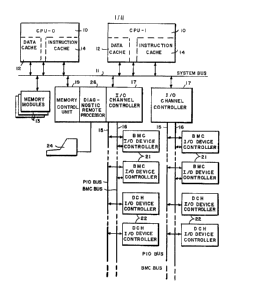
FIG. 1 uhows ~ bro~d block dl~gr~ of ~n ovor~ll uyatom
~klng UnQ of the pres~nt lnv~ntlon;
l FIG. 2 la ~ timing di~gru~ of slgn~l~ on ~ nyat~ bun of tho
¦ preaent nv-n lon
. :~
~73~17
FIG. 3 1~ n ~che~tic loglc dlagr~ of t~e bu~ ~rbltratlon
loglc of the pre~nt lnv~ntlcn found ln a requeatar of the ay~t~
o FIG. 1: ~
FIG. 4 iu ~ ~ch~tic dl~gr~n of th~ ~ddrR~s ph~ logic of
the present lnvention found in ~ requoat~r of the ~y~to~ of FIG.
l;
FIG. 5 la ~ ach~ tla di~gr~ of th~ d~t~ phc~0 logic of thu
presRnt lnventlon found ln a requester of the ~yste~ of FIG. l;
FIG. 6 la ~ ache~atlc dlagra~ of the bu~ access loglc of tho
present lnventlon of a ~e~ory ~odul~ of the ~y~te~ o FTG. 1
FIG. 7 18 ~ al~pllfled ~che~tlc dlsqra~ of th~ freez~
genQratlon loglc o~ th~ pre~Qnt lnventlon of a r~quentQr of th~
sy~te~ of FIG. 1
FIG. 8 la a acha~atic logic dlagrn~ o~ tha freozs g~nor~tion
logic of the ~e~ory control unit of FIG. l; ~nd
¦ FIGS. 9 A-l are ache~atlc loglc dlagra~a of the walt ~lgn~l
generetlon of the me~ory control unlt of FIG. 1
DETAILE~ DESCRIPTION QF THE DETAILED EMBODIMENT
An ov~rall ayate~ ualng tho tQchnlquea of tho lnventlon 1~
ahown ~n FIG. 1 wherQln one or ~orQ c~ntr~l processor unltn ~CPU)
10 ~re lnt~rconnectod vl~ ayste~ bua 11 wlth ono or ~or~ I~O
chunnel controller~ 17, a ~rory control unlt 19 and ~t l~aat one
ao~ory ~odule 13. A CPU lnclude~ a data ca~he 12 end an
lnstructlon cach~ 14. In tha pr;~orred ~nbodl~nt, thQ-o
1i~731~7
c~ch~ ~re wrlte-through cnchea E~ch c~cho ~sy h~e ~ ~4p~r~te
noed to u~0 the ay~te~ bus thua o~ch one h~ it~ own roque~t~r
loglc for g~lnlng ecc~ to the bus The I~O ch~nnol
controllers 'nter~ace wlth ~ progr~ed I~O DCH bu~ 15 nnd ~ BMC
bua 16 for th~ tr~nsfQr of d~ta to snd fro~ extern~l lnput~output
devlce B~C (burnt ~ultlplexor chennol~ controllers 21 end DCH
~d~t~ ch~nnel) I~O devlca ContrOllerB.22. The progrn~ed I~O DCH
bus 15 le ln the pro~ently preferred e~bodl~ent a~NOVA ECLIPSE
bu~ nad~ by D~t~ Generul Corpor~tion of We~tboro
M~s~chu~etts The BhC I~O d~vlce contrcllars 21 lnterf~ce wlth
both the PIO bua 15 nnd tbe BMC bu~ 16 Th~ DCH d~vlc~
controll~ra 22 are connect~d only through tne PIO bua 15 The
~e~ory control unlt 19 ~onltora tha actlvlty on th~ oy~te~ bue 11
And la r~aponslbls for correctlng any corr~ctlble error~
appe~rlng ln dutn retrlev~d ~ro~ ae~ory An op~r~tor con~ole 24
~ay be Mtt~ched to the ~y~te~ through ~ dlsgnoatlc reaote
proce~Aor 26 In th~ pre~ntly pr~ferred e~bodln~nt the ~e~ory
control unlt 19 the dlagno~tlc re~ot~ procQ~eor 26 ~nd the 1rat
lnput~output controll~r 17 ~r~ ~11 conflgurQd on the ~B~ uodul~
bo~rd The dl~gnoatic reaote proceseor 26 run~ d1~gno~tlc
routino~ ~nd intarf~ce~ with the operDtor con~ole 24
BUS PROTOCOL
In order to-provldo for ~n orderly u~e of th~ ~yat~ buo by
~11 o~ the ~odule~ nnd indlvldu~l requo~tora th~t int~rf~c~
through lt tho bua protocol o~ th- pr-a-~t lnv~ntlon sh~ll now
r~
1;~73~1~
bH deocribed wlth referenco to the tining dl~gra~ of FIG. 2. A
rQquo-ter ~y ~e a datq cach~ 12, ~n ln~tructlon cacho 1~, tho
ory control unlt 19 or ~n lnput~output channel controll~r 17
Tho lgnal~ are shown lnverted ln FIG 2 Many of the llnea are
open collector lln~o whlch loglc~lly re~ultn ln an AND functlon
belng perfor~ed on the lnputa to the 11ne Tho pro~ent
e~bodl~nt o the lnventlon wlrQ ORs slgn~lo provldad to a ayot~
bus llne ~t ~ore th~n ons lnput In order to achleve ~ wlred OR
llno wlth open collector lnputo, tbe ~lgn~l~ are ~nvort~d when
thoy are drlvnn on th~ lln~
A requ~ater lnlti~tea ~ syaton bua oporation by ~aaertlng lt~
requ~st llne (SDREOx) E~ch requsstor is ~a~lgned a dlffarent
prlorlty r~quoa~ llno Acc~s to the bu~ la r-gulot~d ln pMrt by
the prlorlty of the roquoat lln~ o~ a roquoster In FIG 2, tho
r~quea~r whlch generatea SDRE01 has prlority ovor the lower
prlorlty requestora gon~r~t1ng SDRE02, SDREO~ and SDRE~4
A ay~te~ busy llna (SDBUSY) lo provlded ln accordance wlth
tho preaent lnventlon to help provont a hlgh prlorlty requ~oter
fro~ ~onopollzlng the sy-te~ bu~ A requeoter ~ay only ~a~rt
lt~ roqu~-t llne lf th~ syate~ buay llnn lo not a~orted
How~v~r, ln ~ clock cycle wh~n th- ayste~ buoy llne 1~ not
a~-Qrted any nu~er o~ requQater~ n~y aaaert th-lr reque~t llne
to obt~ln an opportunlty to uae th~ bue In FIG ~, SDBUSY
~con~s deesa~rted ln clock cycle 2 uhich Qllowa thQ requR~tnra
whlch w~nt ~ua to -~ert th-lr r-qu-~t lln~ ln clock c~clo
I 1~73~
3. All of th~ roqu~atsr~ whlch ~a~0rted tholr requ0~t ln th~
clock cycle when th~ oysto~ bu~y llna wa- not aa~erted wlll h~v~
an opportunlty ln ord~r of prlorlty to obt~ln ~cce~ to th~
~yet~ bu~ ll. Thl~ procodure pr~v~nts a hlgh prlority ~odulo
fro~ ~onopollzing u~ of the bus. Tho h~gh prlorlty ~odulo
cnnnot ren~ert lt~ requost llno untll the ~y~te~ buay lln~ ha~
be~n dQ~sertQd. Th~ ay~t~ ~uay llne wlll re~sln ~s~rted untll
onch of thQ reque~t~ra thAt waa able to ~a~ert lts requeut h~s
flnl~hed lta oper~tlon ~nd de~aserted the ayst3~ bu~y llno. She
~yats~ bu~y lln~ of the pr~ent lnvontlon 1~ ~n opon collector
llne cnrrylng Hn lnvQrted algn~l to ~ct e~ e wlr~d OR. The
requ~t llnen ero totea pole llne~.
A requeater ~rta the ayat~ buay lln~ ~t th~ aanQ tl~
thnt 1t ~a~orts lts reque~t llnu. A requo~ter contlnuea to
es~ert the syMte~ bu~y lln~ untll any hlgher prlorlty r~qu~ter~
th~t h~ve ~l~o ~de ~ requeat ln the ffe~e clock cycl~ heve ell
co~pl~ted thelr operetlon~. nnce B r~queater h~- thn hlghQst
prlorlty, lt de~sert~ the ~ysto~ bu~y llne ~nd ~t~rt~ lt~
eddr~ phaae, sendlng ~n ~ddre~ out over th~ ~ddre~ llne- of
the ~y~tn~ bUL- Howav~r, ~y~to~ bu~y wlll re~in a~art~d lf
othar lower prlorlty reque~tor~ ~re atlll w~ltlng th-lr turn ~nd
~re th~reforQ drlvlng tho ay-te~ buay lln~. On~ clock ~ft~r
dQ~aaertlng ayatan bu-y, th~ r~queatar thR~ d~a-arta lt- r~qu~at
1 ~A~.
~ lX~3~7
~ t tho b~ginnlng o th~ addr~ss pha~o, ~ requo~tor th~t h~
obtaln~d prlorlty drlv~ tha addreaa llne- ~nd thQ con~end llne-
(SDC) of tho ey~to~ bu- and ln add~tlon drlvo~ a r~ez~ llne
(FREZ) Th~re aro thr-- co~aand llne- ln th~ pro~-ntly pref~rrQd
lnv~ntlon whlch deflno ~v~n operatlona and ~ all ~eros to
lndlcat~ no oportlon (no-op) The freaze lln~ lnforna tho
~e~ory control unlt 19 nnd tho ~e~ory voduloa 13 th~t n new
nddr~aa phasQ has b~gun T~e requaater drlvo- reez~ for only
one ~yateR clock Tho ~o~ory control unlt 19, a cQch~ or a
~a~ory ~oduln 13 ~ay ba occupled wlth othQr actlvltloa ~nd ~ay
naed to oxtend the addr-a- phaa~ to glvo 1~ ~n opportunlty to
~x~ln~ the n~w addro~4 ln a later clock p~rlod Th~ addrea~
ph~a~ 1~ extendQd whQn any ~odul~ drlve- the fraozo lln~ to k~ep
lt aa~ertQd Tha ~e~ory control unlt 19 drlvoa th- freez~ lln~
to allow data tran~fers ln progresa to co~plotQ bofore othera ~re
allowed to ~tart Tha addres~ p~ase would al~o n~d to be
ext~ndlbl~ lf lt la ln progr~aa when th- ~onory control unlt 19
la p~ror~1ng an error corr~ctlon The a~Aortlon o th- fre~e
llne prevnnta ~n ~ddres- ph~so fro~ ndlng, thu~, a tr~n~for
lnvolvlng a plurallty o dat~ tran~-rs ~ay contlnuo untll lt 1~
co~pletod In the Ca-Q of ~n orror corr~ctlon, th~ ~ddr~-a ph~o
18 ~xtendQd untll corrRctod data 1~ drivon on th- d~ta lln--
Wh~n the l~-t ~ord of dnta 1~ drlven, the ~ory control unlt
wlll dea-a-rt FREZ Tha fra-z~ lln- llk- th- ay-t-~ ~u~y lln- 1
~n op-n coll-ctor lln~
: - .', ,' ':'
~ 3~17
In tho prs~ontly pr~forred ~abodl~ont, ~ WAIT ~lgnal line in
~1AO provld~d Th~ WAIT llnQ la ~ tot~ polo llne whlch c~n only
b- ~aorted by the ~ory control untl 19~ The preaQntly
prsferr~d e~bodl~ent alao provldaa ~n Qrror llno (ERCC) by ~hlch
tho ~e~ory control unlt 19 can lnfor~ tho ao~ory of Dn error ~nd
toll the ~e~ory ~odule to got of tho bua 11 WAIT 1- not n~nt
to ~ory, lt 1~ aent to tho r~qu~t~r~ to lnfor~ th~ th~t the
d~t~ ph~nn ln b~lng prolong~d A roquo~tar c~nnot ~tart a nnw
~ddr~ss ph~ae until the p~ndlng d~ta ph~a~ h~a b~en co~pl~tod
To ~t~rt ~n ~ddrea~ phn~0 th4 fr~oz~ llno ~nd the W~IT lln~ ~u~t
bo d~-~erted or FREZ ~uat b~ un~sorted ~or two con~ecutlv~
clock~ Tha WAIT lln~ ~ay th~refore prolong a r~gue~tor'~
~ddr~as pha~o 1 Q ~e~ory dat~ error la dlsco~Qred W~IT ln
esaort~d by th~ ~noxy control unlt 19 ~t the beglnnlng o eQch
d~t~ pha-o ~nd re~lns esa~rted untll the ~ory control unlt 19
deter~lnea v~lld d~ta la ready to b~ tran~erred When d~ta 1~
put on th~ d~t~ bu~ WAIT la dean-orted unle-~ the ~e-ory control
unlt dotQct~ an error If ther- 1~ an orror, the error ~lgnal la
nas~rt~d and W~IT ron~ln~ a~sort~d untll tho corr-ct~d data 1
drl~n on tho data ~ua a~ ahown ln clock cycl-a 19 and 20 ln FIG
2 FRE2 la too alow of a ~lgnal to bo uaod to ~xtond th~
addr--a phaao whan tharo la an ~rror Th~r~for~, th~ tote~ pol~
WAIT lln- la d~alr-blo FREZ 1~ a ~low llna b~cauaa lt 18
conn-ct~d to a lnrgo nu-b~r of aodul-- for input nnd output Tho
WA~T lln- on ha o~h r n nd ~ ly d Lv-n ~V tho n ~or~ co trol
~ ' ' '
1~7311'7
u~it 19 ~nd 1~ only ~nt to tho roquoJtsr~ Tho fnwer
conn~ctlon~ ~nd lo~ r-qulrocl conductlvo Qtchlng ~kQ~ WAIT a
fn~ter ~lgnnl WAIT can b~ asa~rtQd ln r~ponse to an orror Qven
though th~ error 1~ not dl-ccverod untll l~to ln ~ cloc~ cyclo
The ~s~Qrtlon of WAIT k~opA furthQr requo~t~ra o~f the addrQ~4
llne~
If n co~putlng sy~to~ 1~ provld~d with doublo blt orror
correctlon ln the ~e~ory control unlt 19 ~8 doQs the proferrod
e~bodla~nt, thon ~ bus lnhlblt ~lgn~l ~BUSINH) ~111 be lnclud~d
~or tr~n~nlA~lon by the ~e~ory control u~lt In th~ proforrod
~bodl-~nt, a doublo blt ~rror c~n only b- corrected if there 1
~ hard orror ln tho ~e~ory ~ro~ whlch tho dnta w~ tRk~n A
double orror c~u~-d by ~ h~rd orror c~n b~ corr~cted by kno~n
~othoda ln the art by havlng th- ~odule r~spon~lblQ for tho
corroctlon ~anlpul~te th~ d~t~ ~nd do a wrlt~ back to tho ~e~ory
locatlon Double blt error corr~ctlon 18 not a part o tho
preaant lnv~ntlon ~nd ha~ been de~crlbed ln ~any text~ ~ny
~othod of double blt error corr~ctlon known to tho-~ in thQ ~rt
~ny bo usod ln con~unctlon wlth tho pro~ont lnvontlon
A bus lnhlb~t algn~l wlll C~U8Q ~ requ~ter th~t h~ drlv-n
~n addro~ on th~ ~ddr~ llnR~ to bo ro~ovod fro~ th~ ~ddroa~
11DQ8 one clock cycle aft-r the as~ortlon o tho bus lnhlblt
lln~ Th~ ~y~ta~ l- ~ad~ aw~ro tbat a double blt ~rror
corroctlon la bolng ott~pted and th~t tho bu~ la n~d~d for thot
purpo-o Upon dea~--rtlon o tho bu- lnhlblt lln~ th~t r-qu~-ter
wlll ro-Hntor th- ~ddre~ pha~o and place lt- nddr~-a b~ck out on
tho bu- Th- roquo-tor wlll ~l-o th-n ra~ rt FREZ for on~
clock ~lg 1. -10-
.
~73~1~7
If ~ ~ocond raque-ter entorn tho Dddro~- ph~eo whlle ~ flr~t
r~u~-t~r la ln itA d~t~ ph~-~ the ~e~ory control un~ t 19 wlll
~sa~rt the fr~ezQ llno as ehown ln eloek cycles 10 to 14 of FIG
2 Th~ fr~z~ lln~ la ~ert~d untll tho laat syate~ clock of
the datn ph~sQ Upon d~auaQrtlon of th- froeze llne, th- nocond
requeatQr c~n l~sdlataly ~t~rt lt- data phaae ~ the flr~t
rQqueuter enda lta dat~ ph~a~ Thla enablna n8xlnu~ utlllzatlon
of the dht~ llnea of th- y-t~ bu~ thereby provldlng a f~t~r
y~t~
In ~ ~o~ory road oper~tlon, ~anory a~ert~ 8 d~ts not r~ady
algnal ~DNREADY) untll it 1- ru~dy to place the flrst ~ddr-~ed
word on th~ sy~to~ bua Th4 ~e~ory control unlt 19 aaa~rta WAIT
a~ 800n aB the dat~ ph~s~ bogln~ ~nd ~nlnt~ln~ tho aasertlon of
WAIT uhll~ datfi 1- not re~dy a~ ~hown ln eloek eyele- 16-18 o
FIG 2 On the clock follo~lng the dQ~a~rtlon o DNREADY, tha
~e~ory eontrol unlt 19 wlll ch~ek thH data put on the bua for
error~ in a conventlon~l nann~r If an error ln found, the
n~rory control unlt contlnu-- to ~asQrt the WAIT ~lgnal An
error slgnal ~ERCC) ~111 also be ~a~rted to tell ~Q~ory to
dl~eontlnuQ drlvlng deta onto th- ~y-tQ~ bua The r~nory control
unlt 19 then h~ the opportunlty to eorrect the ~rror and drlve
eorrect~d dat~ onto th~ bu-, ~- sho~n ln clock cycloa 20 ~nd 21
W~IT la ~s~rtRd durlng tho ~ntlre corr~ctlon ph~e Upon
provldlng corr~ctQd dsta on th~ ayatea bua, th~ an~ory control
unlt wlll dn~rt W~IT Thl~ lnforaa tho roque-tQr that th~
d~ta 1- now v~lld Thua, a r-qu~-tor p~rforaing a read operatlon
aonltors tbe walt lln- ~nd ~111 not t~k~ datu froa tb- data lln~
~ntll WAIT h ~ b _ d~ rt-d
- - ~
.~
In ~ wrlte oper~tlon, or ~ ~y~tea d~ta tr~na~er fro~ one
aodul~ to onoth~r, ~ r~qu~-t~r wlll drlvo d~t~ on tho ~y~te- bua
atartln~ on th~ tralllng ed~e o~ the ~ddrea~ pha-a Deta wlll
contlnuo to b~ drl~n untll tho WAIT algnal la ds~-aQrtod by the
ue~ory control unlt DH~-ortion of WAIT lndlcAtoo th~t the
n~ory or r~c~lvlng aodule 1~ rosdy to nccopt tho roqueatQr
data If a parlty ~rror occura in a wrlto or ~yatea d~te
tr~na~or botw-on ~odul-a, ~ wrlto abort nlgnal wlll cau~o tho
ae~ory aodulo to cancol th~ oporatlon by p~rfor~lng n road
opor~tlsn lnatoad of a wrltQ Tho requaater drlvlng d~t~ on th~
bua contlnuou to drlv~ the data untll WAIT 1B do~a~rtod by ~ho
nRaory control unlt 19 Tho ~yato~ wlll hnndla tho occurrenc~ of
thla ~rror whlch 18 not correctlble a~ ~ f~tal arror
. .
BUS ARBIT~ATION
Ench roquo~ter ln tho coaputing y~toa 1- providod with logic
which ~onltora the ny-toa bua 11 and dot~ralne- wh~n that
regueatQr ha- prlorlty to control th- ayatoa bu- snd ond out
lnatructlona ~nd d~t~ ovor the bua Tho loglc of th~ prea-ntly
pr-~errod ~abodlaent for perforalng bu- arbltratlon ln ~ccord~nc~
wlth the bu~ protocol of the pro~ont lnvontlon 1~ ~hown ln Flg
3~ Whon ~ r-qua~tor wlahoa to obtain acco~ to tho ~yat~ bua,
~ 3~iLl;~7
it int~rn~lly ~rt~ tho ~gn~l SETREO ~owe~or, ln ~ccord~nce
wlth the bu~ protocol o~ th~ pr~nt lnvention, acce-~ to th~ bua
cannot b~ obtAlned unleaa th~ ~yate~ buay ~lgn~l la not
~sserted During a clock cycle ln whlch SDBUSY 1~ not ~ertod
~ny nu~ber o roquesters ~y aBaert thelr requQst llnQs If
SDBUSY 1M not ~A~erted ~nd the raque~ter w~nta to obtQln ~cceas
to tha ny~t~ buo, SETRE~ w~ a~ert AND g~te 74 ~nd
conAoquently fllp-flop 76 Fllp-flop 76 ~serts REa ln the next
clo~k cycle. REa wlll cau~e the request llne to be ~sserted Qnd
SDBUSY to be aaaerted
All requoAtera whlch h~ve na~erted thelr requeat llne durlng
thet clock perlod wlll b~ on ~ queue ln order of thelr prlority
for ~cce-slng the ayatea bu~ E~ch requeater h~s an AND g~te 72
whlch deter~lnes whether lt hes prlorlty For each requeater,
the request llne of e~ch of the hlgher prlority requester~ 18
provldod lnto ~ND g~te 72 Prlorlty 1~ ~A~erted by 8 requester
when e~ch of the hlgher prlorlty reque~ters 18 not ~nsertlng lts
requeat llne In tha pre-ently preferred e~bodl~ent, the hlghest
prlorlty requeat 18 cAu~ed by ~ refre~h cycle lnltl~ted by the
requ~t algnql REFREO Re~rnah ia a ~ethod w~ll known ln tho ~rt
for refre-hlng the cnp~cltora ~t the locatlona of ~e~ory
REU 1~ co~blned wlth ~n lntern~l drlve freez- aign~l DRVFREZ
at ~ND g~te 78 Once REa h~- been e~aerted g~te 78 wlll C~U8~
¦ REO to r~ rt-d untLi th- requ--t-r h~- prlorlty nd n~-
~:73117
ont~r~d tho addrQ~ ph~. When the roqus~t~r Hntera the ~ddre~
phase, lt as~erta D~VFREZ whlch will deMsnort gato 78 and wlll
cauA~ fllp-flop 76 to doas~ort th~ request llno at the next
clock. DRVFREZ 18 ~l~o provld~d to g~te 80 whlch wlll
lnaRdlat~ly dea~ert tho aystQ~ busy 11ne. Tho gener~tlon ~nd
uao of DRVFREZ ln the ~ddre~s phsa~ i~ dl~cuehod ln tho aectlon
on ~ddrQsn pha~o loglc bolow.
Thore ar~ cert~ln sltuatlons ln whlch a requQater wlll need
the bu8 for ~n extQnd~d pQrlod o tl~ b~c~us~ of ~ hlgh prlorlty
lnstructlon whlch requlres the co~pletlon of ~ number of
lnatructlon~. A ae~aphore la an exa~pl- of auch an extended
lnatruction. Under theae clrcu~atunces ln whlch an extended uae
of tho bus 1~ roquir~d a requeater ~aa~rt~ the algnal SETLOCK.
SETLOCK 1~ co~blned wlth A SETR slgnal ot AND g~ts 81. SETR ~a
~sserted by OR goto 82 when ~ reque~ter 18 p0rnltted to asa~rt
lts reque~t llne. A co~bln~tlon o SETLOCX ~nd SETR wlll os~ert
BUSLOCK through gate 81 and fllp flop 8~. At the co~pletlon o
one opor~tlon ln a serl~a requlred or n sQ~aphore, SDBUSY wlll
not b~ da~s~ertad ~a u~ual bocausQ of BUSLOCK nt OR gate 86.
Thernfore, SDBUSY wlll r~ln anaortod ~nd thq co~bln~tlon o
BUSLOCK, PRIORITY ~nd SET REC at AND gate 88 wlll cnu~e the
r~que-t llnR to ren~ln naa~rted or tho next operatlon ln the
~on~phore. A bu~ lockod ~at of ln~tructlona ~ay be lnterrupted
by 9 hlghor prlorlty r~queat auch n~ REFREa. The presontly
~X7;~
do~crlbod ~yate~ g~vo~ REFREa the hlgho~t priorlty ~nd ~llowa
~rtlon o~ REFREa e~n durlng ~n SDBUSY. Thus, ater ~ach
op~r~tlon lt 1~ n~ceassry to check for prlorlty even though
prlorlty ~xi4tod ~t th~ boglnning o~ the ~phor~. In the l~ct
operation o~ ~ bua lock~d ~quence, SETLOCK wlll no longer be
R~aerted ~o when SET R la aaaQrted, thR co~bln~tlon o BUSLOCK
and not SETR at gQte 81 wlll cRuao aUSLOCK to bR res~t. The
reaot occurs wh~n the laat operatlon haa prlorlty to proceed a8
det~r~ln~d ln g~ta 88 whlch a8Aert8 SETR. Henceforth, th~a laBt
op~ratlon wlll be h~ndled ln a nor~l ~nnner.
ADDRESS PHASE LOGIC
Oncs ~ r0qu~ater d~ter~lne~ lt hn~ obt~inod priority ~or
~cceaslng the syste~ bus, lt nay than go lnto lts addreas phaae.
The ~ddross phsse loglc for a requeater 1A ~hown ln FIG. 4. The
~ddr~- ph~aQ la entered ~u ~hown ~t co~blnstlon g~te 94. Two o~
tho requlrnaonta ~or co~nenclng an sddress ph~ae are that the
r~queater la aasertlng a raquQ-t aa lndlc~t~d by REO and th~
requeater hna prlorlty both o whlch were deter~lned ln the bua
~rbltratlon loglc. It 18 alao necea~Jry to check th~t the ~reoz~
slgn~l tFREZ) la not belng saaertRd alncQ eny ~odule can aaaert
the FREZ algnal over th~ yato~ bua to nxtend the preYlous
nddre~ phaM~. ~ reque~ter nay not ~tart lta addre~ phaa~ untll
th- pro~iou~ requo~tor h~ co~pl~ted lt~ ~ddro~ pha~e. When ~n
addreaa phna- 1~ co~plet~d ~ dat; ph~e wlll l~edlstely
~ ;~73117
co~once Thersfor~, ln ~ddltion to the frnezo sign~l, the WAIT
~lgnRl 1~ a crlterlon for startlng ~n addree~ phaao. An ~ddress
ph~se can begln lf both WAIT ~nd FRE2 ere deassQrted If WAIT
w~ra ~tlll ~s~erted, lt would ~ean that the d~ta pha~e 1~ bolng
extended to perfor~ ~n error correctlon or block tr~nsfer It 1
~lao po~albl~ to start e new eddre~ ph~se lf the freoze slgnal
~nd a fr~ze anvo nlgn~l ~FREZSV) both ~ro not aaaerted The
fro~ze ~ave lgn41 la ~ one clock delayed veralon of the frsez~
ffl9n~l produced ln fl1p flop 91 The co~blnAtlon includlng the
freeze ~ave 41gn~1 would per~lt ~n addreaa phaae to b~gln ln a
altu~tlon ~uch e~ th~t ~t clock cycla 8 of FIG 2 where WAIT we~
a~erted ln a ~econd dnt~ phas~ of a block transfer but no
addre-~ ph~o was ln progr~s~
Upon ~eoting th- condltlon~ for beglnning ~n ~ddreaa phs~e,
fllp-flop 92 causea tho aa~rtlon of a drlve addr~sa slgnal
(DRVSA) end 11p-flop 94 cau~ea the aaaertlon of DRVFREZ The
DRVFREZ slgnal la uaed by the bu~ ~rbltrntlon loglc of FIG 3 to
deasaert SDBUSY Whon th- requeater ~aerta DRVFREZ, gate 96
wlll nor~nlly ~a~rt FREZ FREZ wlll be fed back lnto gate 90
~nd thu~ tho fllp-flop 94 wlll reaet DRVFREZ Thus, ~ requeater
only drlves th~ freez~ algnal for th~ flrat clock cycle of an
addrea- pha-a Th~ DRVSA ~lgnal, however, whlch la c4ualng the
~ddre-- llneA to be drlven by th- r~quo-ter wlll contlnue to ~e
a-a~rtod lf FREZ 1- drlven by ~o~- other ~odul~ or lf WAIT 1-
~ertod FREZ can be drlvon by ~ ~odule whlch ne~da ~ore tl~
b-ore r--dlng th- ddre~a lln--i If ~n ln~Lructlon 1- p-ndlng
1~73~
whll~ a n~w ~ddr~n~ ph~ la belng requ~st~d, the ~nory control
unlt wlll ~aaart FREZ untll the la-t d~ta word 1~ tranaferr~d
However, lf th~r~ 18 ~n error on th~ laat data tr~naer, slnc~
FREZ la alowor to re~pond to ~n ~rror thsn WAIT, lt b~co~ea
nace-anry to chec~ the WAIT ~ignsl befor~ dlscontlnulng to drlve
the addros~ algn~la on the addrQsa llnea Th~reore, ~n addre~a
phase 1~ not co~pletQd untll both FREZ and WAIT ere d~aaserted
Th~ bu~ lnhlblt algnal ~BUSINH) 1A ~ signal whlch ~y be
provld~d ln n ay~te~ to h~lp l~ple~ent double blt error
correctlon The bua lnhlblt nlgn~l la provlded to return ~
roqueater ln the ~lddle of lt~ ~ddr~sa phaa~ back to the polnt
when lt wa~ about to co~ence its addre~a phaa~ Bu~ lnhlblt
c-ua~a tho requeater to Mtop drlvlng slgn~l~ on the ~ddres~ and
co~aand llnea Thua, the r~que-ter la ta~en off th~ yate~ bua
Tho rQqu~ater wlll be abla to regaln acceaa to the ayste~ bus and¦
re-tart lta operatlon at th~ co~pletlon of the double blt error
corr~ctlon and deaaa~rtlon o the bua lnhlblt ~lgnal Tbe bua
lnhlblt ~lgnal la aaved to provlda a one clock delQyed veralon,
USINHFF ln ~llp ~lop 93 The sved bu~ lnhlblt slgn~l ln
conbln~tlon wlth DRVSA at gato 90, a~ta fllp flop 92 and fllp
~lop 94 Thua, the requeat~r 1- ready to ssaurt DRVSA and
DRVFREZ, th- clock ~ftHr th~ bua lnhlblt ~lgn~ de~-aertad
Tho d~aa~rtlon of bua lnhlblt la fed lnto gat~ 96 ~nd 9atR 98 to
n~b~o FREZ and th- ~ddroa~ lln~-
-17-
~X731~
R~Q~E~T~ TA PH~E
¦ A r~que~t~r beylnn ita d~ta ph~se l~odl4t~1y upon co~pletlng
lt~ nddrnas ph~-e Tho data phase ah~ll bo,do-crlbod wlth
rRf~rQnc~ to FIG 5 Thla can be al~ply det~r~lned by feeding
thH drlvo addreas algnQl, DRVSA, lnto a data pha~e Atat~ ~achlne
100 Upon dQasaertlon of DRVSA, the d~ta phn~o nt~te ~achine lOO
enables th~ data lln~ drlvora lf tho co~Hnd ~o dotor~lned by
algn~la 5DC 0-2 fro~ the co~and llne~ lnvolvQd ~ wrlto
speratlon If tho co~nd lnvolv~a n re~d thon dnt~ la t~k~n off
th~ data llne~ lnto n d~ta lnput roglstor 102
A d~ta ph4ae la not conpleted untll the do~a-~rtlon of the
walt algnRl Ther~or~, WAIT la lnput lnto thR drlve ph~e state
~achlne 100 When WAIT la ~oaorted the d~ta llno drlvera r~Aln
onnbled or the data ls not t~ken o~ the d~ta llnea lnto th~ d~ta
j lnput regiator d~pendlng upon the lna~ruction whlch 18 pendlng
,1 In ~ wrlt~ operatlon otor the d~aaaertlon o WAIT tho dota llne
drlvers ~ro ahut o~ For a read operatlon, th~ deaasertlon o~
WAIT cau-oa the data, whlch ~u-t now bQ valld, to be taken off
tho date llnes and into tho dnt~ lnput rogioter 102
EMORY ~ODULE
Re~rrlng no~ to Fig 6, ~ oi~plified ~cho~tlc of ~ ~e~ory
~odul~'a bu- acce-o loglc 1- llluatrated An addre~a docoder 120
roc~lvQa tho co~and aign~la (SDC~ snd tbe neceaa~ry ~ddresa
~9 al (5A~ o~ th ~ t- d-c-r~ln- ~ ~h-r thl-
particul~r ~o~ory ~odulo h~a boen ~ ct~d by tho operstion
p~nding on th~ ~ysto~ bua. S~lectlon of the ~e~ory modules
d~pend~ on wh~th~r th~ ~o~and 18 8 ~ory lnstructlon and 1 ~o
wheth~r tho ~e~ory ~odul~ 1~ th~ one ~ddreaa~d. If the ~odule 18
~el-ctnd, ~ bonrd sel~ct lgnnl 1~ ~ssertQd. At the beglnnlng of
n d~t~ ph~a~ na doter~lned by ~ d~t~ ph~a~ decoder 122, flip-flop
124 annert~ ~EMACK lf bo~rd select la ~aortod. Th~ d~ta ph~e
decoder 122 deter~lnea th~t the dnta ph~ao la beglnnlng by
obt~lnlng fro~ ~n ~ddress ph~-e d~coder 12~ wh~n th~ 4ddress
phaao ends. An ~ddrRa- ph~s~ enda when FREZ 1~ not uaaerted and
the error 11ne (ERCC) la not ~s~rted. Tho d~t~ ph~ao co~aencea
l~medlat~ly followlng the end of the Qddr~aa pha~e.
If tha ~o~ory ~odule has beQn a~l~ct~d, 1~ 1A l~port~nt th~t
the ~ory ~odule have Gn opportunlty to t~k~ the full addre~
off th~ ay~ten bu~ for lts uae ln peror~1ng the preacrlbed
op~ratlon. In order to kQep tha address on the 4ddreas llne~,
th~ ~e~ory ~odulu of tha pr~nont lnventlon c~n ~a~rt FREZ. The
FREZ slgnAl prolongs th~ nddr~as ph4sQ of n requeater. ThR
~eAory ~odul~ lncluda- e r~d~wrlte` control 128 whlch generatea
algn41 lf thQ ~ddrQaa latch 1~2 la ~ull ~nd 18 unable to eccept
thH ~ddrasA on the syat~ bua at thn pr-Aent tl~R. A FRE2
control 130 gQnarDte~ tha FREZ ~lgnnl lf the addresa latch la
~ull~ end th- n-eory Aodule ha- been selected. FREZ la generated
aft~r th- addr~-- pha~o haa be-n ~ntered ~nd after tho 1rat
clock cycl~ of tho ~ddre-~ phJ-e. For th- ~lrat clock cyclo of
th~ eddroJ~ phJa~, tho roquo~ter la genaratlng the FREZ algnnl.
~ 3LX73~1~
Th~ re~d~wrlte control reco~vo~ ~ w~te ~bort ~lgnnl
(WRTABORT) whlch 1~ uaoful in n double blt rror correctlon. I
~ ~yate~ lncludQs doublQ blt Rrror corroctlon, lt 1~ de~lrnble
thnt the ~-~ory ~odulo b~ ~ble to ~bort ~ wrlte ~nd re-tart lt
lnter ~ter th~ douhle blt error correctlon hn~ bQQn coapleted.
Th~ wrlt~ bort slgn~ y ~180 bo usQd whan there 18 ~n nddres~
parlty error to pr~nt a wrlte lnto tho wrong nddrQsa. Al~o
u~sd ln the doubl~ blt error corr~ctlon la th~ ERCC algn~l which
toll4 ~ rQ~d~wrltQ control 128 to ~top sequenclng through lt~
a~ory ~rray ~nd got off the bus. Tho ro~d~wrlt~ control 128
control~ the ~ddre~slng of tha ~e~ory ln con~unctlon wlth th~
Qddre~s lntch 132.
The re~d~wrlte control 128 1~ the sourco of the dt~ not
recdy slqn~l ~DNREADY) whlch wlll b~ la~ued upon co~encaa~nt of
the d~t~ ph~a~ when the neaory ~odule 1~ selectRd for ~ re~d
unlees th~ ~odule haa the ~ddresaed dat~ rendy to drlvo on thQ
d~t~ llne~. When d~t~ not re~dy h~ been Hsa~rted, lt wlll be
doQs-ert~d aftor th~ ~e~ory aodul~ ~cce~ae~ the reque~ted d~ta
fro~ RA~ 134 ~long wlth the d~t~'~ a~ocloted check blt- (CBIT)
for arror detoctlon and corroctlon. A d~tQ lnput r~glator 1~
provlded for t~klng data ~nd check blts off of ~ bua ~nd holdlng
the~ table for two clock~ untll th~y ~ro urltt~n lnto th- ~a~ory
13~ durlng ~ wrlto op~r~tlon. In tho pre~ntly preferred
e~bodlaQnt, ~enory 134 1- ~ dynaaic RA~ o~ 264K. Howover, the
ln~ntlon a~y b- pr~ctlced wlth ~ny typ~ or Bl Ze of ~e~ory.
Ind~ad, th- bU~ protocol of tha pr~ont lnv~ntlon ~dvunt~g-ou-ly
provlda- flQxlblllty to ~llow ~ ~10WQr ~ory ~lnco FREZ c~n b~
g~n-rat~d to prolong tho addr~-~ phn-- nnd D~READY c~n oxtond the
datn pba- on tho sy~to~ bua.
-20-
.
I ~ L17
REOUEST~R_LOGIC F0~ ~RIVI~G_~REEZE
Accordlng to th~ dlstrlbut~d control over tho reoze elgnal
of the presHnt lnv~ntlon, an ln-tructlon cqch~ 14 and a data
~achæ 12 ~ny g~nsrate FREZ to delay an addre-s phaA~ lf thH cache
c~nnot pr~aontly do lts lnv~lld~tlon procodure on the new
~ddrQas It 18 well known ln th~ art to provld~ wrlte through
c~ches wlth ~ ~ech~nl~ for lnv~lld~tlng d~ts lt ha~ ntored lf
tho correspondlng ~o~ory locatlon la belng written lnto
Roferrln~ now to FIG 7, sn lnvnlldntlon ~t~te ~chlne 140 18
provld~d to control th~ lnv~lldQtlon proc~dure An uddreaa l~tch
142 t~ko~ ~n Addr~s o~ tho syate~ ~u~ lf the op~ratlon l~ ~
writo a~ deter~lned by th~ co~and blta t~ken of the bua by the
lnv~lldstlon t~to rachlne 140 A teg ~torn 146 cont~ln~ ~ tag
or each storage locatlon ln the cach~ The tag lndlcate~ whlch
pag~ ln ~ ~e~ory ~odule the d~ta ln thQ cach~ wes tokQn fro~ An
sddr~na co~psretor 144 deter~ln~s whether the addresaed ~e~ory
locatlon corre~ponds to eny o the page Rd d rOB80B ln the t~g
~tore ~ valldlty blt storQ 148 cont~lns a blt or e~ch stor~ge ¦
locatlon ln cache to lndlcatR wh~ther the data stor~d ln c~ch~
re~alna velld If a wrlt~ l~ p~ror~ed on n ~enory loc~tlon
corre-pondlng to o cach~ ator~ge loc~tlon, the v~lldlty blt for
th~ c~cho stor~go loc~tlon wlll b~ aada lnvalld
In ~ccordance wlth thQ pro-ent lnv~ntlon, ln a sltuRt~on ln
whlch ~ddroa~ lstch 142 la ull when a n~w wrlto opor~tlon 18
drlv-n on ths addr~ bua, tho c~cho g-nerato- FREZ to prolong
th~ ddr-a~ p untll t~ c-ch c~n t~k- th~ ddrea- lnto lta
. ~ 3~
l~tch 142 to co~plote lta ln~lid~tlon procsduro. Th~
ln~nlld~tlon st~to ~achln~ 140 c~n gonerata FREZ undor theAe
condltlons ualng Mny approprla~e loglc gatoa deter~lnable by one
of ordlnary aklll ln thQ pertlnent art.
FREEZE SIGNAL GENERATION BY THE MEMORY CONT~OL UNIT
Reforrlng now to Flg. 8, the loglc wlthln ~ ne~ory control
unit for the g~neratlon o FREZ 18 llluatrated. huch of th~
loglc ehown refera to the generutlon of FREZ durlng ~ dou~le blt
error correctlon. Slnco the double blt error correctlon 1~ not a
p~rt of the presont lnventlon, thla loglc wlll not be descr1bed
furth~r herein. It la aufflclent to atRte that the ~e~ory
control unlt 19 c~n genarate FREZ whQnever n~c~ffaary durlng
double blt ~rror corr~ctlon by ~aklng FREZ d~pond~nt on the
~pproprlate algnal~. FREZ 1~ alao genernted by a ~e~ory control
unlt ln order to perfor~ a snlff opQrstlon. Snlf la peror~ed
by the ~a~ory control unlt 19 to detect and corroct errora ln
ne~ory locat~on- whlch n~y have occurred ~a a re-ult of an alpha ¦
p~rtlcle hlt. The slgn~l FREZFF 1~ gener~tod a~ a re~ult of
approprl~te algnal~ lndlc~tlng a doublo blt ~rror corroctlon or n
snlf op-r~tlon.
no~ory control unit 19 ls re~ponsible for genoratlng FREZ
whHn ~n ~ddroaa phaaQ 18 bogun durlng a prolongod d~t~ phas-
cau~ed by a block lnatructlon for ln~t~nce, ~ block read la ahown
r~queatod by th~ thlrd requQater ln FIG. 2. Gato lSO dat~r~ln~a
p~
¦ th~t lt hQ~ not ~t~rt~d g~ner~tlng FREZ yet through 1ip flop
¦ 15a, nnd elther dat~ 1~ not re~dy or thsre la no ~ory ~t th~
¦ loc~tlon ~ddre~aed (EXTEND) or there 1~ ~ block trnnaer wlth
l ~ore th~n one d~ta word re~lnlng to be tr~n~erred ~8 lndlc~ted
¦ by not ZEROCNT Th~ FREZ co~and wlll at~y gen~r~t~d on the bua
through g~te lS2 na long ~a th~ pendlng co~nd 152 r~ln~ v~lld
and untll the d~ ~ 18 re~dy, the block tr~nsf~r re~ch~s tho l~t
word (ZEROCNT M~aerted) or EXTEND 1B de~aaerted dependlng on
whlch of theGe c~uaed the FREZ Slnce lt 1~ pos~lbl~ for ~
requenter to abort an lnatructlon by alterlng lta drlvera to
dr~ve ~ no-op r~th~r th~n the co~nd th~t waa orlglnnlly drlv~n,
lt 18 dealr~ble ~or the ~ory control unlt to check whether
th~r~ v~lld co~n~nd on tho lln~ ~o ~a not to tl~ up tho
addr~sa llne~ wlth ~ no-op or nn lnv~lld lnstructlon An
inatructlon abort nlght occur ~n n altu~tlon where d~tQ ceche 1~
belng ~ddre~aed but lt la lesrned th~t the ~e~ory ln the c~che la
no longar ~ vslld repreaRnt~tlon of whQt exlata ln the ~ctual
l ~e~ory The reque~ter whlch ntte~pted thla ahort cut o a~oklng
¦ ~e~ory ro~ th~ c~che rathQr th~n d~rectly fro~ ~e~ory ~borts lt~
lnatructlon because the rQqu~atQr doe~ not h~v~ euf1clent tl~e
to refor~ulste th~ ln~tructlon to ~ek th~ dst~ ro~ tha ~nory
r~ther than tho c~ch~
Generntlon o FREZ by the ~orory control unlt mu~t ~l~o occur
to cover thQ ltustlon whorR ~n error correctlon occur~ on the
l~at trQn~er of a word ln ~ block tr~na~or o ~ nu~ber o~ word~
ln ~ d~tn ph~- FRE2 la d-~-a~rtQd at thQ la-t d~ta word ~nd la
:' ~ ' ' ', ' . ~' ,'
- ~
'
~'73~
thu~ d-c~qrted whlle th~ correction 18 bolng ~ade ~nd the
corrected word 1~ belng placod on the syate~ bu~ by the ~e~ory
control unlt. Thua, lt ~y be po~albl~ for ~nother ~odule to
~tart lt~ ~ddreas ph~ae ~ec~u~ o two cons~cutl~e clock cycles
wlthout ~ FREZ. To prev~nt ~uch nn occurrence the ~e~ory control
unlt generstes FRE2 through g~te 154. G~t~ 154 w111 ceu~e F~EZ
to be g~n~rated lf th~ Qrror slgn~l 1~ ssaQrtedJ th~ error slgnM1
wn~ not ~saerted ln the 1ast clock cycl~ (ERCSV) ~nd there la
v~lld co~nd on tho ay~ten bus or FREZ 18 ~aerted on th~ bu~.
G~te 156 hnndle~ doubl~ blt error ~ltu-tlon.
GENERATION OF WAIT SIGNAL BY ~E~ORY CONTROL UNIT
The WAIT slgn~l 18 aa~rted by the ne~ory control unlt 19 ~t
the beglnnlng of a d~t~ ph~o and re~alns ~aaerted untll th~ d~ta
placed on the d~t~ llnes la deter~lnQd to be valld ~nd correct.
If a co~and 18 pasalng ~ block of word~ of d~ta, WAIT 1~
deasaerted cfter e~ch data word 18 v~lidly tr~nsferrod over the
ay~ten bua. WAIT la re~aaerted when the dat~ llnes are prep~red
to co~nca tr~naer o th~ next word of dat~. Th~ loglc used ln
th~ preaently pref~rrQd erbodlaent of the ~-ory control unlt for
gener~tlnq WAI T la ahown ln FIGS. 9 A-I.
1r~t co~ponent o th~ WAIT algn~ a load count algn~l
~LDCNT), genQrated n~ ahown ln FIG 9A. The lo~d count algnal
lndlcat~ that tho ~yat~a la ~lth~r at th~ beglnnlng of ~ d~te
ph~an or th~ bua 1~ idl~. The lo~d count algnal la aaserted lf
th- y-t-~ 1 not ln the ~Iddln of a d-t~ pha.- <ZEROCNT~, th~
.
1.~7;31~7
¦ ~ddreaa ph~a~ ia not b~ing ~xtnnded by a FREZ ~lgnal, th~ nyate~
¦ la not ln the ~lddle of ~ double blt error correctlon cycle
l (DBEC) Mnd the last d~t~ pha~e h~a been co~plQted (not WAIT). If
¦ th~ count ia other than zero then the ay~tem la ln the ~lddle of
¦ ~ bloc~ tr~nafer lnvolvlng morn than one d~ta word ~nd thu~ w~
are in the middle of n d~ta phsaQ. The dstn phase wlll not
begln unt~l FREZ haa b~en deasserted, thus lo~d count wlll not be
nsserted while F~EZ ia asaerted. DBEC i8 a s1gnal whlch
lndlc~tes th~t a double blt error correction la t~klng pl~ce.
The detalla of handllng double bit error correction for~s no part
of the pre~ent lnventlon, except to the axtent th~t the ~y~tem of
the present inventlon provldea ~ protocol whlch can mnke
~llowancea for the delQys c~used by double blt error correctlon.
If WAIT la preaently being ~sserted, the preaent dat~ ph~e h~s
not yet been completed. A n~w dQt~ ph~se c~nnot begln untll the
old d~ta phaae h~s been completed aB lndlc~ted by the de~a~ertlon
of WAIT.
¦ Since the lo~d count signQl ia uaed to lndlc~te the beglnning
of a dat~ phuse, lt 18 ~180 used to loMd the counter whlch la
used when ~n lnatruction auch ~8 a block lnatructlon requlrea the
tranafer of more th~n one word o data. Load count i8 nlao uaed
¦ ~8 ~ crlterla for ~ flrat d~tQ slgnal (FSTDATA).
¦ The preaently preferred enbodlment providea for elght
I com~nda whlch ~re cod~d lnto three command bltR, SDC0, SDCl ~nd
¦ SDC2. Referrlng now to FIG. 9B, lt 18 dealr~ble to ~v~ th~
l comrsnd durlng the dQt~ ph~se ~n addltlon to no~ Qddreaa bita
¦ whlch wlll be u~eful ~t the completlon of the datQ pha~Q. A 8~VQ
clock ignAl SVCLK~ 1~ g-n-r-t-d whleh r-r-ln~ rt-d dDrlng
- , .
- ' . ~ ' '
,
'' '
' '
- :
':
~73~17
th~ dnta pha~. A~ ~hown at 1atCh 160, SVCLK beco~e~ ~as~rted in
synchronlzntlon wlth th~ syste~ clock (SYSCLK) when there i 8 a
lo~d count ~ignal a~erted. The latch 160 al~o preven the
as~ertlon o~ SVCLK when there 1B ~ double blt error correction ~a
lndlcatQd by the slgn~l BDBEC. The SVCLK algnMl 18 used ln l~tch
162 tO 8ave an approprlate addre~ slgnal throughout the dat~
phe~e. In the preferred e~bodi~ent, address slgnal SA 31 1~
~v~d as ~lgnal SA315V. ~ddltlonally, ~ll o the co~nd blts
are ~aved ln l~tches 164, 166 and 168.
The co~and slgnals are used ln con~unctlon wlth the lo~d
count ~lgnal to load th~ counter ns shown ln Flg. 9C. The
counter ln the preferred e~bodi~ent 18 two blts, the mo~t
slgnlflc~nt blt CNTBIT0 and the leaat slgnlf~cant blt CNTBITl. A
syste~ havlng block operatlons whlch lnvolve the tranafer of more
th~n four words would requlre further blts ln the~r counter. The
loglc gatea 170 ~nd 172 decode the ln~tructlons lndlcated by
LSDC0, LSDCl and BLK. BLK la generated fro~ the co~and algnals
to lndlcate whether there la a block tr~n~f~r. When the load
count ~lgnol la ~aaerted, each blt of the counter can be loaded
wlth lta correct value through fllp flop 174 ~nd fllp flop 176.
The counter wlll lndlc~te the nu~ber of words ln A transfer ~lnu~
one.
The counter of th~ pre~ent lnventlon la not ~ wrAp nround
counter. In other words, lf the counter 1~ decre~ented to zero
lt wlll re~aln at z~ro lf an atte pt la m~do to decrement lt
~ ~731.17
further. At tho compl0tion of th~ d~t~ tr~n~fer of ~ch word in
~ block or partl~l wrlte lnstructlon, the counter wlll be
decrenented. ThR decre~ent count ~lgnal DEC-CNT la gener~ted ln
gate 178. The counter i8 decre~ented ~t the beglnnlng o the
tr~nsfer o a ~ord of d~t~ durlng the datQ phaao. A FORCE WAIT
slgnal 1~ generated at the beglnnlng of th~ tr~n~fer of e~ch word
o~ dat~. FORCE WAIS la gener~tRd regardle~a o~ errors ln the
data. I~ the me~ory control unlt detect~ an error ln the dats on
the syste~ bu~, lt wlll contlnue to aAaert WAIT and make a
correctlon ln the datQ BO that corrected data can b~ pro~ided ~or
th~ ~yste~ bus. The ne~ory control unlt wlll nasert an error
slgnal ERCC when lt hca detected an error ~nd 1~ ln the process
o correctlng th~t error. Thereore, at the co~pletlon of FO~CE
WAIT lf there 1~ no error, tho counter wlll ba decre~ented ln
reaponae to DE~-CNT. The counter 18 not decrenented lf there 1~
~n error slgn~l ERCC ~sserted. G~te~ 179-182 lndlcate tha u~e o
thQ decre~ent count algnal to decre~ent the counter.
GatQ 184 of Flg. 9D 18 used to generate ANYSDC whlch
lndlcates th~t thera 1~ ~ valld conn~nd belng lasued over the
con~and llne~ o~ tho syHten bus. When all o~ the co~and blta
are z~ro, a no-op 18 lndlcated. Gate 186 18 used to generate a
zero count sl~nal ZEROCNT whlch lndlc~tea when tha count~r i8 ~t
zero.
,
,
.
~27~7
Ref~rring now to Fig. 9E, ~llp-flop 188 1~ provlded for
gener~tlng the algnalo flrat d~t~ (FSTDATA) ~nd lutch~d flr~t
d~ta (LFSTDATA). The flrat data 8t gn~ls are naserted whon the
load count algn~l 1~ ~snertacl nnd there 1~ ~ volld co~nd on th~
co~and llnea. A~ lndlcatQd above, LDCNT lndlcate~ that lt 1B
~lth~r the beglnnlng of ~ duts ph~Ae or the bus 1~ ldle. The
ANYSDC nlgnQl lndicates that there 18 a valld co~and on the
sy~te~ bus. Thereore the co~bln~tion o these ~ignnla lndlcate~
the co~ence~ent of the data pha~e.
Latch 190 provldes n saved vernlon of a p~ge lnhlblt algn~l.
The p~ge inhlblt ~lgn~l ~PAGEINH) 1~ l~sued by a a~ory ~odul~
when b~d ~emory, me~ory th~t haa f~lled, 1~ boing addre~sed.
Thls 1~ n featur~ of the pre~ently pref~rrRd e~bodl~nt of the
lnventlon ~hlch 1~ not nQcQssary to the lnventlon. However, lt
ln a u~eful feuture for avoldlng unnec~sssry operatlona on ~e~ory
whlch la no longer ln U~Q. For exa~ple, REFRESH and SNIFF
oper-tlona which nre nor~ally carrled out over ~n entlre ~e~ory
wlll be warned by the pnge lnhlblt ~lgnal that there 1~ bad
~ory ~nd th~t they c~n aklp that page of ~ory. L~tch 192
provlde~ ~ s~v~d ver~lon of MEMACK. MEMACK 1~ al~o ~ slgnal
provldod by ~ me~ory ~odule a~ dlscu~sed ~bove. It 18 ~n
acknowledgenont algnal fro~ the ~e~ory ~odul~ that n vnlld
locatlon ln ~e~ory hno boen addreAoed.
Reforrlng to FIG. 9F, an ext~nd algnal 1~ lncluded aa an
addltlon~l featuro of th~ pre-~ntly de~crlb~d ~y~to~ to handle
~ltu~t10n- l hLch th-r- 1- no v lld ~e~ory ~dre~ ln a read
~ 73~7
op~r~tion. Such ~ read fro~ ~e~ory would c~u~e ~n i~di~te
provl~lon o zeroa over the d~t~ llnea. Tho I~O ch~nnel
controllern 17 would be un~ble to hAndle the r~pid ~upply of
theae zQros over the d~ta channel ~nd they have no w~y of
~bortlng the read befor~ thQ zeroa ~rQ sQnt. Slnce the ~ddreas
loc~tlon ln ~emory 18 not v~lld the ~e~ory ~odule wlll not
provlde ~ d~t~ not resdy slgn~l ~DNREADY). Thereforo, th~ extend
slgn~l subatltutea for the d~ts not ready slgnal to prevont the
ne~ory ~odule fro~ proceedlng fn~ter th~n the I~O ch~nnel
controllQr cun h~ndle. The algnal EXT 18 aaserted ln gote 194
when there 1~ ~ re~d ro~ ~e~ory, ~nd lt la thQ flr~t clock
slgnQl of a re~d dat~ ph~ae. EXT la co~blned wlth not MEMACK
whlch lndlc~tea th~t no v~lld locQtlon ln ~eaory h~a been
addresaed. In such ~ c~ae the uo~ory nodule w117 bé pro~ldlng
zeroa over the dat~ llnes. Thua, when there 1~ ~ read operstlon
of ~n lnvalld ~e~ory locatlon, the EXTEND slgn~l wlll ~e
~s~Qrtad by 11p flop 196.
Referrlng now to FIG. 9G, the goner~tlon of ~ FORCE WAIT
~lgnAl le llluatrMted. A fllp~flop 198 wlll cau~e FORCE WAIT to
be A~-erted whene~r the d~ta ph~se ~t~rts na lndlc~ted ~y the
uignnl LFSTDATA. FORCE WAIT i8 fed b~ck into n nultlpl~xor 200
ln order to toggle betuQen two crlt~rl~ cholcea ~ter the flrst
clock cycl~ of the dutA phaaQ. When FORCE WAIT h4a ~een ~aerted
the ~ultlplexor lookff ~t wh~th~r the d~t~ 1~ ro~dy and wh~ther
there 18 ~n extend algn~l o~aertQd. FORCE ~AIT wlll r~in
~ ~2733~17
¦ ~s~erted untll the dat~ la r~dy ~nd the extend ~ign~l la
¦ de~aa~rted. Once d~t~ 1~ rendy, WAIT wlll no longor be forcod
¦ but will b~co~e condltlonal upon whether there 1A ~n error ln the
¦ dat~. Thus, when DNRE~DY ~nd EXTEND are not n~aarted, FORCE WAIT
¦ wlll heco~Q dess~rted. Whlle deasaerted, the ~ultlplexor wlll
¦ focua on the COUntQr. If th~ countor la ~t z~ro, FORCE WAIT wlll
¦ r~aln un~erted. Howover, lf th~r~ srQ ~ore word~ to be
tr~naferred ln thla data ph~a~, th~ FORCE WAIT slgnnl ah~ll be
l reas4~rted.
¦ The lnltlntlon o test proceduren ln ths ~ory control unlt
~re provld~d for ~a ahown in Fig 9H. Wh~n FORCE W~IT ia n~aerted
and dutA i~ roady, fllp~flop 202 wlll CaU8~ the nasertlon of
¦ TESTFF. The TESTFF ~lgnal lndlcatea to the ae~ory control unlt
¦ the proper tl~o to p~rfor~ lt~ error testa on the ~e~ory
tranaferred ov~r the ayateR bua. The teata arn peror~ed aa aoon
a~ the d~ta beco~es re~dy.
l Th~ slgn~l MEMTEST ia uaod only when dat~ 1~ b~ing re~oved
¦ ro~ ~o~ory. Thu~, gatea 203-205 whlch deter~ino MEMTEST wlll
¦ decode the co~n~nd ~ign~la to ldentlfy wh-thor thore i4 n ro~d
fro~ ~e~ory in~truction. In ~ co~plox oporatlon ~uch ~ a read
nodl1ed wrlte, a MEMTEST wlll only be perfor~ed on the ~cond
word of tha d~ta ph~a~, that belng tbe word whlch la t~kon froa
~emory. A tost of tho ~e~ory will not b~ conductod lf thoro la
no ~lld no~ory loc~tlon addrQ~d by th~ pendlng ln~tructlon.
Ther~foro, MEM~CKSV 1~ lnput lnto g~t~ 205. Alao, u~ do not u~o
tho MEMTEST whon thar~ la a page inhlblt whlch l~dlcat-~ th~t
dRad ~ory hna b-~n nddre--ad. Nor 1- th~r- a MEMTEST ln tho
~ldat of ~ doubl~ blt rror correctlon cycle. Tho slgnal ERCSV
lndlc~t~ that corroct~d data 1~ bolng drlv-n on th~ 4yat~ bu-
' ' ~ : ' ' ; :
' ' .
~7~
by tho ~e~ory control unlt. Thua, lt 1~ not d~lred to to~t thi~corrQct~d data. LOO~EO And COUNTEa ~re ~lgnal3 uaed ln
con~unctlon wlth doublo blt ~rror corr~ctlon.
PARTEST lndlcates ~ p~rlty t~st whlch 1B conductod at the
approprlat~ tim~ ~ d~tQr~ln~d ~y TESTFF wh~n thore ln a wrlts
lnatructlon or a tranafer of dat~ fro~ on~ r~quoater to ~noth~r.
In ~ partlal wrlt~ only the flr~t dat~ phasQ cycl~ 1~ parlty
tauted. The parlky teat la not conducted during refreah (REF-SV~
or ~ double blt error corr~ctlon ~DBEC). Th~ ~e~ory control unlt
nl~o wlll not ~as~rt PARTEST lf th~ ~Q~ory control unlt 1~ thn
one drlvlng thQ d~tn bua ~DRVSDFF).
Referrlng now to FIG. 9I th~ flnnl dat~r~in~tion of the WAIT
algnal csn be de~crlbed. The FORCE WAIT slgn~l which haa ~lready
been de~crlbod abovQ 1~ a~sQrted nt th~ beglnnlng of tha data
pha~ and lt renalna ~as~rted whll~ th~ dut~ not ro~dy algnal la
belng a~aerted by a ~e~ory ~odule. Aa ahoun ln FIG. gI, FORCE
WAIT cau-~ th~ aasQrtlon o MIDWAIT whlch ~serta the WAIT
~lgnal. WhHn FORCE WAIT la d-~asertQd, WAIT ~ny ~lao b~ forc~d
by A double blt Rrror corr~ctlon or ~n Qrror ~ign~l and ~ory
t~st on thQ pr~vloua clock cyclo (MEMTESTSV ~nd ERCSV).
Wh~n WAIT ln not belng forcQd lt b~coa~a condltlon~l on
uhothor th~rQ 18 nn error ln the data on th~ ay~taa bu~ 11 a~
d~t~r~ln~d by tho ~Qaory control unit 19. In th~ e~bodl~Qnt
~hown, a nu~bor of ayndroho blt~ ~SYND 0-6) ~r~ provldod whlch
Indlc-t- ~hot ~r an ~rror 1~ ngl- blt or ~ultlpl- blt rror
.~ , , .
. .
: ' ~ . '
,
~ 3~17
~nd if it 1~ a ~ingla bit orror whlch blt h~- tho ~rror If Qn
orror 18 dotected by th~ ~a~ory control unlt 19, at lea-t ono of
th~ ayndro~e blt~ wlll b~ asa~rted Error dat~ctlon la WR
known ln th~ art Th~ ~ethod o error d~tectlon doo~ not forn
part of thl~ lnventlon, except lnAofQr AO th~ occurr~nce of
~rror~ afect the tl~lng of opRratlon~ on the ayste~ ~u~ An
error h~vlng occurrRd 8~ 8 re~ult o a ~ory t~t will c~u~e tho
WAIT ~lgn~l to r~aln a~s~rted whllo the ~ory control unlt
corroct~ tho d~t~ ~nd thon drive~ corrected d~ta onto th~ ay~te~
bu~ The correctlon of tho dat~ by thR ne~ory control unlt ~ay
be ~l~plo ln tho c~o o ~ alngle blt error corr~ctlon or it ~ay
requlre a ~ore co~pllcnted operatlon ~uch aA tht r~eultlng fro~
a double blt orror corroctlon ThR a~ertlon of th~ WAIT algnal
by th~ ~e~ory control unlt lndlcates to ~11 of the r~qu0at~s on
the sy~tQ~ bus that tha d~ta 1~ not yet vulld Upon d~a~ertlon
of thQ WAlT ~lgn~l the d~tA on the oyst~ bu~ wlll bo v~lld nd
op~rQtlon ~an proceQd nor~ally
Pref~r~bly, thQ logic g~te~ of the pre~ont lnvontion, whor~
po~lble, are con~truct~d ln gnte arr~y~ Gate ~rr~ys h~vo
~-vor~l ndvantage~ lncludlng tholr co~pactno-~, ~po~d, low po~r
roquir~Qnt~ and rellablllty Howevor, other woll known
~Q~lconductor technology, auch ~ TTL loglc, ~ey be ~ub-tltut~d
for g~t~ arrays ~nd y~t stlll fall withln tha BCOp~ O~ thQ
lnY~ntlon .
-32-
1 ~7;~
I
Of courae, lt ahould b~ undoratood th~t varloua ~h nge~ and
~odl~lc~tiona to the pr~rrled e~bodl~ant deacrlbed above wlll be
apparent to thoa~ skllled ln the art. For oxanple, other
aqul~ nt loglc ~y ba aubn~ltut~d for that shown hereln and
atlll be uaed to l~ple~ent thQ bu~ protocol of the p~eaent
lnventlon. Alno, thRre Aay be occaalon~ on whlch an lnput~output
channel controllor no~d~ to gonorate a fronzQ Algn~l. Although
no ap~clflc loglc waa deacrlbod h~reln, ono of ordlnary ~klll ln
the art csn provlde freeze genar~tlon loglc for an I~O chsnnel
controll~r or ~ny oth~r ~odulo to b~ uaed ln ~ ay~te~ o th~
pre~ent lnventlon. ~heAe and oth-r chsnges can bo nado wlthout
departlng ~ro~ tho aplr~t and the acope of th~ lnventlon snd
wl~hout dl~lnlahlng lt~ Attendant ~dvsntageA. It la thereore
lntQnded th~t auch ch~ngoa ~nd nodlflcstiona ~e covered by the
fOllOWlD9 cl~
_3 _
- ,
: ~. , ' :
' ' .