Note: Descriptions are shown in the official language in which they were submitted.
1~731~
R~M MEM~RY CVERLAY GAIE A~RAY CIRCUIT
C~CSS-REFERENCE TO REIATED AEPIICAIIONS
The present application is related to copendin~ Canadian
application serial number 519,970-1, which has the same inventive
entity and is assigned to the same assignee as the present case.
~ACKGRCUND OF~ INVENTION
The present invention pertains to memory expansion and
more particularly to expansion of a microprocessor's directly
addressable memory range.
With the widespread usage of microprocessors to perform
such operations as switching control in small remotely located
digital multiplexer systems, sufficient memory for storing program
code instructions and data kecomes a limiting factor in system
design. Ccmmonly used microprocessors are those such as the Intel
8085 and Intel 8086 models. Intel is a trademark of the INTEL
Corporation. Such microprocessors are limited to 64K of directly
addressable memory for both program oode instructions and data.
The solution to this problem is to expand memory. A
common implementation of this solution employs the use of the
microprocessor's I/O ports. This solution also requires a change
in the implementation of the system software. This solution
dictates that an I/O instruction be executed before the memory read
or write and also after the memory read or write. As a result,
each memory access instruction must now be prefixed and suffixed by
- 25 I/O instruction. Ihis in itself ircreases the need for memory by
requiring 3 times as many instructions for each memory read or
write instruction.
In addition, for systems which many memory accesses are
made, the re~l time of the system through-put is greatly effected.
Therefore, the use of I/O ports creates as many or more problems
than it solves.
The present invention is a circuit which allows the
expansion of memory without the use of I/O parts. This circuit is
a fast response time circuit which has no adverse effects on system
real time. This circuit deoodes operation codes and status
~i~
~:73~2~
bits of the microprocessor during each processor cycle. This
circuit then determines which bank oE memory is required for the
particular processor access (program code instruction or data).
Further, this circuit offers the advantage in that it does not
require any changes to the system soEtware. This invention i5
implemented on a 1500 gate, 5 micron CMOS gate array.
SUMMARY OF THE INVENTION
A digital processing system has a processor, a clock
and a RAM memory for storing data and program code instructions.
A RAM memory expansion circuit is connected between the processor
and the RAM memory for greatly expanding the addressable RAM
memory area.
The RAM memory expansion circuit includes a processor
address bus, an address multiplexer, a detector circuit and a
selector circuit. The processor address bus is connected from the
processor to the RAM memory expansion circuit. The processor
address bus transmits memory addresses for accessing the data and
the program code instructions which are stored in memory.
The address multiplexer is connected to the processor
via the processor address bus and to the memory. The address
multiplexer operates to transmit memory addresses to the memory.
The detector circuit is connected to the processor and it
determines whether a particular memory access is directed toward
the program code instruction area of memory or toward the data
area of memory. The processor address would be identical
regardless of whether program code instruction memory or data
memory is being accessed. The detector circuit also produces a
code signal and a data signal corresponding to an access request
by the processor to either the program code instruction area or
the data area respectively.
The selector circuit is connected between the detector
circuit and the address multiplexer. The selector circuit
operates in response to the data signal to relocate the memory
address to access data which is in a separate area of memory. The
selector circuit also operates in response to the data signal to
,
' ' ,
~7~
transmit memory addresses without re:Locating them. Thereby, these
unmodifled addresses act to retrieve program code instructions as
originally requested by the processor.
DESCRIPTION OF THE DRAWINGS
Figure 1 is a block diagram of the digital processor
control of a PCM subscriber multiplex.
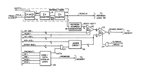
Figure 2 is a block diagram of a portion of the refresh
and overlay logic of the memory refresh/overlay circuit.
Figure 3 is a block diagram of the control portion of
the memory refresh/overlay circuit.
Figure 4 is a timing diagram of various signals which
control the operation of the memory refresh/overlay circuit.
Figure 5 is a memory organization map of the system
containing the present invention.
Figure 6 is a schematic diagram of the refresh timer
circuitry shown in Figure 2.
Figure 7 is a schematic diagram of the refresh address
generator 18 shown in Figure 2.
Figure 8 is a schematic diagram of the refresh control
logic 30 of Figure 3.
Figure 9 is a schematic of the address multiplexers 20
and 22 shown in Figure 2.
Figure 10 is a schematic diagram of the RAS and CAS
logic 34 shown in Figure 3.
Figure 11 is a schematic diagram of the adder circuit
26 shown in Figure 2.
Figure 12 is a schematic diagram of the code/data
overlay logic 28 shown in Figure 2.
DESCRIPTION OF THE PREFERRED EMBODIMENT
Referring to Figure 1, a block diagram o the control
portion of a PCM subscriber multiplexer is shown. Simplistically
speaking, the control portion of the multiplexer contains a
microprocessor circuit 1 which is connected via data bus to memory
2. Typically, the microprocessor address and control bus would be
connected directly to the memory. However, in the present
~2 ~31~L~
invention these buses are intercepted by the memory
refresh/overlay circuit 3. That is, the address and control buses
are routed from microprocessor 1 to memory refresh/overlay circuit
3 where they are manipulated to perform dynamic RAM memory
refreshing and a memory overlay or enlargement scheme. These
buses are then transmitted from memory refresh/overlay circuit 3
to the memory 2 to perform the desired memory accessing function.
The PCM subscriber multiplexer is a remotely located
switching mechanism which connects up to 96 subscriber lines on to
a particular T1 span for switching operations by a central
switching office. The control portion of the multiplexer performs
the required software functions for the multiplexer system. The
heart of the microprocessor circuit 1 is an Intel 8085
microprocessor. Intel is a registered trademark of the Intel
Corporation. An Intel 8086 microprocessor is also adaptable for
use in the present invention. The microprocessor circuit 1
together with the memory 2 provides the decision making logic for
the multiplexer system. All processing, routing, supervision and
administrative functions are performed by the microprocessor
circuit 1 in conjunction with a host processor located at the
central office. The microprocessor circuit 1 and the host
processor communicate via a dedicated channel of a T1 span. The
program code for operating the multiplexer is stored at the
central office and is transmitted to the multiplexer system via
the T1 data link during a power up start phase. This program is
then stored ln dynamic RAM memory located within the multiplexer.
The only permanently resident program in the multiplexer is
located in PROM memory and is the boot strap for loading and
reinitializing the multiplexer software after a power up.
Referring to Figure 2, the REFRESH TIMER comprises
three stages. The first stage is a programmable synchronous
cou~ter 10 which divides the input processor clock signal PCLK by
four or by three. Counter 10 renders this circuit flexible for
use with an Intel 8085 microprocessor which requires a 3 MHz clock
signal or an Intel 8086 microprocessor which requires a 4 MHz
.
~73iL~:~
clock signal. The progran~able counter 10 provides a strapping
option via the CNTCTL lead for determination of whether the
counter 10 divides by three or four.
If the CNTCTL lead ls strapped to a logic low, counter
10 operates as a divide by three counter. If the CNTCTL lead is
strapped to a logic high, counter 10 operates as a divide by four
counter. Counter 10 is connected to dlvide by five counter 12 via
the 1 MHæ lead. The frequency of the signal output by counter 10
is now 1 MHz.
The second stage of the REFRESH TIMER is a synchronous
divide by five counter 12. Divide by five counter 12 takes the 1
MHz signal input and produces a 200 K~z signal as an output on the
200 K~z lead.
The 200 KHz lead connects divide by five counter 12 to
divide by three counter 14. The last stage of the REFRESH TIMER,
counter 14, produces a 15 microsecond clock on the 15 USCLK lead.
This 15 microsecond clock is input to the refresh address
generator 18.
In order for data to be retained by the dynamic memory,
each memory cell must be refreshed at least once every 2
milliseconds. The memory is organiæed such that there are 128
rows of storage cells. Refreshing one row of the 128 rows of
storage cells will refresh all cells associated with that row. If
each of the 128 rows of memory is refreshed sequentially every 15
microseconds, all rows will be refreshed within the required 2
millisecond refresh time period.
The refresh address generator 18 produces the address
of the row to be refreshed during each memory refresh cycle (15
microsecond). To address 128 rows of memory, 7 bits are required.
Address bits are REF0 through REF6 are required to access the 128
rows of the dynamic RAM memory. The 8th bit, REF7, although
transmitted to the memory, is functionally irrelevant to
determining which of the 128 rows of memory cells to be refreshed.
Refresh address generator 20 is an 8-bit binary down
counter. The use of all 8 address bits by counter 20 permits
'7;~
further expansion of this gate array to the full 256K dynamic RAM
memory. The clock signal on the 15 USCLK lead is input to the
refresh address generator 20. Address generator 20 is clocked, so
that it is decremented once each 15 microseconds. Generator 20
provides an address for each of the 128 rows to be refreshed in
response to the clock pulse input on the 15 USCLK lead. On each
successive count of the 15 microsecond clock, generator 20 will
decrement the address of the row to refresh by one and output that
address on the address bus REFO through REF7. In response to
being addressed each row of memory the memory cells of that row
are refreshed.
As shown in Figures 2 and 3, the refresh control logic
30 sends an active low hold request signal via the HOLD lead to
the processor every fifteen (15) microseconds. Refresh control
logic 30 is connected to counter 14 via the 15 USCLK lead. The
microprocessor circuit (processor) is also connected to an input
of the refresh control logic 30 via the hold acknowledge (HLDA)
lead. The refresh control logic is connected to the clock via the
PCLK lead.
In response to the 15 microsecond clock, the refresh
control logic 30 generates the HOLD signal which is transmitted to
the processor. The HOLD signal has the effect of inhibiting
processor's access to memory. This allows the refre~h circuit to
refresh one row of the dynamic RAM memory. Since, the hold
request is generated asynchronously to the processor's operation,
the refresh circuit must wait until the end of a processor
instruction cycle before the processor relinquishes its control to
the refresh circuit. When the processor is ready to relinquish
control, it responds with a signal on the hold acknowledge (HLDA)
lead. For proper operation of the refresh circuit an assumption
is made that the real time of the processor is such that the
processor will acknowledge the hold request well within the 15
microsecond period before the next hold request is transmitted to
the processor by refresh control logic 30.
~2 ~3;~L;~ ~
For example, assuming that the processor has just begun
processing its longest instruction, an 8085 microprocessor running
at a clock rate of 3 MHz will in the worst case acknowledge hold
after seventeen clock cycles or approximately six microseconds.
The dynamic RAM memories typically require between 150 nanoseconds
to Z00 nanoseconds minimum pulse width for the refresh operation.
This circuit minimizes the required time by generating a refresh
pulse for particular row merely one clock cycle after the hold
acknowledge signal is given by the processor. As a result the
processor is held for no greater than 2 clock cycles for the
refreshing operation which results in only a 2 to 5 percent
degradation of processor through put due to the RAM refresh
operation.
The outputs of refresh address generator 18 (REF0
through REF7) are transmitted to multiplexer 20 via a
corresponding bus. In addition, the low byte leads of the
processor address bus (A0 through A7) are connected as another
input to 2-to-1 multiplexer 20. The processor is connected to
multiplexer 20 via the hold acknowledge (HLDA) lead. A value of
logic 0 of the hold acknowledge signal indicates that the low byte
of the processor's address is to be gated through multiplexer 20.
A value of logic 1 of the hold acknowledge signal lndicates that
the refresh address bus (REF0 through REF7~ is to be gated through
multiplexer 20.
In order to refresh a memory location, the next falling
edge of the PCLK signal after the hold acknowledge (HLDA) signal
has been received by refresh control logic 30, logic 30 will
generate a logic 0 on the RRAS lead which is connected to AND gate
36. The R~AS signal when combined with MRAS signal will generate
the DMRAS signal which strobes the refresh address into the
memory.
The 8-bit output of multiplexer 20 is connected to
multiplexer 22 via the low byte 8-bit bus. The other input to
multiplexer 22 is the processor high-byte 8-bit bus address. The
output of multiplexer 22 is connected to the memory via the 8-bit
~.~7~
bus DRAM0 through DRAM7. Control of multiplexer 22 is established
by AND gate ~4 which produces a logic 0 value for gating out the
low byte to memory and the value of logic l to gate the high byte
of the addressed memory. AND gate 24 is controlled by ehe MRAS
signal generated by the RAS and CAS logic 34 and by an externally
delayed version of the MRAS signal, called the DLYMRAS signal.
For normal address transmission from the processor to
memory, the low byte is first transmitted from the processor on
address leads A0 through A7 through multiplexer 20 via the low
byte bus through multiplexer 22 via the DRAM bus to the memory.
When the high byte of the processor address is output on address
leads A8 through A15, it is transmitted through multiplexer 22 via
the high byte bus in response to the operation of AND gate 24 for
a logic l. The high byte is then transmitted via the DRAM bus to
the dynamic RAM memory.
In order for the processor to access a memory location,
the processor outputs the address on the address bus and indicates
the presence of the valid address on the bus via the address latch
enable (ALE signal). See Figure 4. The address on the address
bus is valid and stable on the falling edge of the ALE signal.
This falling edge of the ALE signal is used by the RAS and CAS
logic to generate the MRAS signal. The MRAS signal ANDED with
gate 36 generates -DMRAS signal which is used to strobe the low
byte of address information through multiplexer 22 to the dynamic
RAM memory.
The 30 nanosecond delay line 38 is connected to RAS and
CAS logic 34 via the MRAS lead. In response to the MRAS signal,
the DLYMRAS signal is generated which is a delayed version of the
MRAS signal by 30 nanoseconds. When DLYMRAS signal goes high,
multiplexer 22 which is connected to gate 24 selects the high byte
of the processors address and transmits the address to the dynamic
RAM memory.
The processor's memory access consists of either a READ
or a WRITE operation from the dynamic RAM memory. See Figure 4.
In either event, one of the signals from the processor will go
~L~73~
active low (PRD for a processor read operation and PWR for a
processor write operation). The falling edge of either one of
these signals (-PRD or -PWR) is used to generate an active low
signal DMCAS which strobes the high byte of the processor's
address into the dynamic RAM memory. During the write cycle, the
data from the processor is written into the addressed location on
the rising edge of the -PWR signal. If the PWR signal is
inactive, the dynamic RAM defaults to a read cycle operation. For
a read operation by the processor, data from the dynamic RAM
memory is latched into the processor on the rising edge of the
-PRD signal. The rising edge of either the -PWR signal or -PRD
signal will complete the process of memory access and reset all
flip-flops internal to the CAS and RAS logic 34. The WPRT control
signal from the processor when activated disables the write
operation to the program memory.
Referring again to Figure 2, adder circuit 26 is
connected between AND gate 27 and multiplexer 22. AND gate 27 is
4 bits wide and is connected to sources of logic 0 and logic 1 so
as to construct a 0100 binary pattern, which is equivalent to a
numeric four. AND gate 27 is also connected to code/data overlay
logic 28 via the DATA lead. When A~D gate 27 is enabled by the
signal on the DATA lead, AND gate 27 inputs a four-bit wide binary
equivalent of the number 4 to adder circuit 26.
- Figure 4 shows that during a write access operation,
the low active DMWE signal used to write the data into the dynamic
RAM memory and during the read access operation, the active low
~IBENB signal is used to enable the tristate data bus for receipt
of data by the processor. The PROMENB enables access to a PROM
memory for determining whether the processor current instruction
is a multi-byte instruction or a single byte instruction. This
signal generates the PROMOUT signal input to code/data overlay
logic 28.
Figure 5 depicts the system memory organization. The
software boot strap is located in a PROM memory (not shown)
processor addresses from OH to OFFFH. This represents 4K bytes of
3L~7~
memory. Memory locations 1000H through CFFFH contain the system
software program code. The system software code represents 48K
bytes of memory. Memory locations DOOOH through EFFFH contain the
memory mapped 1/0 locations. The memory mapped I/O locations
comprise 8K bytes.
Data base in the form of office dependent data is
contained in the remaining 4K bytes of static RAM memory beginning
with the memory location FOOOH and continuing to FFFFH.
Within the system software code area (48K bytes from
locations 1000H to CFFFH), a particular area is used as scratch
pad memory and effectively overlaid on top of the program code
area. This area is 16K bytes in length and spans from locations
9000H to CFFFH. The overlay is such that the processor address
output is the same for the program code or the scratch pad area.
The memory are physically separate, but address using the same
address. The total memory area comprises 80K bytes of memory.
Out of that 64K bytes is dynamic RAM memory comprising of 48K
bytes of code and 16K bytes of scratch pad.
Typically, program operation codes are fetched from the
system software code area and no writing is performed within this
area. For efficiency and minimally sized memory considerations,
it is advantageous to overlay a portion of the system software
code area with writeable scratch pad memory. The processor
addresses a particular area for scratch pad memory. In response
- 25 the overlay logic 28 relocates the processor's address to a
different area of dynamic RAM memory for the particular data
access. In this way both code and data can be accessed by the
processor via the same processor address. This scheme effectively
doubles the possible size of the memory associated with the
processor. One bank of memory may contain program code and the
other bank may contain data~
During an OPCODE fetch operation to the memory, the
processor status bits SO and Sl are both at logic 1. Reference
table l below.
~3~
TABLE 1
PROCESSOR STATUS BITS
S0 S1 IO/M REMARKS
1 1 0 OPCODE FETCH
0 1 0 MEMORY READ
1 0 0 MEMORY WRITE
I/O-M=1 disables the access to the memory.
The status bits S0 and S1 are decoded by overlay logic 28 of
Figure 2 as an OPCODE fetch operation. A logic 0 is produced on
the DATA lead which is transmitted to AND gate 27. A logic 0 on
the DATA lead inhibits AND gate 27 from operating and thereby
adder circuit 26 does not add the value of 4 to the upper half of
the high address byte (A12-A15). As a result, the OPCODE fetch
operation occurs normally from the proper address within the
dynamic RAM memory.
During the OPCODE fetch operation, a logic 1 on the
PROMEMB lead is generated on the following edge of the PRD signal.
Reference Figure 4. The PROMENB signal is ~xternally used to
latch the OPCODE read from memory. The latched OPCODE is then
used as an address to the PROM which will decode this OPCODE and
produce the PROMOUT signal which will determine whether the OPCODE
fetched from memory is a single byte instruction or a multi-byte
instruction. This signal is an input to the Data/Code overlay
logic. This determination is important for all ranges in which
code and data are overlaid (that is, they have the same addresses
possible). In the Intel 8085 application, for a single byte
OPCODE fetch, the next memory read is from the data bank of the
memory. A write operation is always to the data bank of the
memory, except during a program loading operation. For multi-byte
instructions, the OPCODE fetch operation is followed by two reads
from the program code area or one read from the code area followed
by a write to the data area of memory.
For accesses (either memory read or memory write) to
the data area, the DATA signal is at logic 1 and AND gate 27 is
enabled to add the particular offset value on the 4 bit strapping
~.~'73:~2~
bus. In the general case, any offset value is possible depending
upon the extent of the implemented scratch pad memory area. In
this case, it is the value 4 in the upper half of the high byte of
the address.
In Figure 2 adder circuit 26 adds the value 4 in the
high order nibble of the upper byte of address to value of the
address transmitted by the processor. As a result~ the processor
accesses a particular area which for an OPCODE fetch would contain
program code; however, the address is offset by adder circuit 26.
The data is then read from a different location of the dynamic RAM
memory based upon the value of the status bits of the processor
and PROMOUT. It is assumed for the above code and data overlay
scheme that the derived processor control signals PC2 and PC3 are
both at logic 1. These signals are generated by other logic
intermediate to the processor and the overlay logic (not shown).
For the possible values of the processor control signals reference
Table 2.
TABLE 2
PROCESSOR CONTROL SIGNALS
Code Access
or
PC2 PC3 Data Access
0 0 Data For data initialization; Address Offset
0 1 Code For loading code; No Offset
1 0 Data For loading data; Address Offset
1 1 * Program execution; Offset only during
data access under program control.
The DMWE and DIBENB signals are inhibited for the
memory access in the range of locations 0000H through OFFFH and
DOOOH through FFFH. Reference the memory map in Table 3.
12
.
.
~L~7~
TABLE 3
MEMORY MAP
Addre 5 S Remarks
OOOOH -DMWE and -DIBENB signals are inhibited
o
o
OFFFH
101000H Code area. -DIBNB signal always enabled.
o -D~E slgnal enabled except for WPRT=1.
oo
8FFFH
9000H Code and Data overlay area.
o -DIBENB signal always enabled.
o -DMWE signal can be inhibited if WPRT=l
o However, -DMWE signal will be enabled even
20CFFFH if WPRT=1, if the access is to data.
DOOOH -DMWE and -DIBENB signals are inhibited.
o
o
FFFFH
Again, for access to data memory the address in the
range 9000H through CFFFH is offset by 4000H by adder 26 before
the address is transmitted to the dynamic RAM memory. Note that
for code access to the same locations the address is not offset by
adder 26. The high going edge of either PWR or PRD signals will
end the processor access to memory. Reference Figure 4.
Figure 6 depicts the logic implementations of the
refresh timer shown in Figure 1. The PCLR lead is connected to
the clock input of D-type flip-flop 101. The strapping option
CNTCTL lead is connected between logic O or logic 1 and NAND gate
103. NAND gate 103 is connected to NAND gate 102. The reset
signal CLEARB is connected to the clear input of each D-type
flip-flop 101, 104, 105, 107, 109, 110 and 112.
The PCLK signal is either a 3 MHz or 4 MHz signal from
the processor clock. For a 3 MHz PCLK signal, the CNTCTL lead is
strapped to a logic O and for a 4 MHz PCLK signal, the CNTCTL lead
~7~
is strapped to a logic 1. NA~D gate 102 is connected to the D
input of flip-flop 104. As a result, for either a 4 or 3 MHz PCLK
signal input, flip-flop 104 produces a 1 MHz signal on the Q
output. Flip-flops 101 and 104 produce the divide by 3 or 4
function.
The Q output of flip-flop 104 is connected to the clock
input of flip-flops 105, 107 and 109. The n output of flip-flop
105 is connected to NOR gate 106. The output of NOR gate 106 is
connected to the D input of flip-flop 107. The clock input of
flip-flop 107 is connected to the Q output oE flip-flop 104. The
Q output of flip-flop 107 is connected to the D input of flip-flop
105. The -Q output of flip flop 107 is connected to one input of
NAND gate 108. The other input to NAND gate 108 is connected to
the Q output of flip-flop 105. The output of NAND gate 108 is
connected to the D input of flip-flop 109. The clock input of
flip-flop 109 is connected to the Q output of flip-flop 104. The
Q output of flip-flop 109 is connected to the clock input of
flip-flop 110 and provides the 200 KHz output signal. Flip-flops
105, 107 and 109 along with gates 106 and 108 provide a divide by
5 function.
The -Q output of flip-flop 109 is connected to one
input of NOR gate 106. As a result of the input PCLK signal 3 or
4 MHz, the Q output of flip-flop 109 is now a 200 KHz signal.
The 200 KHz signal is also transmitted via a connection
from the Q output of flip-flop 109 to the clock input of
flip-flops 110 and 112. The Q output of flip-flop 110 is
connected to one input of NAND gate 111. The output of NAND gate
111 is connected to the D input of flip-flop 112. The Q output of
flip-flop 112 on the 15 USCLK lead is a 15 microsecond signal
which is used to generate hold request to the processor for
refreshing dynamic RAM memory and generating refresh address. The
- Q output of flip-flop 112 is also connected to the second input of
NAND gate 111 and the D input of flip-flop 110. Flip~flops 110
and 112 and gate 111 providP the 15 microsecond clock signal.
..
~7~
Figure 7 depicts the details of the refresh address
generator 18 shown in Figure 2. Flip-flops 120 through 127 form a
synchronous 8-bit binary down-counter. Each flip-flop 120-127 has
its CLK input connected to the 15 microsecond clock signal via the
15 USCIK lead. The clear signal is connected via the CLRB lead to
the preset input of each flip-flop 120-127. The -Q output of each
flip-flop 120-127 produce one refresh address lead output
REFO-REF7 respectively~ For refreshing 64K of dynamic RAM memory
7 bits of address information are required. However, 8 bits of
addressing information are produced via the REFO through REF7
leads. The most significant address bit (REF7) is insignificant
for the particular operation of the disclosed circuit and is
therefore a don't care function. Since the implemented design is
a modulo 255 counter the low order 7 bits are effectively a modulo
127 counter required to refresh 64K of a dynamic RAM. The 8-bit
REF7 maybe used for extended memory applications up to 256K of
dynamic RAM.
Each flip-flop of the refresh generator 18 is clocked
on the rising edge of the 15 USCLK lead. As a result, each
refresh lead REFO through REF7 outputs the address required to
refresh the dynamic RAN memory. Each successive appearance of the
15 USCLK lead decrements the address output on leads REFO through
REF7 by 1. Therefore, a new address is output to multiplexer 20
at each 15 microsecond time period. As dynamic RAM memory is
accessed via an address, it is automatically refreshed. The CLRB
signal can be used to clear flip-flops 120 through 127 on
power-up.
Figure 8 shows the details of the refresh control logic
30 of Figure 2. The 15 USCLK lead is connected to flip-flop 130.
The -Q output of flip-flop 130 produces the active low hold
request signal on the HOLD lead which is transmitted to the
processor. The processor inverted clock signal is transmitted to
the clock input of flip-flop 133 via the -PCLK lead.
When the processor responds to the hold request via the
hold acknowledge signal on the HLDA lead, it is transmitted
through NAND gate 131, through NOR gate 132 and latched in
flip-flop 133 on the next falling edge of PCLK signal. The -Q
output of flip-flop 133 is the active low -RRAS signal which is
transmitted to RAS a~d CAS logic 34. The -RRAS signal gated
through RAS and CAS logic 34 generates the RAS signal for one
period of PCL~ which will strobe the refresh address into the
dynamic RAM.
Flip-flop 133 has its -Q output connected to the clock
input of flip-flop 134. The -Q output of flip-flop 134 is
connected through NOR gate 135 to the clear input of flip-flop 130
at the end of refreshing cycle to remove hold request to the
processor. Either the CLR signal or the -Q output of flip-flop
134 will be gated through NOR gate 135 and reset flip-flop 130 for
the occurrence of the next 15 microsecond clock period.
Figure 9 depicts the details of multiplexers 20 and 22
of Figure 2. Multiplexer 20 is comprised of NOR gate combinations
140 through 147. Combination gates 142 through 146 are not shown.
Processor address bit O (SLA0) is input to combination gate 140
along with refresh address bit 0 (REF0). The status of the hold
acknowledge signal HLDA determines which of the address bits is
gated through multiplexer 20.
If the HIDA lead is active (logic 1) refresh bit 0,
REF0 signal, is gated through combination gate 140 to the input of
NAND gate 150. Combination gates 141 through 147 operate
similarly with address bits SLAl through SLA7 and refresh bits
REFl through REF7, respectively. For an inactive hold acknowledge
signal HLDA equal logic 0, the processor address bit SLA0 is
transmitted through combination gate 140 to NAND gate 150. And
similarly, for processor address bits SLAl through SLA7 and
combination gates 141 through 147, respectively.
The DLYMRAS signal and the MRAS signal control the
second stage multiplexing, multiplexer 22. Multiplexer 22 is
comprised of NAND gates 150 through 165 and 170 through 177. Thc
output of combination gates 140 through 147 is connected to NAND
gates 150-164 (even numbered ones only). Each of the odd numbered
16
-
. .
~7~
NAND gates 151 through 165 is connected to one of the bits of the
high byte of the processor address tHIGH-ADDO through HIGH-ADD7).
NAND gates 150 and 151 are connected to the inputs of
NAND gate 170. For a processor access of the memory, the HLDA is
inactive (low). As a result, the processor low-byte address bits
SLAO through SLA7 are gated through the NAND gates 170-177 on the
DRAMO through DRAM7 leads and transmitted to the dynamic RAM
memory. After the low-byte is strobed into the DLYMRAS signal
goes active and gates processor high-byte address on the DRAMO
through DRAM7 leads to the dynamic RAM.
For a active HLDA signal, the refresh address bits REFO
through REF7 are gated through NAND gate 170-177 on the output
leads DRAMO through DRAM7. For an active DLYMRAS and an active
MRAS signa] the high address bits (HIGH-ADDO through HIGH-ADD7)
are gated through on to the DRAMO through DRAM7 leads.
Figure 10 is a detailed schematic of the RAS and CAS
logic 34 of Figure 2. Some of the input signals to this logic are
developed by the microprocessor circuit. The MMIOA signal is
normally low except for processor addresses in the range of DOOOH
through EFFFH which is reserved for the memory mapped I/O
locations. If the MMIOA signal is high, then the read and write
control signals (PRD and PWR) from the processor are disabled.
Similarly, the FOACC signal is normally low, except for processor
addresses in the range from OOOOH through OFFFH and FOOOH through
FFFFH, which are reserved for dedicated processor ROM and RAM
applications.
For typical accesses of a memory location, the HLDA and
I/O-M signals will be at logic 0. The address will be put on the
address bus and the falling edge of the ALE signal indicates that
the address is valid. The ALE signal clocks flip-flop 181 and the
-Q output of flip-flop 181 is the MRAS signal. The Q output of
flip-flop 181 is connected to the D-input of flip-flop 182 and is
the intermediate control output BMRAS. The -Q output of flip-flop
182 is the column address select signal CAS.
The -Q output of flip-flop 181 is connected to NAND
gate 184 along with the RRAS lead from the refresh control logic
30 of Figure 3. They are combined by NAND gate 184 to produce the
row address select signal RAS. The processor read signal PRD is
connected through NOR gate 180 to the clock input of flip-flop 182
and an inverted form i5 transmitted to the clock input of
flip-flop 183.
The processor write signal PWR is connected to inputs
of OR gate 1~0 and to NAND gate 185. The I/O-M lead is connected
to an input of NAND gate 185 and to NAND gate 187. The WPRT
signal is connected to an input of NOR gate 189 along with the
derived DATA signal from the code/overlay logic 28~ Gate 189 is
connected to an input of gate 186 along with the FOACC signal and
the MMIOA signal. The FOACC and MMIOA signals are produced as a
decode of the microprocessor address. The output of gate 186
produces the write enable signal transmitted to memory.
The-clear signal CLRB is input to NAND gate 187 along
with the I/O-M signal and the Q output of flip-flop 183. The
output of gate 187 is used to clear flip-flops 181 and 182 through
NOR gate 188. The HLDA signal is connected to the other input of
NOR gate 188. The PRD, MMIOA, FOACC and I/O-M signals are a
logically combined by OR gate 190 to produce the DIBENB signal for
strobing memory.
Shown in Figure 11, is a detailed schematic of the
adder circuit 26 of Figure 2. Although, for the present invention
only two address-bits requires modification for code and data
overlaying, this scheme is readily adaptable to completely overlay
all locations of code and data memory.
During a data access, from the area in which program
code typically resides, the CODE signal is at logic 0. The CODE
signal along with address bit SLA14 from the processor are
connected to exclusive OR gate 192. When a data access, is
requested, address bit SLA14 is incremented by 1 and as result the
output of exclusive OR gate 192 is a new high address bit 6
(HIGH-ADD6). In addition, the new high address bit 6 is combined
18
~' -
,
~7~
with the old address bit SLA 14 by ANI) gate 193 to carry any
overflow from this addition operation. The overflow from this
addition is carried into address bit 15 SLA15 via a connection
from the output of gate 193 to an input to exclusive -OR gate 194,
where it is also exclusive -OR'ed witll the existing value of
address bit 15 to produce the high order bit of the high byte of
address (HIGH-ADD7). This operation has effectively added 4000H
to the address that was present on address leads SLA0 through
SLA15.
Figure 12 is a schematic showing the details of
implementation of the code/data overlay logic 28 of Figure 2. The
overlay active signal (OVRLACC) is normally at logic 1 and is
generated as a decode of the microprocessor address. If this
signal is at logic 0, the current processor access is indicated to
be within the range of the overlaid memory and data, in this case
9000H through CFFFH. If the overlay active signal OVRLACC is at
logic 1, then the CODE signal is at logic 1 and adder circuit 26
will not add any offset to the processor address. The processor
address may be offset by the adder circuit 26, if the overlay
active signal is at logic 0, depending on control inputs PC2 and
PC3. Reference Table 2.
The S0 signal is transmitted through NOR gate 201 to
the D-input of flip-flop 202. The S0 bit (see table 1) is latched
by flip-flop 202 and the output of flip-flop 202 is transmitted to
the D-input of flip-flop 203. The S1 status bit of the processor
is transmitted through NAND gate 207 to AND gates 206, 210 and
216. During program execution, the first processor cycle is an
OPCODE fetch from program memory. The status bits S0 and S1 (see
table 1) are decoded as a OPCODE fetch which clocks flip-flops
202, 203 and 204. The D-input to flip-flop 204 is the status bit
S1 transmitted through gate 207 and 211. As a result, the Q
output of flip-flop 204 is transmitted through gate 212 and gate
214 to produce a logic 1 on the CODE lead. Correspondingly a
logic 0 is simultaneously produced on the DATA lead through
inverter 215.
19
~7~ 4
During an OPCODE fetch cycle the PROMENB signal takes
on a logic 1 value. The PROMENB signal is used as a clock input
to an external latch (not shown) in which the OPCODE is used as an
address to PROM memory (not shown). The memory will decode the
fetched instruction to determine whether the OPCODE is a single
byte or multi-byte instruction. For a single byte instruction the
value of the PROMOUT signal will be logic 1 and for a multi-byte
instruction logic 0.
For Intel 8085 application, a single byte OPCODE fetch
is followed by any memory accesses to the data area. If the
PROMOUT signal is high, any further memory accesses will force the
CODE signal to go low and the DATA signal to go high. On the
other hand, for multl-byte OPCODE fetch, the PROMOUT signal will
be low and two following memory read cycles will be from the code
area. Accordlngly, the CODE signal will be high for two memory
reads following OPCODE fetch. Any further read cycles will be
made from the data area. Note that any write cycle to the memory
is to the data area only.
Although the preferred embodiment of the invention has
been illustrated, and that formed described in detailed, it will
be readily apparent to those skilled in the art that various
modifications may be made therein without departing from the
spirit of the invention or from the scope of the appended claims.
- :.
'
-