Note: Descriptions are shown in the official language in which they were submitted.
1~35~8
TITLE OF THE INV~NTION
OPTICAL MULTICONDUCTOR OF SILICA GLASS TYPE
BACKGROUND OF THE INVENTION
1. Field of the Invention
The present invention relates to optical multi-
conductors of the silica glass type which ar~ suited
as image transmitters for various image scopes for
industrial, medical and other uses, especially as image
transmitters for medical image scopes.
2. Description of the Prior Art
Image scopes transmitting sharp images and
having the smallest possible diameter are required for
directly observing in detail portions or sites which
are usually difficult to observe, such as the interior
of hot blast furnaces, the interior of atomic reactors
exposed to radiation, internal portions of the human
body or animals, narrow or constricted inner portions of
devices, etc.
Conventional image scopes have an optical
multiconductor serving as an image transmitter and
comprising a multiplicity of optical fibers of the multi-
component glass type. As is well Icnown, however, multi-
component glass is low in resistance to heat and radia-
tion and generally contains large quant'ities of
. ~
.
1~'73~
impurities, which have heretofore presented extreme
difficulties in fabricating thinner optical fibers,
consequently imposing limitations on the reduction of
the diameter of the optical multiconductor.
In contrast, silica glass has high resistance
to heat and radiation, is excellent in drawability and
therefore has the advantage that a bundle of a large
required number of optical fiber preforms, each composed
basically of a core and a cladding layer, can be easily
10 - drawn into a multiconductor of reduced diameter which
can in no way be produced from multicomponent glass.
In the case of optical fiber preforms in which
the core is made of doped silica glass, different
dopants are usable in varying amounts to increase the
refractive index difference between the core and the
cladding layer, with the result that leakage of light
can be prevented effectively even with a thin cladding
layer. Accordingly, the drawing ratio can be increased
to afford an optical multiconductor of decreased
diameter.
For preparing such optical fiber preforms
having a core of doped silica glass, there is a need to
use, for example, core rods of doped silica glass,
whereas such core rods heretofore used are not those
prepared for producing image scopes but are only those
.. 'I
1~7351~
intended for the fabrication of communication optical
fibers. Moreover, the conventional core rods have a par-
aboric refractive index distrib~tion ~hat is the refractive
index greatly decreases from the center of the rod toward
S its surface as indicated by Curve 1 in Fig. 7.
Accordingly, when these core rods are used for producing
an optical multiconductor, the multiconductor obtained
has the problem that each fiber serving as a picture
element is bright only at its central portion and
greatly increases in darkness from the center toward the
outer periphery. Thus, as the diameter of the multi-
conductor decreases, the image transmitted therethrough
becomes less easy to view.
SUMMARY OF THE INVENTION
The main object of the present invention is
to provide an optical multiconductor which has fiber
cores of the graded index type and which nevertheless is
free of the above problem and is therefore capable of
transmitting sharp and bright images although having a
reduced diameter.
Stated more specifically, the present inven-
tion provides an optical multiconductor of the silica
glass type characterized in that the multiconductor
comprises 102 to 107 optical fibers of the slica glass
type fused to one another, each of the optical fibers
~27351~3
comprising a core made of doped silica glass and having
an average radius of rl, and a cladding layer made of a kind of
silica glass and formed on the core, the core having a
~, refractive index distribution satisfying the fo~lowing
expression tl):
n2 ~ nl + 0.50(nO - nl) (1)
wherein nO is the refractive inde~ of the core at its
center, nl is the refractive index of the core at its
outermost portion, and n2 is the refractive index of
the core at a position centered about the axis of the
core and having an average radius of 0.65rl.
BRIEF DESCRIPTION OF T~E DP~AWINGS
Fig. 1 is a sectional view of an optical
multiconductor embodying the present invention;
Fig. 2 is an enlarged fragmentary view in
section showing the embodiment of Fig. l;
Fig. 3 is a sectional view of another optical
multiconductor embodying the present invention;
Fig. 4 i5 an enlarged fragmentary view in
section showing the embodiment of Fig. 3;
Fig. 5 is a sectional view of another optical
multiconductor embodying the present invention;
Fig. 6 is an enlarged fragmentary view in
section showing the embodiment of Fig. 5;
Fig. 7 is a diagram showing the refractive
? 4-
'I
1.;~73S~
index distributions of the cores of optical fibers
constituting optical multiconductors; and
Fig. 8 is a sectional view showing an example
of image scope incorporating the optical multiconductor
of the invention as an image transmitter.
~ ETAILE~ DESCRITION OF THE INVENTION
Fig. 8 shows an optical multiconductor 1 of the
present invention serving as an image transmitter, an
objective lens 2 mounted on the front end of the multi-
conductor 1, a removable eyepiece 3 mounted on the rearend of the multiconductor 1, an ocular lens 31 installed
within the eyepiece 3 and an illuminating light guide 4.
At least a specified length of front end portion of the
light guide 4 is housed in a protective tube 5 coex-
lS tensive with the multiconductor 1 for protecting theconductor 1 over the entire length thereof. The remain-
ing rear portion of the guide 4 is branched and encased
in a protective tube 6. Whén heat resistance, rather
than flexibility, is required of the image scope, the
protective tubes 5 and 6 are made of a metal such as
stainless steel, titainum or copper. When flexibility
is especially required for medical use-,et~, these tubes are
made of a flexible organic high polymer such as nylon,
polyethylene, polypropylene or polyvinyl chloride.
When the present device is to be used as a medical
, -5-
~;~735~8
image scope, the protective tube 5 houses therein, in
combination with the multiconductor and in addition to
the light guide 4, other means such as water conduit,
gas conduit, forceps, baloon, tip articulation ,laser
fiber, electric coagulator or the like.
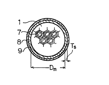
Figs. 1 to 6 show optical multiconductors 1
and a multiplicity of optical fibers 7 constituting each
multiconductor 1. According to the embodiment shown
in Figs. 1 and 2, each of the optical fibers 7 comprises
a core 71 and a cladding layer 72 formed on the core 71.
The adjacent cladding layers 72 are fused and joined
to one another. According to the embodiment of Figs.
3 and 4, a first cladding layer 72 over a core 71
further has thereon a second cladding layer 73, and the
adjacent cladding layers 73 are joined to one another
by fusion. Further according to the embodiment of
Figs. 5 and 6, the second cladding layer 73 is covered
with a third cladding layer 74, and the adjacent third
cladding layers 74 are joined to one anther by fusion.
I~dicated at 8 is a skin layer provided over the outer-
most portion of the multiconductor 1, and at 9 a
reinforcing layer covering the skin layer 8 and made,
for example, of organic high polymer cured by UV rays or
heat or thermoplastic organic high polymer.
With reference to Figs. 1 - '6 indicated
.
1~73518
at: Df is the diameter of the optical fiber 7, at Dc
t.he diameter of the core 71 (which has an average radius
of rl), at Tl the thickness of the first cladding layer
72, at T2 the thickness of the second cladding layer 73,
and at T3 the t.hickness of the third cladding layer 74.
It is further assumed that the multiconductor 1 has a
diameter Dm, the skin layer 8 has a thickness Ts and the
reinforcing layer 9 has a thickness Tp.
Usually the optical multiconductor 1 can be
prepared from 102 t.o 107, preferably 103 to 5x1O6~optical
fiber preforms each having a circular cross section and a
structure corresponding to the optical fiber 7 in cross
section, by filling the preforms in an orderly arrange-
ment into a skin pipe (for forming the skin layer 8 of
Fig. 1, 3 or 5) of natural silica glass or synthetic
silica glass, preferably of synthetic silica glass, and
subsequently drawing the assembly. During the drawing,
the optical fibers are fused to one another and thereby
deformed in cross section to a hexagonal shape as seen
in Fig. 2, 4 or 6 or to a shape slightly or considerably
collapsed from the hexangonal shape. Unless otherwise
stated in the following description, the values DE, Dc,
Tl, T2 and T3 typically show the values of corresponding
parallel portlons of hexagonal cross sections as
illustrated, while as to the fibers of a shape considerably
-7
lX73~
deformed from a hexagon, the values given are those of
the corresponding illustrated parallel portions of a
hexagon which is equal in area to the deformed shape.
The refractive index distributlon of the core 71 will be
described with reference to Fig. 7 assuming that the
core has a circular cross section with an average radius
of rl. However, when the core is hexagonal or of a
shape other than circular in cross section, the descrip-
tion is to be interpreted as being given as to a circle
which is equal in area to the section of the core.
The core 71 of each optical fiber 7 occupies pref-
erably at least 2~% of the ~iber in cross sectional area
(hereinafter area ratio ). If the core area ratio is less than
20~Jthe amount of ~ight to be transmitted through the core 71
is small, and it is difficult to transmit a bright image
therethrough. If thë core area ratio is excessively
great, the cladding layer becomes too thin unless the
flexibility of the multiconductor is sacrificed, present-
ing difficulty in transmitting sharp images due to
obscurity. Accordingly, the core area ratio is prefer-
ably up to 60%, more preferably 25 to 50~.
With reference to Fig. 2, the values Df and
Tl are about 3 to about 16 ~m and abaut 0.5 to about
5 ~m, respectively, preferably about 4 to about 15 ~m
and about l to about 4 ~m, respectively. With reference
~;~'73~
to Fig. 4, the values Df, Tl and T2 are about 3 to about
16 ~m, about 0.3 to about 4 ~m and about 0.01 to about
2 ~m, respectively, preferably about 3.5 to about 10 ~m,
about 0.5 to about 2.5 ~m and about 0.01 to about 1.5
~m, respectively. With reference to Fig. 6, the values
Df, Tl, T2 and T3 are about 3 to about 16 ~m, about
0.03 to about 1.2 ~m, about 0.15 to about 2.5 ~m and about
0.01 to about 1.5 ~m, respectively, preferably about 3.5
to about 15 ~m, about 0.05 to about 1.0 ~m, about 0.2
to about 2.0 ~m and about 0.05 to about 0.8 ~m, respec-
tively.
Referring to Fig. 7, Curve 2 is a refractive
index distribution curve of the core 71 of each optical
fiber 7 constituting the multiconductor of the invention.
For reference, Curve 1 is also given which is the
refractive index distribution curve of a core rod for
preparing a usual communication graded index-type optical
fiber. With Curve 2, the difference (~n) between the
refractive index nO of the core 71 at its center rO
(where the core usually has a maximum refractive index)
and the refractive index nl of the core at its outermost
portion rl (where the core usually has a minimum
refractive index), i.e. (nO - nl),is 0.015 to 0.040,
preferably 0.02 to 0.035.
In the refractive index dis'tribution
1~7~8
represented by Curve 2, the refractive index decreases
gently in the section of the core from its center rO to
the portion thereof having an average radius of r2, i.e.
0.65rl, whereas the refractive index decreases greatly
in the core section ranging from r2 to rl in average
radius, i.e. the outer core section up to the outermost
portion of the core. In other words, the variations in
the refractive index are small in the section of from
rO to r2. Moreover, the refractive index n2 at the
position of radius r2 is greater thàn nl ~ O.S(~n~ (e.g.
when ~n is 0.025, nl + 0.5 x 0.025 = nl + 0.0125).
Thus, the core 71, although of the GI type in the
distribution of refractive indexes, is small in the
reduction of refractive index and is not smaller than
lS a value in this index in the section from the center rO
to the radius r2, so that the core has sufficiently
useful brightness in this section and also in a somewhat
outer region thereof.
For the reason stated above, it is desired
that the variations in refractive index be great in the
outward portion of the core 71 and be more gentle in
the central portion of the core. It is therefore desired
that the refractive index n2 at r2 satisfy the following
expression (2).
n2 2 nl + 0.65(nO - nl) ' (2)
--1 0--
~'~735~8
In addition to the refractive index n2 at
r2 (=0.65rl) thus defined, it is also desirable that
Curve 2 have the refractive index n3 at r3 (=0.5rl)
and/or the refractive index n4 at r4 (=0.33rl) which
are given by the following expressions (3) to (6),
respectively.
n3 _ nl + 0.55(nO - nl), (3)
preferably
n3 2 nl + 0.67(nO - nl). (4)
n4 _ nl ;t 0.60(nO - nl), (5)
preferably
n4 2 nl + 0.70(nO - nl). (6)
More desirably, Curve 2 has a refractive
index of nl + 0.5(nO - nl) at the position of an average
radius 0.7rl, in addition to the foregoing refractive
index distribution conditions.
The refractive index distribution of the core
described above can be realized by using a dopant, such
as germanium or phosphorus, which acts to increase the
réfractive index of silica glass a~d controlling the
amount of the dopant by the VAD, CVD or like process
according to the specified refractive index distribu-
tion. Halides of the above dopant 9uch as germanium tetra-
chloride are preferably used as a dopant precursor.
According to the present invention, the core
, --11--
71 of the optical fiber 7 may have only one cladding
layer 72 as in the embodiment of Fig. 2 or two or three
cladding layers which are different from one another
in refractive index as seen in Fig. 4 or 6. Generally
from the viewpont of sharpness of transmitted images,
the difference between the refractive index nl (usually,
minimum refractive index) of the outermost portion of
the core 71 and that of the cladding layer 72 is
preferably greater, while the core 71 may preferably be
provided with at,least two cladding layers.
According to the embodiment shown in- Fig. 2,
the difference between the refractive index nl of the
outermost portion of the core 71 and the refractive
index of the cladding layer 72 may be zero but is
preferably at least 0.006, more preferably at least 0.008,
most preferably at léast 0.010. With the embodiment
shown in Fig. 4, it is desired that the first cladding
layer 72 be preferably at least 0.006, more preferably
at least 0.008, most preferably at least 0.010, lower in
refractive index than the minimum refractive index nl
of the core 71 at its outermost portion and also
preferably at least 0.004, more preferably at least 0.008,
most preferably at least 0.010, lower than the second
cladding layer in refractive index. With the em,bodiment
shown in Fig. 6, it is desirable that the first cladding
, -12-
: ~ . .. . .
.: :
~;~735~8
layer 72 be preferably at least 0.008, more preferably
at least 0.010, most preferably at least 0.012, lower
in refractive index than the minimum refractive index
nl of the core outermost portion and also lower than
any one of the second and third cladding layers in
refractive index, and that the second cladding layer
have a lower refractive index than the third cladding
layer. Stated more specifically, the first cladding
layer 72 is preferably at least 0.002, more preferably
at least 0.004, lower than the second cladding layer 73
in refractive index, while the second cladding-layer 73
is preferably at least 0.004, more preferably at least
0.008, most preferably at least 0.010, lower than the
third cladding layer 74 in refractive index.
The cladding layer 72 of Fig. 2, the first
cladding layer 72 of Fig. 4 and the first cladding layer
72 and the second cladding layer 73 of Fig. 6 are
preferably made of silica glass doped with fluorine
and/or boron or with a dopant composed primarily of at
least one of these elements. More preferably, these
layers are made of pure silica glass doped with BC13,
BF3 or a mixture thereof as a dopant precursor. On
the other hand, the second cladding layer 73 of Fig. 4
and the third cladding layer 74 of Fig. 6 may be made of
silica glass doped with at least one o~ various. dopa~nts, but
? 13-
1~73518
it is desirable to prepare these layers from silica
glass at least 1800 C in drawing temperature, for
example, pure silica glass, especially one having a
purity of at least 99.99 wt. %. The following advantage
will then result. The above-mentioned drawing temper-
ature is defined as the lowest temperature at which
when a tube made of the silica glass to be tested and
measuring 23 mm in inside diameter and 26 mm in outside
diameter is softened by heating and drawn into a tube,
2.3 mm in inside diameter and 2.6 mm in outside diamter,
at a rate of 0.5 m/min, the tube can be drawn under a
tension of not higher than 500 g.
Generally, sharp transmitted images can be
obtained when the optical fibers present in the portion
of the multiconductor 1 within at least 80% of the
radius from the center of its cross section are fused to
one another into a honeycomb structure which is regular
to the greatest possible extent. (The portion within 80%
of the radius may include a locally slightly collapsed
honeycomb structure, darlc points or other defects,
while the honeycomb structure need not: always be a set
of geometric hexagons but can be a set of slightly
deformed hexagons.) Such a multiconductor includes a
relatively small number of optical fibers, e.g. about
25 1,000 to 5,000 fibers, has a small outside diameter Dm
-14-
35~8
of up to 0.8 ~n and is suited to medical uses, especially
as an angioscope. Multiconductors of the above structure
can be obtained generally by using for the outermost
layer (the second cladding layer 73 of Fig. 4, the third
cladding layer 74 of Fig. 6, or the like) of the optical
fiber 7 a glass material (such as the above-mentioned
pure silica glass) having a higher drawing temperature
than the glass for the inner layer(s) (although the core
forming glass can be equal to or slightly higher than
the outermost layer glass material in drawing tempera-
ture), and drawing a bundle of optical fiber preforms
at the drawing temperature ôf the glass material or
at a slight]y higher temperature. The glass material
forming the outermost layer then exhibits a minimum
degree of flowability required for drawing, acting to
prevent an excessive flow (which would give an
irregular cross section to the optical fibers) even if
the glass mataterial for the inner layer exhibits great
flowability.
With reference to Figs. 1, 3 and 5, the skin
layers 8 are preferably at least about 3 ~m, more
preferably S to 20 ~m,in thickness. The reinforcing
layers 9 are preferably at least about 5 ~m, more
preferably 10 to 150 ~m, in thickness.
The optical multiconductors of the present
~73S18
invention are useful as image transmitters for image
scopes for industrial and medical uses, especially for
medical image scopes including angioscopes and endoscopes
for various tubes or ducts in the body such as the
coronary artery, oviduct, urinary tract and bile duct,
gastroscopes, hysteroscopes, cystoscopes, embryoscopes,
otoscopes, rhinoscopes, ophthalmoscopes, encephaloscopes,
arthroscopes, dental image scopes, etc.
For use as the image transmitters of medical
10 image scopes, the optical multiconductors of the inven- -
tion afford sharp images and are therefore very
desirable when filfilling the following requirements
Il) to (4).
(1) Like the embodiment of Fig. 4 or 6, the multi-
conductor has two or three cladding layers.
{2) The second cladding layer 73 of Fig. 4 or the
third cladding layer 74 of Fig. 6 is made of silica
glass at least 1800 C in drawing temperature,
preferably pure silica glass, more preferably pure silica
glass having a high purity of at least 99.99 wt. %.
(3) The core 71 of each optical ~iber 7 of the
multiconductor occupies at least 20% of the fiber in
cross sectional area.
(4) The values Df, Tl and T2 in Fig. 4 ~re prefer-
ably 3.0 to 8.0 ~m, 0.5 to 1.5 ~m and 0.03 to 0.6 ~m,
; -16-
1~735~113
respectively, preferably 3.5 to 6.5 ~m, 0.7 to 1.2 ~m
and 0.05 to 0.4 ~m, respectively, more preferably 4.0
to 5.5 ~m, 0.8 to 1.0 ~m and 0.07 to 0.2 ~m, respectively.
The values Df, Tl, T2 and T3 in Fig. 6 are 3.0 to 8.0 ~m,
0.02 to 0.7 ~m, 0.1 to 1.5 ~m and 0.02 to 0.6 ~m,
respectively, preferably 3.5 to 6.5 ~m, 0.05 to 0.4 ~m,
0.2 to 1.3 ~m and 0.05 to 0.4 ~m, respectively, more
preferably 4.0 to 5.5 ~m, 0.1 to 0.3 ~m, 0.4 to 1.0 ym
and 0.08 to 0.3 ~m, respectively.
Further for use as the image transmitters of
the above-mentioned endoscopes and angioscopes, especially
of angioscopes, the multiconductors of the invention
preferably fulfill the following requirements (5) to (7)
in additior to the foregoing requirements (1) to (4).
(5) The multiconductor comprises 1,000 to 5,000,
preferably 2,000 to 4,000, optical fibers.
(6) The outside diameter (Dm + 2~s) of the skin
layer 8 is about 0.1 to about 0.8 mm, preferably about
0.2 to about 0.6 mm.
(7) The protective tube 5 of the image scope of
Fig. 8 is up to 3 mm, preferably up to 2.5 mm,in
outside diameter and further has an outside diameter
of up to about 1.8 mm over the 5- to 15-cm-long front
end portion of the tube 5.
Further when the multiconductors of the
-17-
- i .
'
--.~ , ' ~
~ .
.
1;~735~3
the invention are to be used as the image transmitters
of endoscopes for the gastrointestinal organs such as
the esophagus, stomach and intestines, it is desired
that the conductors fulfill the following requirements
t8) to (10) in addition to the foregoing requirements
tl) to (4),
(8) The multiconductor comprises 5,000 to 30,000,
preferably 8,000 to 25,000, optical fibers.
(9) The outside diameter (Dm + 2Ts) of the skin
layer 8 is about 0.2 to about 1.5 mm, preferably
about 0.4 to about 1.0 mm.
(10) The protective tube 5 of the image scope of
Fig. 8 is about 3 to about 10 mm, preferably about 4
to about 7 mm, in outside diameter.
Further when the multiconductors of the inven-
tion are to be used as the image transmitters of hystero-
scopes, cystoscopes, embryoscopes, arthroscopes and
endoscopes for other organs, especially as those for
precision observation endoscopes in place of conven-
tional lens scopes, it is desirable that the conductors
fulfill the following requirements (11) to (13) in
addition to the foregoing requirements (1) to (4).
(11) The multiconductor comprises 30,000 to 100,000,
, preferably 50,000 to 100,000, optical fibers.
25 ~12) The outside diameter (Dm + 2Ts ) of the skin
~ .
, -18-
,
.
:'
.
- . ~ ~ . .
- : . ', ~: .
~'73~:;18
layer 8 is about 0.5 to about 3.0 mm, preferably about
1.0 to about 2.5 mm.
(13) The protective tube 5 of the image scope of
Fig. 8 is about 2 to about 10 mm, preferably about 3
to about 7 mm, in outside diameter.
Examples 1-31 and Comparative Examples 1 and 2
Listed in Table 1 are the detailed structure
of optical fiber preforms used in each of the above
Examples and Comparative Examples, the structure of an
optical multiconductor obtained in each example by
compactly filling a specified number of optical fiber
preforms (given in the line of symbol N in the structure
of multiconductor in the table) into a pure silica glass
tube and drawing the assembly at 2100 C, and the
quality of images transmitted throught the multiconduc-
tor. Each refractive index value listed was determined
at 20 C using infrared rays of 0.90 ~m in wavelength.
The value nl is 1.453.
The quality of transmitted images was
evaluated by the following method.
A 5-m-long sample was cut off from the
multiconductor prepared in each example, and lenses
(field of view of objective lens:60 degrees, magnfica-
tion of ocular lens:40X) were attached to opposite ends
of the sample to prepare an image scope. A 30 W
--19--
-
. :
1~7~518
fluoresc~nt lamp positioned at a distance of 5 m from
the objective lens was directly observed through the
image scope. Generally, when the cladding layers of the
multiconductor are lower in the effect to confine light,
the fluorescent lamp is observed as more intensively
colored around its luminescent portion. The image
quality was therefore graded according to the degree of
coloration around the luminescent portion of the lamp,
as given below.
lO Excellent: No coloration was observed (abbreviated
as "E").
Good: Red or green coloration was observed
although very slight.
Poor: Considerably strong coloration was observed
lS (abbreviated as "P").
~he optical fibers present in the portion of
the multiconductors of Examples 1-31 within at about
90% or more of the radius from the center of the r,cross
section were fused to one another into a reguler honeycome
structure.
-20-
1 ~'7;~51~
Table 1
Example _ Ex. 1_ Ex.2 Ex.3 Ex.4 Ex. S
Core
MaterialGe-SiO2 do do do do
n2 (at r2)1.471 1.471 1.470 1.474 1.476
n3 (at r3)1.474 1.473 1.473 1.476 1.478
n4 (at r4)1.476 1.475 1.478 1.480 1.481
o nO - nl 0.025 0.024 0.028 0.030 0.031
~ Area ratio (%) 28.9 33.0 37.0 32.8 25.4
h 1st cladding
layer
MaterialBF-SiO2 do do do do
n 1.441 do 1.442 do do
o Area ratio (%) 62.4 59.8 55.2 56.2 66.2
2nd cladding
o layer
MaterialPure SiO2 do do do do
n 1~453 do do do do
~ Area ratio8.7 7.2 7.8 11.0 8.4
u~
3rd cladding
layer
Material
n - - _ _ _
Area ratio (~
_
Dc ~m) 2.419 2.574 2.342 3.007 2.288
Tl (~m)0.940 0.871 0.677 0.973 1.029
T2 (~m)0.100 0.082 0.077 0.149 0.098
T3 (llm)
Df (~m)4.50 4.48 3.85 5.25 4.54
Dm (~m) 257 258 224 ,308 305
Ts ~m) 10 10 10 5 8
N (number) 2,960 3,020 3,070 3,120 4,080
_
Transmitted images E E E E E
~ -21-
... ~ ' ~.
'
1;~73518
Table 1 (continued)
Example Ex. 6 Ex. 7 Ex. 8 Ex. 9Ex. 10
_
Core
Material Ge-SiO2 do do do do
n2 (at r2) 1.473 1.475 1.473 1.473 1.475
n3 (at r3) 1.475 1.477 1.475 1.476 1.478
~ n4 (at r4) 1.478 1.481 1.478 1.480 1.481
o nO - nl 0.027 0.030 0.026 0.029 0.030
~ Area ratio (%) 33.6 37.8 26.0 35.1 29.8
P~
~ 1st cladding
Q layer
Material BF-SiO2 do do do do
n 1.441 - do 1.440 do 1.437
Area ratio (~) 56.4 51.0 60.7 55.7 8.7
o
2nd cladding
o layer
h Material Pure SiO2do do do BF-SiO2
n 1.453 do do do 1.441
o
h Area ratio10.0 11.2 13.3 9.2 49.8
u~
3rd cladding
layer
Material ~ ~ ~ ~ pureSiO2
n - - _ _ 1.543
_ Area ratio ~%) ~ 11.7
DC (~m) 2.956 3.259 3.243 4.414 2.497
~ Tl (~m) 0.941 0.868 1.339 1.343 0.170
.~ T2 (~m) 0.131 0.153 0.219 0.176 0.730
T3 (~m) ~ ~ ~ ~ 0.138
Df (~m) 5.10 5.30 6.36 7.45 4.57
.,
Dm t~m) 343 358 465, 548 260
Ts (~m) 9 12 11 14 8
; N (number)4,110 4,140 4,850 4,900 2,940
_., _ _ _ _ _ _ _ _ _ _ _ _ _ _ _ _
Transmitted images E E E E E
) ! -22-
~73~
Table 1 (continued)
Comp.
ExampleEx. 11 Ex.12Ex.13Ex. 1Comp.Ex.2
Core
Material Ge-SiO2 do do do do
n2 (at r2)1.475 1.4751.4751.457 1.460
n3 (at r3)1.478 1.4771.4781.465 1.469
n4 (at r4)1.481 1.4811.4821.472 1.474
o nO - nl 0.030 do 0.0310.025 0.028
Area ratio (%) 29.8 29.9 26.0 28.4 33.4
h 1st cladding
R layer
Material BF-SiO2 do do do do
n 1.437 - 1.437 1.436 do do
Area ratio (~) 8.7 8.8 5.3 57.3 54.5
o 2nd cladding
o layer
h Material BF-Sio2 do do do do
n 1.441 1.4411.442do do
Area ratio 49.840.8 58.1 14.3 12.1
u~
3rd cladding
layer
MaterialPure SiO2 do do - -
n 1.453 do do - -
Area ratio (%)11.720.5 10.0
Dc (~m) 2.7752.1902.5502.558 3.017
Tl (~m) 0.1880.1490.1370.943 0.939
T2 t~m) 0.8120.5410.9630.178 0.163
T3 t~m) 0.1530.2200.129 _ -
o Df (~m) 5.08 4.00 5.00 4.80 5.22
Dm (~m) 289 227 285, 282 325
~ Ts t~m) 9 6 7 8 11
_ ; N (number)2,940 2,920 2,950 3,130 3,520
Transmitted images E E E P P
-23-
i,
3S~8
N ~ ~ O
N LQ I ~ \ OU~ ~ O
r~ ~ I~ ~ ~ ~
.~ ~ ~1 0 0 0 Il~
~1 r~ o o c~ D ~O
D7 a~ r`~ . ~ u~LO ~ o
.~/!. J~ N O O O ~r
~iu~ i N
O ~ 1 0 ~ ~O
N M ~ ~1 0
~ ' ~ 0~ _11 ' ~D
. ~ ~ O O ~ U~ ,
,~i ;a ,~ ~,
Cl~ ~ O OD O
M U~ I ~ ~o
1~ I W
l~i ~ J o O u~
cn ~ ~ o ~o
I~ ~ ~Ul O ~_ O
~ ~ a~ r O
~D ~ N t`I~ ~
-~ ~ ~ r~ N
1~ ~ ~ `1 o o
u~ ~ ~ ~ ~1
~ . U) OD O I ' ~r
. ~ ~ o o ~ a~
.~ U~
~ . ~1 a\ o o o ~ r-l
_I ~ _I ~ O ~ ~ ~ ~D
~ ~ ~ ~ O O ~ o~
O E E 6 E E~ E E ~ ~
~ O ~ ~ 3 ~ a
--24--
1~735~3
_,1U') 0~ N ~ O~ ~') ~
~ ~ ~ ~U)o ~
1~ ~9 ~ N Oo o .--1 o
U~ -
I~ oo ~
o u~ ~ O
~) 1~ N
~3 ~ N OO O ~
U~ ~
t~ cr~ co ~ o ~ ~l
a~ ~
t~l Il) ' N 00 ~
~ ~ ~ ~ o o Ul ,~
~n
U~ I o 1` ~ O
N
3~ ~ N OO
U~ ~
N j ~C No~ o
D m O ~ r . o
~1 N ~ oa~ . ~ N ~ i~
1~$ ~ o O u~
V~ ~
E~
N I ~ D O
. ~ l oo ~ a~
¦ N 1~ 1~ o~ . O
N O O ~ ~D
U~ ~
a~ o O o 1~ ~ 00
N O O
U~
e ~ e ~ e e
U h ~ aE~ E~h a a ~ z ~ ~
o 8 ~ ~i
--25--