Note: Descriptions are shown in the official language in which they were submitted.
~73~
PHN 11.972 1 11.03.1987
Circuit for extracting carrier signals.
The invention relates to a carrier reproducing
circuit for extracting the carrier signal from a pulse-
coded continuous phase-modulated carrier signal having
a rational modulation index, this circuit comprising
a clock pulse regenerator, a multiplier having a multi-
plication factor N (N = 2, 3, ...) for generating an
N harmonic from the modulated carrier signal, a
first bandpass filter, coupled to the multiplier for
isolating the aforesaid N harmonic and a divider
having the dividend N connected to the first bandpass
filter.
Such a carrier reproducing circuit for extrac-
ting the carrier signal from a pulse-coded continuous
phase-modulated carrier signal is ~nown inter alia
from the article entitled "Synchroni~ation properties
of continuous phase modulation" by J. Aulin and C~Eo
Sundberg, published in the "Conference Papers" of
"Globecom 82, Global Telecommunication Conference,
Mi.ami, 29th November - 2nd December 1982.
Continuous phase modulation is used because
the modulated carrier signals have a constant ampli-
tude enabling non-linear amplification, and because
they usually have a small bandwidth, This modulation
category comprises among others Tamed Frequency Modu-
lation (TFM), Quadrivalent Three-bit Correlated Cosinus-
oidal Modulation ~Q3RC) and Correlative Phase ShiftKeying (CORPSK).
It has appeared tha-t a~large jitter value
commonly occurs in a carrier signal extracted in the
way described hereinbefore.
The invention has for its object to strongly
reduce in a simple manner the jitter effect occurring
when reproducing a carrier signal from a continous
~'
3~;8~
PHN 11.972 2 11.03.19~7
:, ,
phase-modulated carrier signal.
The circuit for extracting carrier signals in
accordance with the invention is characteri~ed in -that
between the multiplier and the first bandpass filter
a sampling circuit is inserted connected to the clock
pulse regenerator for instantaneous sampling of the N
harmonic under the control of a clock pulse signal
originating from the clock pulse regenerator at no
less than one predetermined sampling point per symbol
time T of the data signal, and for conveying these in-
stantaneously sampled signal values to the first band-
pass filter only.
It should be noted here t~at from the United
States Patent 3,835,404 a carrier reproducing circuit
is known comprising a multiplier, a sampli~ circuit
connected thereto for sampling the multiplied carrier
signal under the control of a clock pulse and a cas-
cade arrangement composed of a bandpass filter and a
divider connected to the sampling circuit. However, a
carrier reproducing circuit for PSK signals is dis-
cussed wherein the jitter due to phase displacementsin the carrier signal occurring at bi-t transitions is
avoided by sampling by clock pulses having a pulse-
width which is smaller than the distance between -the
successive phase displacements in the modulated carrier
signal but having as large a finite width as possible.
In contradistinction thereto it is essential
when extracting the carrier signal from a continuous
phase-modulated carrier signal in accordance wi-th the
invention that instantaneous sampling at predetermined
sampling points be achieved for obtaining as reliable
a reproduced carrier signal as possible.
The invention and its advantages will further
be explained with reference to the embodiments shown
in the drawing, wherein corresponding elements in tha
Figures are indicated by identical reference numsrals
and wherein:
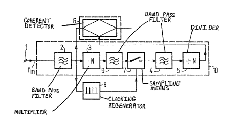
Figure 1: shows a bloc~ diagram of a receiver
3~
,
PHN 11.972 3 11.03.1987
comprising a carrier reproducing circuit for continuous
phase-modulated signals having a rational modulation
index in accordance with the invention,
Figure 2a: shows the impulse response and
Figure 2b: shows the waveform of a 2~C-signal,
Figure 3a: shows the impulse response and
Figure 3b: shows the waveform for CORPSK (2-3,
1 + D) and duebinary CP~I with h =
O,5 and
Figure 4a: shows the impulse response and
Figure 4b: shows the waveform for TFM and TFSK,
respectivelyO
With the receiver comprising a carrier-repro-
ducing circuit 10, shown in Figure l, it is possible
15 to extract in a highly reliable way a continuous phase-
modulated carrier signal (CPM-signal) applied to input-
terminal 1 and having a rational modulation index h
such that the resulting carrier has a small phase jitter.
Before embarking on the explanation of the carrier re-
producing circuit, the struc-ture of such a CPM-signal
is further elucidated.
An information signal to be -transferred digital-
ly, represented by a series (am) of m-nary digi-tal
symbols,
25 (a ) = .. a 2,a_1~ao'al'a2~ n (1)
with am = ~(2n~1) and n=0,1,2,...etc.
can be represented as a function of time by
a(t) = ~ amp(t-mT~ (2)
with T represen-ting the duration of the digital symbols
and p(t) representing a rectangular pulse of a length
of T.
Before transferring such signals they are pre-
ferably modulated in that the modulated carrier signal
has a constant amplitude. The major advantage of such
a carrier signal is the fact that non-linear signal
processing such as non-linear amplification for obtaining
a high efficiency, can be used without affecting -the
information contained in the signal
3~,~3(3
PHN 11.972 1~ 11.03,1987
Each digital modula-tion having a cons-tant ampli-
tude can be written as:
u(t) = cos(~ct + ~(t)) (3)
wherein ~c represents the angular frequency of the
carrier signal and ~(t) represents the phase as a
function of time.
If ~ ~t) is varied as a function of a(-t)
the following equation will be obtained:
~(t) ~ ~{a(t)) (4)
In Phase Shift Keying (PSK) ~ (t) is kept
constant over the symbol time T and changed abruptly
at the symbol transitions.
However, there are also types of modulation
such as Continuous Phase Frequency Shif-t Keying (CPFSK),
for which the following condition holds:
d ~ (t)/d(t) = K-a(t) (5)
wherein K is a constant. With Con-tinuous Phase Fre
quency Shift Keying the detection process for obtaining
a better S/N ra-tio can be spread out over more than one
symbol interval.
Examples of CPFSK are Minimum Shift Keying
(MSK) and Sinusoidal Frequency Shift Keying (SFSK). MSK
is a modulation entailing a linear phase shift o~`
~ ~/2 per symbol time, which is denoted by the modu-
-
lation index h = O.5 wi-th h being defined as -the number
-
of ~ radians which the phase is changed per symbol
time T.
With SFSK not only the phase but also the
first derivative of the phase, so the frequency, is
continous. This improves side-band suppression.
I~ the phase shift with CPFSK is made such
that smooth phase transitions between s~mbol inter-
vals are realized, the phase change will no longer be
constant over a symbol interval and one will commonly
refer thereto as Continuous Phase Modulation (CPM).
In view of the ever occurring phase changes over each
symbol time, a special carrier reproducing circuit,
for example as shown in Figure 1~ has -to be used for
~ ~ ~t~3 ~
PHN 11.972 5 11.03.1987
extracting the carrier signal from a received CPM-signal.
Examples of CPMs are Raised Cosine Modula-tion
(RCM), having a self-explanatory name and the category
of Correlative Phase Modulation (CORPM).
To achieve a further smoothing of the phase
shift when using CORPM, the phase change in a symbol
time also depends on the information of one or a
plurality of preceding symbol times. Known CORPMs are
the Tamed Frequency Modulation (TFM), Correlative
Phass Shift Keying (CORPSK) and Gaussian Modified
Shift Keying (GMSK).
Of all CPM-types only those types are of im-
portance to the invention wherein at fixed points of
time substantially fixed phase values occur which can
15 be denoted as a whole fraction of 2 ~ , for example
2 ~ /2 with n = ~ 2,
These types of modulations will further be
indicated as CPM with a rational modulation index h.
If a carrier signal modulated thus is applied to
input terminal 1 of the receiver comprising the carrier-
reproducing circuit 10 represented in ~igure 1, thesignal is applied to a multiplier 3 in the conventional
manner after being ~iltered in a band-pass filter 2
which will further be referred to as a -third bandpass
filter. Such a multiplier 3 comprises a non~linear
elemen-t by means of which the modulated carrier signal,
having a factor M and preferably being equal to 2/h,
is multiplied for achieving a desired harmonic. ~s a
result of the multiplication the phase variations of
the modulated carrier signal end up in the same phase
(modulo 2 ~ ). In known carrier-reproducing circuits
for CPM modulated signals the thus obtained signal is
directly applied to a first bandpass filter 4 having
a small bandwidth, for example in the order of 1/1oOth
fIN, where fIN represents the frequency of the received
signal, for elimina-ting all undesired harmonics, after
which the desired harmonic of the carrier signal is
divided in a divider 5 having dividend N. The thus
73~
PH\ 1 .972 6 11~03.1987
reproduced carrier signal is applied to a coherent
detector 6 likewise connected to the third wide-band
filter 2 for coherent demodulation of the filtered
input signal.
Figures 2a to 4b show several examples of
CPM-signals having a substantially rational modulation
index. Figure 2a shows therein the impulse response
g(t) of a pulse applied to a modulator (not shown) in
a transmitter for RC-signals. The time is plotted along
the horizontal axis in units of the symbol time T and
the amplitude is plotted along the vertical axis in
units of ~ . This Figure shows that the impulse res-
ponse for RC-modulated signals repr.esented therein
has a length of 2T and is therefore a CORPM-signal
indicated by 2RC. Figure 2b depicts in a waveform the
phase shift of a carrier signal continuously phase-
modulated by means of this impulse response. Such a
waveform represents any occurring phase variations as
a function of time of a carrier signal modulated by
an arbitrary data signal. Along the vertical axis
is plotted the phase in units of whereas along the
horizontal axis the time is plotted in units of symbol
time T.
As is shown in these Figures the phase at the
instants mT, with m = O, 1, 2, ..., has a specific
value equal to Gne of the values nH~ , with n = O,
+ 1, + 2, ... etc. The fact that the phase substantially
has fixed values at the afore mentioned instants is
caused by the surface under the impulse response curve
g(t) and hence the modulation index having the value
equal to h due to -the dimensioning of the premodulation
filter, so that the phase per -time T can exactly change
by the values of h ~r . In most types of CPM modulation
the phases at the instants mT have the constant unique
values of (O + 2 ~ n) only after multiplication of the
modulated carrier signal by -the factor 2/h in the mul-
tiplier 3. An example of an exception to this is formed
by TFM, wherein a substantially constant unique value
PHN 11.972 7 11.03.1987
((+2n~ r ) occurs not only with a fac-tor eight but
also with a factor four, as will be explained herein-
after t
Figure 3a shows the impulse responses g(t) and
Figure 3b shows the relevant waveform for CORPSX (2-3,
1+~) in solid lines and for duobinary CPM in dashed
lines. In the indication (2-3, 1~D) the numeral 2 points
out that the information signal applied to the premodu-
lation filter is binary, the numeral 3 that the output
signal of the premodulation filter is trinary for modu~
lating the carrier signal wi-th three different phase
values, and 1+D -that the successive information bits
are correlated because in the premodulation filter the
instantaneous standardized information bit, indicated
by 1, has to be added to the preceding information
bit delayed over a period time T indicated by the D
of DelayO
In Figure 3a the area underneath the impulse
response curve g(t) has the value of 1/2 so that all
branches of the waveform pass through the fixed phase
points n ~/2 at the instants nT. Multiplication in
multiplier 3 (Figure 1) by 2/h = 4 brings the phase
at the~forementioned instants back to O + 2 ~ n in the
desired harmonic.
As a last example Figure 4a shows the impulse
response g(t) and Figure 4b shows the associated wave-
form for TFM in solid lines whilst for TFSK (Tamed
Frequency Shift Keying) the dashed lines are used~
Here too the phase of the carrier signal turns out to
have exact values at the end of the symbol intervals,
in this case equal to n ~/4. Consequently, a multipli-
cation by a factor 8 is required in the multiplier
(Figure 1). However, Figure 4b shows that in the centre
of the symbol intervals the phases always turn out to
be close to the values of ~/4 + n ~/2, where n is an
integer. Multiplying this signal by a factor 4 in the
multiplier 3 will now suffice for achieving the sub~an-
tially fixed values ~ ~ 2 ~ n at the aforementioned
3~;~3V
PHN 1l.972 8 11.03.1987
sampling points (1/2 + m)T in the desired harmonic sig-
nal.
Despite the fact that the phases at the afore-
mentioned sampling points do not exactly have the
values of ~/4 + n ~ /2, with respect to the fixed
phase points at the sampling points mT, this is advan-
tageous in that a reliable carrier reproduction is
feasible by a mere multiplication by a factor L~.
For CPM-signals having a rational modulation
index it may be concluded from the aforeshown examples
that by a multiplication by an integer the phases of
the carrier signal are incremented such that at cer-
tain sampling points a single vir-tually fixed phase
value occurs in the desired harmonic signal, ~or
example O + 2 ~ n or ~ 2 ~ n, that is to say a carrier
phase irrespective of the symbol pattern of a data series.
Extracting the carrier signal by supplying
the output signal of the multiplier 3 directly to the
narrow-band first bandpass filter 4 in the conventional
way, has a sub-optimal result due to the not insigni-
ficant jittor in the reproduced carrier signal. This
jitter effect occurs as mary elements causing distur-
bance occur in the signal after the multiplier 3 in
addition to the desired phase values at the aforesaid
sampling points.
To reduce this jitter e,fect the carrier repro-
ducing circuit 10 comprises a sampling means 7 inserted
between the multiplier 3 and the first bandpass fil-ter
4, which sampling means is controlled by a clock signal
coming from a clock signal regenerator 8. This clock
signal regenerator 8 is connected to the wide band
filter 2 for regenerating an accurate clock signal in
the known manner from tne signal produced by the wide
band filter 2. Such a clock signal regenerator is, for
example, described in the aforementioned article en-
titled "Synchronization properties of continuous phase
modulation'l by T. Aulin and C.E. Sundberg, published
in the Conference Papers of Globecom 82, Global Tele-
~ ~7~
PHN 11.972 9 11.03.1~87
communications Conference, Miami, 29 November - 2
December 1982.
The clock signal regenerator 8 further com-
prises a delay means, which is not shown, (for example
a delay line) having such a delay that the delayed clock
pulses occur at the sampling point desired for a spe-
cific CPM signal in each symbol interval. If the re-
ceiver has to be suitable for receiving several types
of CPM signals, a single adjustable delay means can
be used to advantage rather than several switchable
delay means.
As the phase of the modulated carrier signal
has the desired value only at one or in some cases at
two points per symbol interval, it is essential that
the phase be sampled only at these points. This implies
that sampling by means of a sampling pulse wider than
an instantaneous sampling pulse will have a detrimental
effect on the accuracy of the reproduced carrier sig-
nal.
A further improvement is obtained by inserting
a relatively wide second bandpass filter 9, preferably
having a bandwidth in the order of fIN, between the
multiplier 3 and the sampling means 7, to isola-te the
spectrum of the desired harmonic.
The improvement of a single C.P.M. signal
having a rational modulation index, more specifically
a TFM-signal, achieved by sampling will now further
be explained with reference to a table showing computer
simulations.
In the first column of the table is shown the
S/N-ratio of the TFM-signal applied to the reproducing
circuit of Figure 1.
The three remaining columns of the table show
the square root of the mean square value of the phase
error ~ 0 of the reproduced carrier signal over the
last 136 da-ta symbols of 156 received data symbols as
well as the acquisition time TaCq of the receiver, ex-
~ ~73~
PHN 11.972 10 11.03.1987
pressed in symbol times T, assuming acquisition if thephase error is smaller than 5 . More specifically,
the first column of these three shows the aforementioned
values for a multiplication factor N=4, without sampling
the second column shows the values for a multiplication
factor N=4 with instantaneous sampling in the centre
of the symbol intervals and the third column shows
the valu~s-for a multiplication factor N=8 with instan-
taneous sampling at the end of the symbol intervals.
_ - _
S/N ~ 0rms(deg)/Tacq(symbols)
(dB) wi-thout sampling with sampling with sampling
N=4 N=4 N=8
_ . ~ .
1540 0.5/7 0.5/3 0.1/5
16 1.6/2 -I.~/6 0.6/2
13 2.~/3 1.4/5 1.1/2
3.6/10 1.9/7 6.3/7
7 4.9/12 3.3/~
Table fvr TFM signal
From this table it can be concluded that with ins-tan-
taneous sampling in -the cen-tre of the bit interval (N=4)
a considerable improvement in suppressing phase jitter
is achieved for TFM-signals compared with the cases
where no sampling is used. More specifically so with
S/~ ratios which are most important in practice. At a
S/N-ratio of 10 dB, for example, the improved phase
jitter suppression is even 6 dB. With instantaneous
sampling at the end (N=8) of the symbol intervals, where
the phase is exactly equal to a multiple of ~/4 9
the jitter suppression is far better than with instan
taneous sampling in the centre (N=4) of -the symbol
intervals, more specifically, up to a S/N ratio better
than approximately 12 dB. However, at a S/N ratio of
10 dB the high multiplication factor starts taking i-ts
toll and the phase jitter in the reproduced carrier
signal will rise rapidly.
73~
PHN 11.972 11 11.03.1987
Indeed, for prac-tical values of the S/N ratio
the multiplication factor 4 with centre-sampling is to
be preferred. The above-mentioned example will have
shown that improvements similar to those shown for
TFM signals will likewise occur for other CPM-signals
having a rational modula-tlon index.