Note: Descriptions are shown in the official language in which they were submitted.
:~L2~7~
--1--
Description
Low Voltage Swin~_CMOS Receiver Circuit
Technical Field
This invention relates to integrated semiconductor
circuits and more particularly to complementary
metal oxide semiconductor (CMOS) or complementary
field effect transistor (FET) circuits which
receive input signals from circuits having low
voltage levels or swings.
Background_Art
.
Integrated semiconductor receiver or buffer
circuits having low voltage input levels or
swings, such as outputs from bipolar circuits, are
~ known in the prior art.
: ~
U. S. Patent 4,438,352, filed on August 17,
1982, by M. M. Mardkha discloses a
transistor-transistor logic [TTL) compatible CMOS
input buffer which includes an input terminal
connected to yate electrodes of a series circuit
; 20 having first and second P channel transistors and :
: .~;: . - . .
a first N channel transistor and a second N
channel transistor connected in parallel with the
second P channel transistor, the output terminal
being the common point between the first N channel
transistor and the second P channel transistor.
Other examples of T~L to CMOS input buffers
or level shift circuits include U. S. Patent
4,258,272, filed on March 19, 1979, by J. Y.
Huang, U. S. Patent 4,295,065, filed on August 13,
. ~ . ,,
BU9-8$-026
~2~1)01
1979, by P. K. Hsieh et al and U. S. Patent
4,475,050, filed on May 5, 1983 by G. F~ Noufer.
Also, U. S. Patent 4,031,409 filed on May
26, 1976, by S. Shimada et al discloses a circuit
~or converting a binary signal from a bipolar
transistor logic circuit to the levels required
for binary signals by insulated gate field effect
transistor circuits.
An emitter coupled logic ~ECL3 compatible
CMOS circuit is disclosed in U. S. Patent
4,437,171, filed January 7, 1982, by E. L. Hudson
et al.
Interfacing CMOS circuits to bipolar
technologies poses some difficulties because the
bipolar signal level changes or swings are much
smaller than that which is required for the
operation of the normal CMOS circuit. A CMOS
circuit havlng a normal 5 volt power supply is
generally optimized to switch its transistor
elements at approximated 2~5 volts. However,
known circuits in the bipolar technology have,
e.g., the least positive up level of 1.5 volts and
the least negative down level of 0.6 volts. Other
bipolar circuits, e,g., the TTL circuits~ have
corresponding levels of 2 volts and 0.8 volts. It
can be seen that the output voltages from these
bipolar circuits cannot be readily used to switch
the normal CMOS circuits. 9y modifying the
dimensions of the N channel and P channel devices
of the CMOS circuits, the center of the switching
point can be shifted, however, the variations due
to power supply and process parameters remain
intolerably large.
BU9-85-026
~;~7~
Disclosure of the Invention
It is an object of this invention to provide
an improved, simple CMOS receiver circuit for low
input voltage levels or swings which has high
performance, hiyh density and low, and under
certain conditions 0, power dissipation.
In accordance with the teachings of this
invention, an improved simple CMOS receiver or
buffer circuit is provided which includes a first
inverter having its output connected to the input
of a second inverter with means connected in
parallel with the first inverter to initiate a
more rapid switching action in the first inverter
at low input voltage swings.
More specifically, the CMOS receiver or buffer
circuit includes a first series circuit having
first and second P channel devices and a first N
channel device with an input terminal connected to
the control electrode of each of the devices and a
second series circuit connected across the first P
channel and first N channel devices, with an
output terminal located at the common point
bet~een the first P channel 'device and the~first N
' channel device.
The foregoing and other ob~ects, features and
advantages of the invention will be apparent from
the following and more particular description of
the preferxed embodiments of the invention,,as
illustrated in the accompanying drawings.
BU9-85-026
~2~4~3~
Brief Description of the Drawin~s
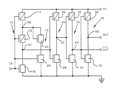
Fig. l illustrates an embodiment of the
receiver or buffer circuit of the present
invention,
Fig. 2 is a graph of the voltages versus time
at selected points in the circuit of Fig. l when a
full input swing is applied to the input terminal,
Fig. 3 is a graph of the voltages versus time
at selected points in the circuit of Fig. l when a
voltage input swing substantially smaller than the
e~pected full input swing is received, and
Fig. 4 is a graph indicating the transfer
characteristics of the receiver or buffer circuit
of Fig. l.
Best Mode for Carrying Out the Invention
Referring to the drawings in more detail,
there is illustrated in Fig. l the CMOS receiver
or buffer circuit of the present invention which
includes a first series circuit l0 having first
and second P channel transistors l2 and l4,
', :, . , r .
respectively, and a first N channel transist~r ~6
and a second series circuit 18 having second and
third N channel transistors 20 and 22,
respectively, with the third N channel transistor
22 connected as a diode. The ~irst series circuit
l0, with an output node or terminal Nl, is
connected between a voltage supply terminal V~I and
a point of reference potential, such as ground,
and the second series circuit 18 is connected from
the common point N2 between the first and second P
BU9-85-026
74~
5--
channel transistors, 12 and 14, respectively, and
ground. Transistors 12 and 16 of the first series
circuit 10 act as an inverter. An input terminal
IN is connected to the control electrodes of the
first and second P channel transistors 12 and 14,
respectively, and of the first N channel
transistor 16, as well as to the control electrode
of the third N channel transistor 20.
The circuit of Fig. l further includes a
first inverter 24 having a third P channel
transistor 26 and a fourth N channel transistor 28
wi.th output node or terminal N3 located at the
drains thereof. The gate electrodes of the third
P channel transistor 26 and the fourth N channel
transistor 28 are connected to the output terminal
N1 of the first series circuit 10. A second
inverter 30 has a fourth P channel transistor 32,
a fifth N channel transistor 34 and an output
terminal N4, with its input connected to the
output terminal N3 of the first inverter 24. A
third inverter 36 has a fifth P channel transistor
38, a sixth N channel transistor 40 and an output
terminal N5, with its input connected to the
output terminal N4 of the second inverter 30. A
true output signal ~rom the circuit of Fig. 1 is
;~ provided at its outpUt terminal ~UT connected to
the output terminal N5 o~ the third inverter 36
and a complement output signal from the circuit of
Fig. l is provided at its output terminal OUT
connected to the output terminal N4 oE the second
inverter 30.
The P channel transistor 14 of the first
series circuit is a current source whose value is
a function of the input voltage IN and power
BU9-8S-026
~2 7~Q~
--6--
supply voltage ~TH, as well as the voltage at node
N2. The transistor 22, connected as a diode,
provides a process-dependent voltage offset from
the drain of N channel transistor 20. The P
channel transistor 12 is a current source whose
value is a function of the input voltage IN and
the conduction states of transistors 14, 20 and
22. Transistor 12 governs the amount of current
that must be switched by the N channel transistor
16, and, as such~ sets the switching point of the
receiver circuit, i.e., when node Nl goes from a
high voltage to a low voltage, or vice versa. The
N channel transistor 16 is a switching
device with its dimensions relative to the current
lS generated by the P channel transistor 12
determining the value of the input voltage IN at
which switching occurs in the receiver circuit.
The N channel transistor 20 is a current source
whose value depends on the input voltage.
Transistor 20 is turned off completely at
substantially low input voltages. Transistor 20,
together with transistors 14 and 22, determines
the source voltage of transistor 12, which, in
turn, effects the current through transistor 12
and influences the switching point of the receiver
circuit. For the up levels of the input voltages,
; transistor 12 turns off completely. The ~ ;-
dimensions o~ the P channel transistor 26 and N
channel transistor 28 of the first inverter 24 are
selected to translate the switching point of the
input stage of the receiver circuit to the optimal
value for the subsequent inverter, buffer or
amplifier stages 30 and 36. The correct selection
of the dimensions of transistors 26 and 28 results
in symmetric delay characteristics in the circuit.
BU9-85-026
~274~01
--7--
The operation of the receiver or buffer
circuit of Fig. 1 of the present invention may be
better understood by referring to the graph of the
voltages versus time at nodes or terminals IN, Nl,
N2, and N3 as shown in Fig. 2 of the drawings.
With the voltage supply terminal VH being at, say,
+5 volts and the input voltage at terminal IN
being at +0.4 volts at time 0, the voltages at N1
and N2 are at +5 volts since P channel transistors
12 and 14 are turned on and transistors 16 and 20
are turned off, at this point the power
dissipation being 0. With N1 being at +5 volts,
the output voltage at N3 is 0 volts since
transistor 28 is turned on and transistor 26 is
off. At time 10 nanoseconds (ns), when the input
voltage at IN begins to increase to about +2.4
volts, the voltage at N2 begins to decrease
rapidly to about +1.8 volts, du~ to transistor 20
turning on. During the transition period, when
the voltage at IN is increasing and the voltage at
node N2 is decreasing, a point is reached at which
P channel transistor 12 is turned off completely,
allowing N channel transistor 16 to freely
discharge node Nl. The decrease in voltage at N1
causes the output of the first inverter 24 to
switch rapidly fxom 0 volts to the full supply
voltage of ~5 volts within several nanoseconas.~ `- -
At time 20 ns, the input voltage IN is at its peak
value of +2.4 volts, Nl is at n volts r N2 is at
+1.8 volts and N3 at +5 volts. The input voltage
IN between +0.4 and ~2.4 volts may be considered
as a full voltage swing from TTL bipolar circuits.
As indicated in the graph of Fig. 2 ~ the
voltages at IN ~ Nl r N2 r and N3 remain constant
3s from time 20 ns to 50 ns when at 50 ns the input
voltage IN is decreased toward ~0.4 volts causing
BU9-85-026
.. . ~ ... .
~;Z'7~
the voltage at N2 to rapidly increase toward ~5
volts with the voltage at Nl increasing even more
rapidly to ~5 volts, while the voltage at N3
decreases to 0 volts. At time 60 ns, the voltages
at INI N1, N2, and M3 are at the same values as
they were ~rom time 0 to 10 ns. Although not
indicated in the graph of Fig. 2, the voltage at
the output terminal N4 of the second inverter 30
i5 the complement of the voltage at the output
terminal N3 of the first inverter 24, i.e., when
the voltage at N3 is high to indicate, e.g., a 1
binary digit of information, the voltage at the
output terminal N4 is low to indicate a 0 binary
digit. The voltage at N5 of the third inverter 36
corresponds to the voltage at N3 which represents
the true output signal or voltage at terminal OUT
of the receiver circuit of Fig. 1, while the
volta~e at N4 of the second inverter 30 represents
the complement output signal or voltage at
terminal O~T of the receiver circuit of Fig. 1.
It should be noted that the receiver circuit
of the present invention as illustrated in Fig. l
of the drawings can operate successfully with an
input voltage swing significantly smaller than
tha~ indicated by the graph of Fig. 2. For` ~
example, as indicated in-Fig. 3 of the drawings, ;- -
the input voltage swing at input ter~inal IN can
extend only between about ~1.1 and +1.7 volts to
successfully operate this circuit. With the input
voltage at terminal IN at ~1.1 volts, while the
supply voltage VH is at ~5 volts, N channel
transistors 16 and 20 are slightly on with the P
channel transistors 12 and 14 being substantially
on. Thus, due to voltage drops through P channel
transistors 12 and 14, the voltage at N1 is at
BU9-85-026
~LZ7~
_9_
about 3.7 volts and at N2 is at about 4,2 volts,
with N3 being near 0 volts, since the N c~annel
transistor 28 of the first inverter 24 conducts
substantially more than does the P channel
transistor 26. When at 10 ns the input voltage IN
begins to increase toward ~1.7 volts, the voltage
at N2 begins to fall to about -~2.6 volts and the
voltage at Nl begins to fall more rapidly toward 0
volts since the N channel transistors 16 and 20
conduct more heavily and the P channel transistor
12 is fully turned off. The voltage at N3 of
inverter 24 thus rises rapidly from 0 to +5 volts
since transistor 28 turns off and transistor 26 is
turned further on. At time 50 ns the input
voltage IN begins to decrease from +1.7 volts to
~1.1 volts reducing the conduction of N channel
transistor 16 and turning on P channel transistor
12, causing the voltages at Nl and N2 to return to
+3.7 and ~4.2 volts, respectively, and at N3 to
~0 return to 0 volts.
It should be understood that device or
transistor parameters of the circuit must be
suitably adjusted as is known so that current in
the P channel transistors 12 and 14 and the N
channel transistors 16 and 2`~ are appropriàtely
. .,.,, ~ .
controlled by the small inPut voltage swing IN - -
indicated in Fig. 3 of the drawings for the entire
range of expected power supply voltages and
process parameters.
In Fig. 4 there is shown a graph of the
composite transfer characteristics of the receiver
circuit of E'ig. 1 for an expected range of power
supply voltage, temperature and process parameter
variations. It can be seen that when the voltage
BU9-85~0Z6
' .
1;~ 7 4 ~
-10-
at .input terminal IN increases to above -~1.3, the
voltage at the output terminal OUT always
increases to VH and when the voltage at the input
terminal IN is reduced below ~.9 volt, the voltage
at the output terminal OUT always decreases to 0
volts.
It should be noted that appropriate
modifications may be made to the circuit of Fig. 1
by those skilled in the art, if desired, e.g.,
transistor 22 may be formed as a conventional
simple PN junction or as a resistive impedance.
Furthermore, if desired, the control electrode of
N channel transistor 20 of the second series
circuit 18 may be connected to any appropriate
point of reference potential in the range of 0 to
VH volts~ which may be constant or variable under
external stimulation such as temperature, process
conditions, etc. Also, various improvements of
this circuit may be realized by utilizing
appropriate known feedback techniques. Still
another embodiment of the invention may be made by
reversing the polarities of the transistors, as
well as the ground and VH connections of the first
serie$ circuit 10 and the second seri.es circuit
2S 18, to use the circuit for dëtecting a small .
signal swing with ref.erence to V~
Although relatively low input voltage swings
have been discussed hereinabove in connection with
the operation of this receiver circuit, it should
also be noted that input voltage swings from VH to
ground may be used, if desired~
BU9-85-026
. .
l;Z~r74LO~ l.
While the invention has been particularly
shown and described with reference to preferred
embodiments thereof, it will be understood by
those skilled in the art that various changes in
form and details may be made therein without
departing from the spirit and scope of the invention.
.,;
BU9-85-026
; . :