Note: Descriptions are shown in the official language in which they were submitted.
~2~
Thi3 invention relates to photoconductor~ in general and in par--
ticular photoconductive devices made of semiconductive material and
having a depleted channel layer.
Background of the Present Inventlon
Photoconductors made from epltaxial layers of CaAs or related
semiconductor compounds have shown considerable promise as detectors for
optical communications and as optoelectronic crosspoint switches. As
switches, they provide over 60 dB isolation, l GHz bandwidth, low
switching bias and subnanosecond switching time. (see Optical Engineer-
ing, Vol. 24, p.p. 220 - 224, 1985, "Optoelectronic Switch Matrices:
~ecent Developments" by R. I. MacDonald et al~. As detectors in an
optical communication link, they offer commensurate responsivity and
bandwidth similar to the more common P-N and P~I-N photodiodes. The
planar structures employed in the photoconductor fabrication allow ease
o~ monolithic integration. A large area epitaxial photoconductive
detector was reported in an article, "An epitaxial Photoconductive
Detector ~or High Speed Optical Detection", Proc. IEDM, 1979 p.p. 634-637
by J. C. Gammel et al. The photoconductive detector reported thereln
has an n+, p-, n+ structure which is used under bias conditions similar
to a punched-through transistor. The injection boundary conditions cause
the p- epitaxial layer to behave as a photoconductor, thus providing high
speed photoconductive gain.
Photoconductors can be made in interdigitated configurations to
preserve the short channel lengths necessary for high optical speed and
gain, and yet give relatively large active areas for ease of optical
coupling and low capacitance. Thus, C. Y. Chen et al report a heter-
ostructure interdigitated photoconductive detector in "Interdigitated
o.4~ InO 52 As/CaO 47 InO 53 As Photoconductive Detectors",
Applied Physics Letters, Vol. 44, No. 1, Jan. 1, 1984, p.p. 99-101.
Their detector shows a rise time of 80 ps, a ~all time of 1.2 ns and a
peak responsivity seven times better than that o~ a commercial PIN
photodiode. An artlcle entitled "On the Responsive Behaviour
., . . :
' . . '
J ~
1 o~ ~ast PhotoconductLve Optlcal Planar and Coaxia:l Sernlcotl(Juctor
Detectors" by 11. Benekir1~, IEEE Trans. on Electron Devices, Vol ED -
29, No. 9, Sept. 19a2, p.p. 1ll31-1441, reviews fast optical detectors,
which use photoconductive ef~ects, in semiconducting channe]s or thin
films.
The major disadvantage o~ most epitaxial photoconductors is their
large bias current, which can be o~ the order of tens of mA at operating
bias voltages of 10V. The di~iculty in making low-current CaAs photo--
conductors, for example, is that the resistivity o~ conventionally
prepared, undoped epitaxial material is typically a few ohm-cm while the
absorptlon length o~ the light to be detected is of the order of 1 ~m.
In consequence, the sheet resistivity o~ epitaxial photoconductive layers
suitable for efficient photoconductors is 10 - 30 kQ per square.
When interdigitated photoconductor configurations (aspect ratio
of less than 10-Z) are used to achieve the narrow channel length required
for significant photoconductive gain (less than about 10 ~m) simultan-
eously with a large photosensitive area of about 100 ~m square, the
channel width is correspondingly large resulting in a resistance of a few
. Z
~ ~ hundreds ohms, and the dark current is usually of the order of a ~
milliamperes. Such high currents contribute to the detector noise and
also cause an undesirable shift in the output level when the device is
used as an optoelectronic crosspoint switch.
To avoid this problem photoconductors fabricated directly in
Cr-compensated semi-insulating gallium arsenide have been reported in
"Frequenc~ and Pulse Response of a Novel Hi~h Speed Interdigital Surface
Photoconductor (IDPC)" by C. W. Slayman et al, IEEE Electron Device
Letters, Vol. EDL-2, No. 5, May 1981, p.p. 112-114. Cr dopants lntro-
duce electron traps that remove free carriers. These photoconductors
~r
exhibit very low bias currents (10~A at 20~f bias). However the high
density of deep traps shortens the lifetime of photogenerated carriers
and the photoconductive gain ls sacrificed.
United States Patent 4,490,709, Dec. 5, 1984 Hammond et al des-
cribes an InP:Fe photoconductive device. Instèad of GaAs doped with Cr
-
~`,. "' ' ' ;
:: ' .
in the above~referenced artlcle hy Slayman et al, Hammond et al u~e InP
doped with Fe as a semL-in3ulating ~emiconductive material. ~etal con-
tact~ are directly deposited on the Fe doped InP. Similar result3 to
those obtained by Slayman et al are given in the patent.
Objects o~ the i~vention
It is therefore an object of the present invention to pro-
vide GaAs or other ~imilar semiconductor photoconductive detector~
having low noise.
It is another object of the present invention to provide
photoconductive detectors which can operate with low bias current.
It i9 still another object of the pre3ent invention to pro-
vide photoconductive detectors which pos3es3 improved uniformity of
frequency response.
Summary of the_Invention
Briefly stated, a photoconductive device of the present in-
vention consists of an in~ulating or semi-insulating 3ub~trate on which
i8 provided a channel layer of a 3emiconductive material which is un-
doped, low doped or compensated. The device further includes a pair of
mutually separate metal contact electrodes on the channel`layer. The
said channel layer is thin enough that the depletion region created in
the channel layer between the electrode3 penetrats3 into the 3ubstrate.
Photons are directed to impinge upon the channel layer to generate a
photocurrent between the electrode~.
Bri~:iF De~scriDtion o~ th~3 Drawinc~s
For a more complete understanding of the present invention
and for further objects and advantages thereof, reference may now be
made to the following description taken in conjunction with the accom-
panying drawing~ in which:
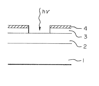
Figure 1 iY a cross sectional view showing the configuration
o~ the photoconductive device according to the present invention.
Figure 2 i9 a graph showing the re3ponsivity measured on a
device fabricated according to the present invention.
''' , '~ ': ~ ~ "
.:
,,, ::- ~
:..... ::: : :
~z~
1 Flgure 3 shows the bLas current and the nolse equLvalent power
characteristlcs o~ such a device a3 a ~unctlon of the applied bias vol-
tage.
Figure 4 i9 a photograph showing the isolation values measured on
the device o~ the present invention.
Detailed Descrlption of the Preferred Embodlment Or the Pre~ent Inventlon
The epitaxial structure of the present invention is shown in
Flgure 1. A semi inslllatlng or insulating substrate is deslgnated by 1
on which a channel layer 2 is grown. A cap layer 3 is grown on the chan-
nel layer to ensure a good ohmic contact between the channel layer 2 and
metal contact electodes ~. While other methods are possible, the photo-
conductor shown in Figure 1 i9 fabricated by the following process. The
channel layer 2 of unintentionally doped CaAs (n~= 5 x 1014 cm~3) is
grown by organo-metallic chemical vapour deposition (OMCVD) directly on
an undoped serni-insulating substrate 1 to a nominal thickness o~
1 - 2 ~m. The undoped channel layer is overgrown with a cap layer
(0.25 - 0.35 ~m, n~ = 2 x 10'~ cm~3) and a metal contact layer i9 formed
on the cap layer 3 with evaporated and annealed Ni-Ce-Au. The metal
contact layer is etched to form the electrode pattern and the cap layer
i9 removed between the metal contact electrodes. This latter process
step is performed with a calibrated etch (NH40H 2%, H2O2 0.7~, H2O 97.3%,
1500 A/min at 23C), and the resistance of the device is monitored at 30
second intervals. Etching is stopped when the resistance increases ~rom
a few hundred ohms into the Megohm region. This occurs when the etch
punctures the cap layer. The processes descri~ed are given by way of
example.s only and other well known etching processe~ are equally applic-
able to the present invention.
Since the undoped channel layer 2 is intact in this device, and
would ordinarily result in device resistance of a few hundred ohms, the
observed very high device resistance indicates that the ohannel i9
entirely depleted by surface effects. This is because the surface deple-
tion layer thickness for the low doped n~ layer is estimated to be a few
.
',: ''
~74~
1 microns t-hi~. The channel layer belng only 1 ~Im thlok re~3ults ln a
totally depleted channel, that is to ~ay, the depletlon reglon created ln
the channel layer between the electrodes penetrates lnto the substrate.
The optical response was observed by illuminating the photocon-
ductlve devices with a GaAlAs-CaAs laser diode with a wavelength of 820
nm and modulated at 400 MHz. The photoconductor has an overall dimension
of 100 ~m ~ 100 ~m interdigitated with 10 ~m finger~ spacing. The
responsivity of the photoconductor l~ shown in Flg 2. It inltlally
increases with voltage until it saturates at about 2 Volts. At this
voltage the internal electric field is sufficient to produce carrier
velocity saturation. The carrier velocity saturation limits the photo-
conductive gain which in turn limits the responsivity. The theoretical
responsivity i9 calculated as:
R neg
hv
where n - quantum efficiency
e = electronic charge
h = Planck's ~r~t
evn~tan
v = frequency
g = photoconductive gain
The quantum efficiency is compri~ed of the Fresnel reflection
coeffioient, the coverage of a portion of the active area by the metallic
interdigitated fingers, and the ab~orption o~ light ln the aotiYe chan-
nel. A quantum efficiency of 18% is estimated~ Substituting this into
~ the equation above and comparing the result with the experimental obser-
vation as shown in Fig. 2 indicate that a photoconductive gain of 2.5 is
present.
':,''~ :- . : : . :,
, . :. .. . ,. ;- , :
-: '.. ,...... ' ' "" '' :
~l~7~
- 6 -
1 The DC responsivity in these surface depleted photoconductors 13typically only a factor of 2 or 3 greater than the responsivity at RF
frequencies. This ratio is less than that observed in many other photo-
conductors and would ease considerably the problem of frequency equal-
ization in photoconductive receivers. The reduced difference between low
frequency and high frequency response is attributed to the reduction of
contributions from phototransistor-like actLon through optical modulation
of the channel width that occurs in structures that are incompletely
depleted. Since the channel is always completely depleted in these
devices, mechanisms such as optical back gating cannot modulate the
impedance o~ the device.
The experimental results o~ the bias current and the noise equi-
valent power (NEP) as a function of the applied bias as shown in Figure
~ 3. These measurements were taken on a photoconductor of ~
~" 20 ~m x 20 ~m. The bias current and the NEP at 4 volts bias are 17 nA
and 2.3 x 1o-l3 w/~Hz respectively. At this bias, the dark resistance is
about 240MQ. These values are considerably better than those of
conventional photoconductors and approach photodiode performance. Opera-
tion beyond 4V showed instability and a larger rate of increase in the
bias current and the NEP. This may be due to a high field e~fect such as
impact ionization
The depleted channel photoconductors of the present invention
were also evaluated as broadband optoelectronic crosspoints. Such cross-
points are used in switching matrices whereby broadband signals are
routed, distributed, or broadcast from a number of outputs. The signals
to be switched are introduced optically into the crosspoints. The
switching is accomplished by varying the bias applied to the crosspoints.
For photoconductors, the on and off conditions correspond to the biassed
and unbiassed conditions respectively. Photoconductors are most suitable
for switching operation because they possess very rast electrical
switching time and very high isolation values. These are the key para-
meters in the development of practical switching systems. Switching time
:
. :. ~ .
... :. :
1 and l~qolatlon are Inclependerlt parameter~ in photoconduotor~ but not inother semiconcluctor swltches. For ln~tance, a f`orward blas 1B requlred
in a photodlode Ln order to achieve hlgh isolatlon. This lntroduces
storage charge whlch in turn results ln a slow turn-on time, Switching
time and lsolation are therefore related in a conflicting manner in
photodiodes.
The i~olation value of a typical depleted channel photoconductor
i9 shown in Figure ~i. The upper trace shows the frequency response of
the channel depleted photoconductor mounted on a mlcrostrlp line circuit
bia~sed at 4V. The response is very ~lat to ~1.3 G~lz. (The cutoff below
300 MHz is due to a high pass network in the laser driver), The lower
trace ~how3 a 60 dB reduction in response when the bias is not applied,
A particular advantage of these depleted channel devices as opto-
electronic switches i~ the reduced dc offset that results from the
reduced dc photoresponse as well as the low bias current.
The electrical switching time wa~ measured by introducing a
variable time delay between the laser and the bias pulses applied to the
photoconductor. The lead time required for the bias pulse with respect
to the laser pulse to acquire a 90% response from the photoconductor is
the turn-on time. In a similar fashion the time for the response to fall
to 10% is the turn-off time. The turn-on and the turn-off times for the
depleted channel photoconductor were measured to be 0.3 and 0,5 ns res-
pectively, the difference being mainly due to the asymmetry in the bias
pulse. Optoelectronic crosspoint switching spaeds offered by these dete-
Ctors are much faster than those offered by photodiodes.
As described above, the channel layer in the photoconductor~ of
the present lnvention i~ thinner than the suri'ace depletion layer pro-
duced at the GaAs-air interface. It is therefore possible to improve the
~ efficiency of the detector by matching the channel thic~ness more closely
to the depletion depth. It is also possible to fabricate the depleted
channel photoconductors of the present invention wlth semiconductive
3S
.. . ..
: ,, :
: . .:. : :
~2~7~
-- 8 --
I material other than Ca~s. For example, other Irl-V compounda, ~uch as
~i ~ ~J ~
InP, GaInAs or Si on ~ ~ e are examp]es o~ auch materlals. Configur~
at1ons other t~lan that shown in Figure 1 can be employed depending upon
materials used. For example, the cap layer shown in the figure can be
eliminated. Or on the other hand, the substrate may comprlse a second
buffer layer contacting the channel layer. This buf`fer layer may be made
o~ a di~f`erent material ~rom that o~ the remaining substrate or may be
made by doping a part o~ the substrate dirferently from the other part.
In conclusion the depleted channel photoconductors of the pre~ent
` invention have significantly reduced bias current, lower noise, and
f`latter frequency response than similar photoconductors made with doped
or undepleted channels. Their performance as optoelectronic crosspoint
switches is comparable or better than other photoconductors. A photo-
conductive gain of` 2.5, a dark current in the nanoampere region, a NEP of
the order oi~ 10-l3 w/~Hz, an isolation value o~ 60 dB over 1.3 GHz
bandwidth and an electrical switching~ time o~ 0.3 ns have been achieved.
These properties make the depleted layer photoconductors of` interest f`or
many optical co0munication applications. An additional f`eature of` these
devices is that their higher impedance permits a correspondingly higher
load resistor to be used, consistent with R-C time constant constraints,
in order to provide higi1er voltage outputs. The reduced bias current en-
sures that excessive bias power in not dissipated in the load resistor.
The latter dissipation can be signi~icant in large scale optoelectronic
switching applications.
; , - ___ _ _
.: .~ ': .: , -
'' -. :~
~,.. .