Note: Descriptions are shown in the official language in which they were submitted.
-- 1 --
PROGRAMMABLE INTERLACF WITH SKIP AND CONTRAST
ENHANCEMENT IN LONG PERSISTENCE_DISPLAY SYSTEMS
~ross-Reference to Relate _Application
This is a companion to related Canadian Patent
Application, Serial No. 520,790, filed October 17, 1986
by Cornelius J. Starkey, IV, and entitled "CRT Dlsplay
System with Automatic Alignment Employing Personality
Memory".
Ba~ground of the Invention
The present invention relates to image
generation techniques for electronic displays. More
particularly, the invention relates to programma~le
interlace with optional skipping of non-information
carrying lines in a raster-scanned display, to a related
contrast enhancement technique herein termed "rolling
writing'l, and to direct point writing techniques. While
techniques of tha invention are applicable to any long-
persistence display, the specific example disclosed in
detail herein is a cathodochromic CRT display, which has
an infinitely long persistence, until it is deliberately
erased.
Most CRT based display systems, as well as some
flat panel displays, use the raster scan technique of
image generation. Raster scan in a CRT
-
, . ... ..
`',' ~ - ,. :
:~ ,
:.'; . ~ . ' . -
.~ :
.
: ~: ~ ' :
-- 2 --
employs a scanning electron beam to write an image on
the phosphor-coated face of the CRT a line at a time
from top to bottom. In CRTs with short duration
phosphors, like a television set, this process is
repeated at fairly high rates, 30 to 60 times per
second. The high rate is needed to reduce flicker in
the image caused by the fading of the light emitted by
the relatively short persistence phosphor after it is
hit hy the scanninq electron beam. Longer duration
phosphers are not used in conventional television
because they would preclude motion in the generated -
image.
If all lines of the image are scanned
- sequentia:Lly in one pass from top to bottom, the
generated image by definition has a 1:1 interlace
ratio. If the image is generated in two passes, one
pass doing the odd lines and the other doing the even
lines, then by definition the generated image has a
2:1 interlace ratio. The entire generated image is
called a frame. If a 2:1 interlace, or higher~ is
used, each pass is called a field and the display must
show '`n" fields to make a complete frame, where 'ini' is
the interlace ra~io. Interlace is used to reduce
flicker by increasing the apparent refresh rate and
lower the bandwidth re~uirements of the display
electronics. U.S. standard television uses a 2:1
interlace. Interlace ratios higher than 2:1 are very
rarely used in displays, and 1:1 is used in most high
resolution applications.
In storage and long persistence displays
higher interlace factors can be useful. Since the
images used are static, a detailed high resolution
image can be generated at higher interlace factors
providing a low resolution image very quickly. The
image then becomes more detailed as the subsequent
fields are scanned.
: ~ .
. :. :
., ..:...
~ ;~'`,7~
-- 3 --
As noted above, while the invention is
applicable to any lonq-persistence display system, the
particular application described herein is a high
resolution cathodochromic CRT projection display
system. Accordingly, several characteristics of such
a display will now be summarized.
An image target on which an electron beam
impinges in a cathodochromic CRT does not emit light
as does an image target in a cathodoluminescent CRT.
Rather, the ca~hodochromic materials employed change
color when excited by an electron beam. In the case
of an image target comprising cathodochromic bromine
sodalite, the resultant coloration remains
indefinitely, until deliberately erased. In addition
to inherent memory, cathodochromic image targets have
the properties of high resolution, and high contrast
in bright ambient light making them highly suitable
for projection systems.
Erasure of a cathodochromic image target is
normally effected by heating to about 300C. An
economical and technically feasible erasure method is
electron beam heating, wherein the image target is
scanned, in a raster pa~tern, with an electron beam
spot energy density such that temperature is raised
above an erase threshold.
Processes for preparing cathodochromic
sodalite and a cathodochromic CRT projection display
are disclosed in Todd, Jr. et al U.S. Pat. No.
3,932,592 and Todd, Jr. U.S. Pat. No. 3,959,584 to
which reference may be had for further details.
Considering cathodochromic CRT display
characteristics in greater detail as they relate to
the present invention, the darkness of the black
pixels is a function of electron beam exposure time,
electron beam current level, and the temperature of
that pixel. The longer the exposure, the darker the
pixel gets, so long as the temperature of the
.
cathodochromic material at that pixel site remains
under the erase threshold temperature. A problem with
long exposure times is that the material is heated by
the electron beam to the point where it loses contrast
S (erases). This problem is exacerbated by the use of a
thermal insulation or buffer layer between the
sensitized cathodochromic material and the underlyinq
support, as is disclosed in the above-referenced Todd,
Jr. U.S. Pat. No. 3,959,584. The thermal buffer layer
aids in electron beam erasure, but does complicate the
writing process if good contrast is to be achieved.
Thus, multiple short exposures of a high current
electron beam separated by a relatively long coolinq
period are necessary for buildinq good contrast.
Typically, from 40 to 300 exposures per pixel may be
employed in a raster-scanned display before the final
contrast is achieved.
As a simple example, a 100 nanosecond
exposure with a delay of 100 milliseconds before the
next exposure is fairly typical. This provides a
cooling delay of 1,000,000 times the exposure time.
Carrying ~his example further, if the display
comprises 1,000 lines of 1,000 pixels each, a
conventional raster scan would ideally expose each
25 pixel once every 100 milliseconcls (1,000,000 pixels x
100 nanoseconds per pixel), giving a frame refresh
rate of 10 Hz (1/100 ms). Various system constraints,
however, could reduce the frame refresh rate to as low
as 3 Hz for such a high-resolution display.
This leads to a closely related problem,
known as flicker. A frame refresh rate of 10 Hz in a
display employing conventional (short persistence)
phosphor would have an unacceptably annoyinq flicker.
Interlace is commonly used to provide an acceptable
flicker level in a display system that has reduced
cost due to slower components, i.e. the horizontal
scan time is roughly doubled in qoinq to a 60 Hz field
. ' .
;~
: - .
7~
rate Erom a 60 Hz ~rame rate. This can greatly reduce
the display system cost and reduces overall system
bandwidth requirements, and also results in a 50%
(roughly) reduction in transmission spectrum space for
commercial TV over a 60 H% system. Typical displays
either sync or operate the field/frame rates at the
same (or multiple/sub multiple) as the power line
frequencey (60 Hz in the US) to reduce artifacts.
Such is the case with standard television, where each
o~ two alternating fields (odd numbered then even
numbered lines) is scanned at 60 Hz, yielding a 30 Hz
frame refresh rate and resulting in barely perceptable
flicker.
The manner in which these problems relate to
each other in a high resolution cathodochromic CRT
display will now be considered. As noted above, from
40 to 300 exposures per pixel may be required to build
contrast. Correspondingly, multiple complete frame
exposures allow the image to build contrast over an
interval measured in seconds. At the beginning of the
process of generating an image, particularly up until
the point where the contrast ratio is about 2:1, the
contribution to contrast of each successive frame
exposure is quite noticeable to the extent that even
an infinitely-lonq persistence cathodochromic CRT has
a perceptable flicker, much as a conventional phospher
CRT would have at the same frame rate~ In a
cathodochromic CRT, the flicker effect is manifested
in part as an annoyingly visible top to bottom
contrast enhancement.
Interlacing can also alleviate the flicker
problem in a cathodochromic CRT. With an interlace
ratio such that the resultant field rate approaches 30
~z, ~he contrast builds and an image gradually appears
much as the image on an "instant" photograph appears
as it develops.
.~
:
y ~.
4~
~,
Another advantage of interlacing is that the
heatin~ caused by thermal conduction ~rom adjacent
pixels on lines above and below occurs at least one
field time (rather than one line time) away, thus
reducing the peak ~emperature of the exposed pixels
allowing contrast to build faster and darker.
Interlacing alone does have its limitations
in a high resolution cathodochromic CRT display
system, due largely to the time required for a
complete scan. As a more particular example, in one
system in which the present invention is embodied,
there are a total of 2048 lines on the display, with
1728 pixels per line. At an exposure of 100
nanoseconds per pixel, multiplication gives an active
line time of 172.8 microseconds. Rounding this to 172
microseconds and adding a 10 microsecond horizontal
retrace time results in a total time of 180
microseconds per line. Multiplying again by the 2048
lines gives a frame period of 0.369 seconds, which
corresponds to a frame refresh rate of 2.7 Hz. This
figure is even worse when time for vertical retrace
and possible calculations during the vertical retrace
interval is taken into account.
To achieve a field refresh rate of 30 Hz
under these conditions would require an interlace
ratio of about 12:1. At such high interlace ratios
other objectional effects can occur, such as an
apparently random appearance of spaced lines on the
display, instead of the desired effect of having an
image gradually appear much as an "instant"
photograph.
Moreover, interlacing alone does nothing to
speed the overall process of qenerating an imaqe over
40 to 300 ~rames, and in fact can slow the process
down by introducinq multiple vertical retrace delays.
.,.
. ~ .
.. ..
f4"t ~i~'U~g
- 7
Related problems arise in two other
situations with which the invention is particu1arly
concerned.
The first of these situations is where only
partial raster images are available, such as from a
line-by-line facsimile transmission. In general, an
image builds from top to bo~tom. However, due to
overheating and contrast considerations, lines cannot
simply be written to the image target as they are
received.
The second of these situations is when
manual point-by-point line drawing is implemented to
allow an image to be annotated. Overheating and
con~rast considerations remain, complicated by the
random nature of the input.
Summar~_of the Invention
Accordingly, it is an object of the
invention to optimize line scanning in a long-
persistence display system.
It is another object of the invention to
reduce flicker and related visually objectionable
effects in a long-persistence display system, such as
a cathodochromic CRT display system~
It is yet another obiect of the invention to
speed up the overall process of generating a full-
contrast, hiqh-r~solution image in a cathodochromic
CRT display system.
It is another object of the invention to
effectively accommodate partial raster images as well
as direct manual point writing.
An overall system in which the invention is
implemented has several elements, including the
display device itself and a digital memory in which a
representation of the image is stored prior to
display. The invention relates in particular to the
manner in which the image is converted from its
- : . :: .
.:
i, . ....
-.,: : ~: : .
7J.~
-- 8 --
representation in memory to something visible on the
screen.
In accordance with one aspect of the
invention, those scan lines which have no picture
information are simply skipped as information is read
out from the memory and displayed on the screen. Scan
lines which have no pic~ure information are, in the
case of a cathodochromic CRT, lines which are all
white. In the case of a conventional
cathodoluminescent CRT, these are lines which are all
black. By skipping those lines which have no picture
information, the overall image can be generated that
much fasterr an important consideration in view of the
relatively lengthly time required for a complete high-
resolution raster scan of a cathodochromic target.
The invention provides a mechanism togenerate images at programmable interlace factors of
1:1 to 256:~, or higher, combined with a mechanism for
skipping scan lines in the image ~hat contain no
picture information (all white lines in the case of
the CCRT, all black in a light emitting phosphor CRT
or display). This permits as hi~h a field rate as
desired for optimum generation of each image.
In addition, the programmable interlace
mechanism can be employed alone, quite apart from
skipping those lines which have no picture
information.
Another aspect of the invention is "rolling
writing". In "rolling writing" an image portion is
scanned either in a mini-raster containing multiple
lines or in a repeating sequence of just a few pixels.
The "rolling writing" technique of the invention is
applicable either to partial raster lmages (eOg. from
a facsimile transmission), or to annotation.
More particularly, a raster-scanned
electronic display system in accordance with the
invention includes a display device in turn including
:
. , . . ~ . .
,~
,
~:
2~
a deflection generator which permits writing to at
least individual image lines in any order. An image
memory is capable of storing pixel data on a line-by
line basis and, in the preEerred embodiments, is
further capable of storing a skip word corresponding
to each line of pixel data. Each skip word indicates
a particular successive line to be scanned, and thus
which lines to skip.
The system further includes means for
writing data to the skip words to establish a sequence
of particular lines to scan. The sequence of
particular lines to scan may comprise simply a
particular sequence for interlacing or, in the
preferred embodiments, establishes a sequence which
skips image lines, if any, determined to have no
picture inf~rmation. The means for writing data to
the skip words is in turn included in a general
analysis means, implemented for example in a
microprocessor, for determining the lines which have
no picture information~
A final element of the system is an image
controller connected to the image memory and to the
display device for reading pixel data line by line
from the imaqe memory and causing display device image
lines corresponding to lines stored in the image
memory to be written in a raster-scanned pattern.
Depending upon the particular implementation, the
raster scan pattern skips those lines, if any,
determined to have no picture information. In the
preferred embodiments employing skip words, the image
controller also reads the skip words and determines
which successive lines to scan based on the skip
words~
A system for "rolling writing" of partial
raster imaqes, i.e~ for displaying on a cathodochromic
CRT a raster-scanned image which becomes available
line-by-line over a period of time, more particularly
: ,
.
-- 10 --
comprises display driving electronics connected to the
cathodochromic CRT, the display electronics including
a dePlection generator which permits writing to
individually addressed image lines. The system
further includes an image memory capable of storiny
pixel data on a line-by-line basis, and means for
storing incoming image lines in the image memory as
they become available.
The system additionally includes window
means for periodically selecting a subset of image
lines in the image memory, the selected subset
including relatively recently-received lines (i.e. new
lines), and the selected subset changing with time.
Preferably, ~he window means includes means for
selecting a plurality of blocks of lines to constitute
the subset, and for adding new lines to the subset in
block units, while simultaneously deleting old lines
from the subset in the block units.
A system implementing "rolling writing" for
annotation, i.e. a system for display on a
cathodochromic CRT a series of points which become
available as individual pixel elements over a period
of time, more particularly comprises display driving
electronics connected to the cathodochromic CRT, and
including a deflection generator which permits writing
to individually addressed pixels. A point refresh
buffer me~ory is included, and has for each of a
predetermined number of buffer points, data including
pixel position data, and a refresh counter. An image
generator means connected to the point refresh buffer
and to the display driving electronics for cycling
through the point refresh buffer by reading the pixel
position data for each point and writing a point on
the C'RT with an electron beam of predetermined timed
duration, maintaining each refresh counter, and
terminating writing to each particular point when each
of the particular points has been written a
.,. : ;-
, .' ' ;
. ,. ' :
~2~7'~
predetermined number of times as counted by therefresh counter. Finally~ there is included a means
for supplying a stream of data describing input points
through the refresh buffer to replace data describing
input points for which writing has been terminated.
Brief Description of the Drawinqs
While the novel features of the inven~ion
are set forth with particularity in the appended
claims, the invention, both as to organization and
content will be better understood and appreciated,
along with other objects and features thereof, from
the following detailed description, taken in
conjunction with the drawings, in which:
FIG. 1 is a schematic depiction of a
cathodochromic CRT projection display system in which
the invention may be employed;
FIG. 2 is an overall block diagram depicting
one arrangement of elements in accordance with the
invention driving the FIG. 1 projection display
system;
FIG. 3A is representative image bit map data
employed in a discussion of interlacing;
FIGS. 3B and 3C are scan order char~s to be
read as alternatives in conjunction with FIG. 3A;
FIGo 4A is representative image bit map da~a
including one example of a set of skip winds;
FIG. 4B is a scan order chart to be read in
conjunction with FIG. 4A;
FIG. SA is representa~ive image bit map data
including another example of a set of skip words;
FIG. 5B is a scan order chart to be read in
conjunction with FIG. 5B
FIG~ 6 depicts a memory organization
employed for point-by-point annotation writinq; and
FIGS. 7 and 8 depict hardware in which the
invention is implemented in greater detail.
-- 12 -
Detailed Description -- Displ~y_~___onment
Depicted in FIG. 1 is an exemplary long
persistence display system in which the present
invention may be employed. The particular system 10
is a projection system employing a cathodochromic CRT
(CCRT) projection tube 12 for projecting an image on a
viewing screen 14. Light rays from the cathodochromic
CRT projection tube 12 in general are represented by
lines 22. However, it will be appreciated that, while
the invention is advantaqeously employed in a
cathodochromic CRT projection system, neither a
cathodochromic CRT nor a projection system are
necessary in practice of the invention in its broader
aspects. The system 10 is intended for high-
resolution (e.g. 2048 x 2048 pixel) high qualitysingle images, such as documents and graphics, which
may be presented and discussed, for example, during a
teleconferencing meetingu
The cathodochromic CRT projection tube 12 is
preferably of the general form disclosed in the above-
identified Todd, Jr. U.S. Pat. No. 3,359,584, the
entire disclosure of which is hereby incorporated by
reference. The ~athodo~hromic CRT 12 includes an
enlarged housin~ portion 26 with an integral neck
portion 28. Within the neck 28 is an electron gun 30
which generates an electron beam 32 of controlled
intensity directed toward a cathodochromic image
target 34. The image target 34 comprises an aluminum
support having a rear surface 36 coated with a
suitable cathodochromic power, such as a sensitized
bromine sodalite Na6A16Si6O242(1-z)NaX, wherein z is
the fraction of NaX vacancies formed by hydroqen
annealing and X is Br or a mixture of Br and O~. A
process for preparing such a cathodochromic sodalite
is disclosed in Todd, Jr. et al U.S. Pat. No.
3,932,595. As described in Todd, Jr. U.S. Pat. No.
4,959,584, preferably there is an underlying thermal
" ~
- t3 -
buffer layer between the sensitizec1 sodalite and the
underlying support.
As noted above, in contrast to
photoluminescent phosphors, cathodochromic materials
do not emit light. Rather, they change color when
excited by an electron beam. In the case of
cathodochromic bromine sodalite, the resultant
coloration remains indefinitely, until deliberately
erased. In addition to inherent memory,
cathodochromic image screens have the properties of
high resolution, and high contrast in bright ambient
light making them highly suitable for projection
systems. Erasure is normally effected by heating to
about 300~C. An economical and technically feasible
method erasure is electron beam heating, wherein the
ima~e screen 34 is scanned, in a raster pattern, with
an èlectron beam energy density such that temperature
is raised above an erase threshold.
The cathodochromic CRT 12 is one element of
an overall CRT assembly 38, which additionally
includes permanently affixed X- and Y-axis
electromagnetic deflection coils 40 and 42 o
conventional construction, as well as electromagnetic
static and dynamic focus coils 44 and 46,
respectively. While electromagnetic focus deflection
are depicted, the invention is equally applicable to
electrostatic focus and deflection systems. The
invention is, in general, applicable to any long
persistence display system, not necessarily limi~ed to
electron beam or CRT systems, and in particular to
systems which build contrast over a number of frames.
The invention, for example, is also applicable to
laser imaging systems te.g. printers and displays), to
certain types of liquid crystal displays, as well as
others.
~ he electron gun 30, and the coils 40, 42,
44 and 46 are driven by circuitry within an
~.~7~ P~
1~
electronics package 48 to ePfect the desired scanning,
focusing and intensity control o~ the electron beam
32.
~or displaying an image written on the image
screen 34, light from a suitable light source, such as
xenon lamp 52 is directed through a suitable windowed
aperture 54 to illuminate the image target rear
surface 36. Light reflected from the rear surface 36
is collected by a spherical projection mirror 56 and
reflected forwardly through a glass face plate 58
generally towards the viewing screen 14. As
indicated~ the light is projected through a suitable
optical projection lens system 59 which includes a
Schmidt correction lens to correct spherical
aberations in a known manner. ~J
Detailed ~escription -- Principles of the Invention
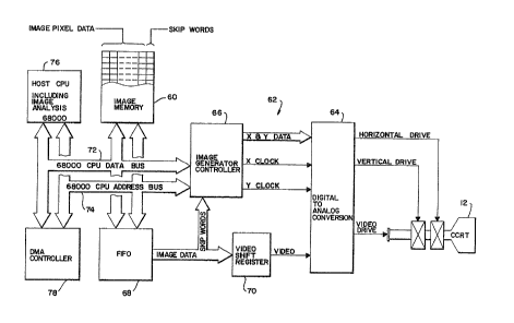
With reference now to FIG~ 2, depicted is
one arrangement of elements in accordance with the
invention, including elements within the electronics
package 48. In FIG. 2, the cathodochromic CRT (CCRT)
of FIG. 1 serves as a display device. An image memory
60 is provided, capable of storing pixel data on a on
line-by-line basis, corresponding to the lines to be
displayed on the CCRT 12. The image memory 60 may
comprise a portion of a larger dynamic random access
memory serving other purposes as well. Other
significant elements in FIG. 2 are an image generator,
generally designated 621 which operates in conjunction
with digital to analog conversion circuitry 64
(including suitable drivers, not shown) for driving
the deflection elements of the CCRT 12. The basic
designs of the image memory 60, the image generator 62
and the digital-to-analog circuitry 64 follow
conventional practice, but with a number of
modifications to enable them to serve the functions
required in the practice of the invention.
4~
~ 15 -
The digital to analog conversion circuitry
64 may be viewed as a digitally addressable linear
defleetion ~enerator, in contrast to Elyback type
deflection conventionally employed in televisions.
The combination of the circuitry 64 with the CCRT 12
permits display lines to be scanned in any order and,
more generally, permits an electron beam for writing
to be directed to any individual pixel.
While other arrangements may be employed, a
particularly advantageous form of image generator 62
is employed herein, which includes an image generator
controller 66, a first in first out ~FIFO) memory 68
and a video shift register 70~ These elements and
their operation are discussed in greater detail
hereinbelow.
From FIG. 2, it will be seen that the system
embodying the invention is microprocessor-based, and
includes a conventional bus structure for
communication among the various elements. In
particular, there is a data bus 72 and an address bus
74, which ~ay also include a control bus, not
specifically shown. Connected to and generally
controlling the buses 72 and 74 is a suitable
microprocessor 76, such as a Motorola Type No.
25 MC68000. To facili~ate data flow, a DMA controller 78
is included, which permits high speed d~ta transfers
among the various elements, without tying up CPU time.
An Hitachi Type No. HD68450 DMA controller is ~j
suitable.
An important subsidiary processor is the
image generator controller 66, which controls the
overall operation of the image generator 62. In
general, the image generator 62 is a high speed
dedicated sub-system that generates signals to deflect
the electron beam along the X- and Y-axis, while
modulating the electron beam to produce an image. The
image is stored in the image memory 60 which, in the
. . , . ~ .
'
': ' :
:
- 16 -
illustrated embodiment, is a portion of general system
memory which the image generator 62 has priority high
speed access to. In the preferred embodiments, the
various functions are, however, somewhat distributed.
For example, the main CPU 76 serves an analysis
function and accordingly writes data to the image
memory 60, and the DMA controller 78 aids
significantly in transferring data at high speed from
the imase memory 60 to the image generator 62.
An importar1t aspect of the invention is the
organization in the image memory 60 of image and
related data. While based on a conventional raster
system, the organization of the data in the memory 60
differs from conventional.
In common with a conventional raster scan
system, in the disclosed embodiment of the invention
the pixels of a raster scan image are arranged
sequentially in memory beginning, for example, at the
top left corner of the image and continuing line-by-
line. In general, data from the image memory 60 is
read by the image generator 62 in synchrony with the
electron beam scan in the CCRT 12, with the memory
contents determining whether the electron beam is to
be turned on or off as it passes a particular pixel.
As one particular example, for a raster
image of 1024 lines of 1024 pixels each, and an image
memory 60 in which pixel data is stored in 16-bit
words, the total memory re~uirement would be 1024/16
words per line times 1024 lines, resultiny in 65~536
words of memory (assuming one bit per pixel). The top
scan line would be contained in the first 64 words,
the second scan line in the next 64 words, and so on.
A significant departure from convention in
accordance with the present invention is an additional
word added to each scan line in image memory 60,
referred to herein as a "skip word". The "skip word"
contains data placed there by either the image
~Z'~ 2~
- 17 -
~enerator controller 66 or other processor (e.g. CPU
76) prior to image generation. At image generation
time, the lmage generator controller 66 in ef~ect
reads the image memory 60 in synchrony with the
electron beam during each scan line, just as in a
conventional raster system. However, at the end of
the line it reads a skip word and uses that to
calculate a subsequent line to be scanned, and moves
the electron beam accordingly. Thus, during operation
16-bit-wide pixel data words are transferred by the
DMA controller 78 from the image memory 60 to the FIFO
68. The image generator controller 66, by control
lines (not shown), causes pixel data words to be read
from the FIFO into the video shift register 70 to be
clocked out bit by bit. The last memory data word of
each line9 is not pixel data; rather, it is a skip
word. Accordingly, rather than being read into the
video shift register 70, ~he skip words are read from
the FIFO 68 into the image generator controller 66 for
calculation of a subsequent line to be scanned.
An architecture in which the invention may
be implemented is described in greater detail
hereinbelow with reference to FIGS. 7 and 8. However,
important principles of the invention will be apparent
from FIG. 2 in conjunction with the following
discussion with reference to FIGS. 3A, 3B, 3C, 4A, 4B,
5A and 58.
Each of FIGS. 3A, 4A and 5A represents, on a
small scale, image bit map data as i~ would be stored
in the image memory 60 for the particular image, and
will be understood to correspond line-by-line with a
displayed image. FIGS. 3A, 4A and SA each represent a
very small display having 18 lines of 33 pixels per
line. Spaces indicate white pixels (not written) and
asterisks indicate black pixels.
FIGS. 3A and 3B together deplct, for
purposes of comparison, a conventional 1:1 (non-
.. ..
"" " ' ~.
lL~'74L!~PZ~
- 18 -
interlaced) display. The lines Oe YIG. 3A are all
scanned in sequence top to bottom as indicatec7 by the
scan order chart of FIG. 3B. At a 1:1 interlace
ratio, there is one scan field in each frame. The
sequence repeats for as many frames as are required.
With conventional phosphors, an indefinite number of
frames are scanned, as the display image disappears as
soon as scanning stops. With a long persistence
display, as is employed in the practice of the
invention, after a finite number of complete frames
have been scanned, contrast is built up to a maximum,
and scanning can stop.
FIG. 3C is an alternative scan order chart
to be read together with FIG. 3A. FIGS. 3A and 3C
together depict, for purposes of comparison, a
conventional 2:1 interlaced display of the same image.
Starting with line 1, the odd-numbered lines are
scanned in sequence to define the first field. Then,
starting with line 2, ~he even-numbered lines in
sequence are scanned to define the second field. At a
2:1 interlace, there are two fields per full image
frame. As noted above, the sequence repeats for as
many frames as desired.
As noted in the Background of the Invention,
higher interlace factors can be useful in long
persistence display~, including storage displays.
Since the imaqes are static, a detailed high
resolution image can be generated at higher interlace
ratios, providing a low resolution image very quickly
that then becomes more detailed as the subsequent
fields are scanned.
As described above with reference to FIG. 2,
an important aspect in the preferred embodiments of
the invention is the use of "skip words" to indicate a
particular successive line to scan. It will be
appreciated that the skip words can be coded in
p~
-- 19 --
various manners, and that the particular coding
described herein is exemplary only.
FIGS. 4A and 4B together depict a 2:1
interlace example employing skip words. The example
of FIGS~ 4A and 4~ generates the same scan sequence
and image as the example of FIGS. 3A and 3C, but it
does it by employing skip words. In the embodiment
described herein, in order to give the image generator
controller 66 enough time to do a calculation based on
a skip word, each skip word is read one line before it
takes effec~, as will be apparent from the following
example.
Considering the example of FIGS. 4A and 4B,
in order to get the process started, the image
generator 62 is initialized to an interlace ratio 2:1
and accordingly expects to commence with line 1 to do
a field of odd-numbered lines, and then again with
line 2 to do a field of even-numbered lines.
Accordingly, the image generator 62 first reads the
bit map data for line 1 from the image memory 60, and
writes it to line 1 of the CCRT 12 display~ At the
end of line 1, a skip word having a value of 2 is read
and temporarily stored within the image generator 62
and the scan is set to line 3, the next odd-numbered
line. While line 3 is being scanned, the image
generator controller 66 has sufficient processing time
to also add the previously-read skip word value of 2
to the current line number (in this case 3), to arrive
at a result of 5, as the next line to be scanned. The
process thus continues as indicated by the FIG. 4B
scan order chart. After line 17 is scanned, the
process is repeated for the even-numbered lines,
beginning wi~h line 2.
While FIGs. 4A and 4B provide a relatively
trivial example, they illustrate the manner in which
each skip word indicates a particular successive line
to be scanned.
`"' :' ': ~ . -
': : ' , ` ':
:: .,, ,.: . ~ . ,
,2~
- 20 -
As a less trivial example, FIGS. SA and SB
together d~pict the sltuation where the skip word
values also reflect which lines, iE any, stored in the
image memory 60 have no inPormation, and accordingly
can be skipped during the scanninq sequence. As noted
above, in order to give the image generator controller
62 time to act on the skip words while the process is
getting started, the first two lines of each field are
scanned, even if they have no picture information.
The scanning sequence depicted in FIGS. 5A
and 5B again begins with line 1, which is read from
the image memory 60 and written to the screen of the
CCRT 12. The skip word having a value of 4 is read,
and temporarily stored within the image generator 62.
While the skip word having a value of 4 is being
processed, scanning proceeds immediately to line 3.
While line 3 is being scannedr the image generator
controller 62 calculates the line number of the next
line to be scanned by adding the skip word value 4 to
the current line number 3, to arrive at a result of 7.
Thus, the next line scanned in sequence after line 3
is line 7. This process continues through both scan
fields, with the ima~e generator controller 62
determining which lines to scan and which to skip,
based on the values of the skip words.
In these examples, while field 1 starts wi~h
odd and field 2 starts with even lines, the lines in
the field will not necessarily be odd in field 1 and
even in field 2. In a more general case, the fields
may be unbalanced, requiring the processor to level
the number of lines each field or create an extra
field to accommodate excess lines in certain fields
that would take longer than desired to scan, ~hile
taking into account the desirabili~y of some form of
power line synchronization.
As noted above, skip words may be coded in
various alternative manners, without departing from
. . ..
, ;;~ ,"".,:,.
. .
. .
L~S~
- 21 -
the scope oE the invention. In a more general case,
the skip word can contain a signed number directing
the image generator ~ontroller 66 to display a line
above or below the last one displayed. Thus, the skip
word could provide positional data relative to the
last line scanned. A special code could be employed
whereby a line would be scanned twice in the current
field, making it "bolder" on the display. As another
possibility, the skip word could be coded as an
absolute line number, rather than as a relative
offset.
As the image generator 62 is computing the
order of scan lines based on ~he read skip words, the
image generator 62 expects the DMA controller 78 to
transfer lines from the image memory 60 to the FIFO 68
in the same orderO This is accomplished by having the
processor which sets up the skip words in the image
memory 60 at the same time generate a conventional
link map for the DMA controller 78 which corresponds
to this order of lines.
Mentioned but not discussed in detail above
is the mechanism which writes the skip words to the
image memory 60 in accordance with the desired
interlace ratio and in accordance with lines which are
to be skipped. This particular mechanism is herein
termed "analysis means", and represents one of the
functions perEormed by the CPU 76. It will be
appreciated that the functions of the present
invention are distributed among the various elements,
with great flexibility resulting from the fact that
the system is microprooessor-based. Thus, the
analysis means comprises the CPU 76 and suitable
programming therefor, the algorithm for which is
described next below.
Preliminarily, however, it should be noted
that the bit-map image is stored in the image memory
60 in an entirely conventional manner, the image being
,,
..
. ~,
'
~27~.?;Z8
-- 22 --
developec] ~rom any suitable external source.
Initially, the skip words are not set~
An initial step in the routine of the
analysis means is to determine which lines, if any,
S have no picture information~ Assuming a binary "0"
indicates a particular pixel is off, and a binary "1"
indicates a particular pixel i5 on, the determination
of which lines contain no picture information is a
relatively trivial one, and involves simply examining
the pixel data for each line~ If at least one "1" is
found, then that line does contain pixel information.
If the line is all "O's", then that line contains no
- picture information.
The next step in the routine of the analysis
means is to choose an interlace ratio. The alogrithm
attempts, if possible, to select the lowest interlace
ratio which will achieve a field rate in the order of
30 Hz. However, the interlace ratio will normally not
be permitted to be less than 2:1, in order to avoid
the effects of heat conduction between adjacent lines.
Specifically, the number of lines to be
scanned is determined by taking the total number of
lines in the display (for example 2048), and then
subtracting the number of lines determined to have no
picture information.
The number of lines to be scanned is
multiplied by the scan time per line which, for
example, is ~80 microseconds. This gives the time
required for a complete frame, neglecting, for
purposes of simplified example, the time required for
vertical retrace. The frame period is then divided by
1/30 seconds, which is the period for a single field.
The result, after rounding up to an integer number, is
the interlace ratio.
Again, the above example is simplified,
because time must also be allowed for the vertical
~ ~7 L~ 3
- 23 -
retrace interval, including calculations which may be
necessary during the vertical retrace interval.
If the interlace ratio becomes unacceptably
high, then the field rate can be reduced to 15 Hz. In
order to avoid the effect of any stray 60 Hz AC fields
which may enter the system, it is desirable to make
the field rate a sub-multiple of 60 Hz, e.g~ 30 Hz or
15 H2.
While a calculation approach is described
just above for determining the interlace ratio, pre-
determined calculation results can be stored in a
look up table or similar software technique in order
to minimize the time required for calculation.
With the lines to be skipped and the
interlace ratio thus determined, the CPU 76 then
establishes the skip words in straightforward manner
to direct the scanning sequence of the image generator
62 to achieve the desired interlace while skipping
blank linesO At the same time, ~he link map for the
DMA controller 78 is correspondingly established.
So that the image generator controller 66
can properly initiate the process of reading lines
from the image memory G0, the thus determined
interlace factor is also directly communicated to the
image generator controller 66.
Detailed Description -- Rolling Writinq
~ he discussion up to this point has assumed
that the image memory 60 includes pixel data for an
entire image before any writing commences. There are
two situations addressed by the invention where such
is not the case, and specialized techniques are
employed~
The first of these situations occurs when
only a partial raster-scanned image is available, such
as where an image is being received line-by-line in
real time from a facsimile transmission over a
telephone line, for example, or from a local document
. : -. .. : : ,
.: ' .,..,- . ~ : - - '
~,
}~
- 2~ -
scanner or digitizing camera~ In qeneral, A eacs imile
image takes approximately 35 to 40 seconds to arrive.
Under these conditions, pixel data is placed line by
line into the image memory 60 as it is received. A
window of, perhaps, 128 lines is rolled down the image
memory 60 bit map. This causes the image to appear
gradually Erom the top down, while building contrast.
Due to the overheating considerations discussed in the
"Background of the Invention", a single line cannot
simply be colored to contrast before moving to the
next.
More particularly, a window size is defined
comprisingr for example, sixteen blocks of eight lines
each, for a total of 128 lines in the window. Thus, a
window means, embodied in the host CPU 76, selects a
subset of image lines in the image memory 60.
Once the image memory 60 has received a
sufficient number of lines to generate a window, the
image generator 62 begins making repeated scans
reading the image pixel data from the image memory 60
and writing to the CCRT 1~ When eight additional
image lines have been received, enough for a new
block, the scanning window is in effect rolled down,
picking up the new block, and dropping off the oldest
block. In other words, the window means adds lines to
the subset of lines comprising the window in units of
a block, and deletes old lines from the subset in
units of a blcok. This procedure continues until the
entire imaqe has been received. Programmable
interlace and skip could be employed in the scanning
of the rolling windows, but the processor time
required to continually recalculate interlace,
configure skips, and build a link map for the DMA
controller 78 is excessive.
In most cases, image data arrives from a
scanner or similar device and is placed in the image
memory 60 at a rate which does not permit writing the
: : ,
,
- ~s -
CCRT 12 to full contrast, if the system is to present
new lines as they are received in essentially real
~ime. Accordingly, after the entire scanned image has
been received, the entire image is analyzed and skip
words generated as described above, and the system
reverts to the previously-described operation to bring
the display up to full contrast.
Another situation where it is desired to
display incoming data as it is received in as close to
real time as practicable is in the case of manual
annotation of an image which is currently being
displayed. Annotation is implemented employing a
direct point writing technique wherein a line on the
screen follows a continuous stream of X, Y pixel
addresses from an external source such as a graphic
digitizer tablet (not shown). A person handwrites on
the digitizer tablet and a line appears~ apparently
simultaneously, on the display. In general, this is
accomplished by taking point position information from
the graphics tablet in a stream of X, Y positions,
translating them into X, Y pixel addresses on the CCRT
display, and darkening the address pixels with the
electron beam in real time.
This input mode causes the same exposure and
heat problems discussed earlier. In general, new
points arrive too quickly for each pixel to be written
to full contrast. A variation on the rolling writing
approach is employed, implemented as a point refresh
memory depicted in FIG. 6 and preferably included in
the image generator controller RAM 86 (FIG. 7, below).
Depending upon the speed upon which input
points are arriving it is not always possible to
achieve full contrast. A somewhat arbitrary
compromise is adopted wherein 1 millisecond per point
is allotted to achieve the best contrast possible in
this limited amount of time. In general, this allows
approximately 6 to 8 exposures per point. In order to
~` ~
.,
~'7~ 2
- 26 --
make the line more visihle on ~he screen, the electron
beam is deEocused for a wider trace, with a
commensurate increase in beam ener~y.
FIG. 6 represents an organi2ation of data in
memory herein termed a point refresh buffer,
maintained by the image generator 62. As indicated in
FIG. 6, a rolling window for annotation contains a
number of pixel points, rather than a number of scan
lines. In order to keep the hardware requirements
reasonable, the technique as implemented employs a
relatively small window, of eight points, (an
arbitrary figure which may be varied). Each point in
the window is represented by a block of memory
locations respectively containing the X pixel
position, the ~ pixel position, and a refresh counter
location in which a eount of the number of times each
particular pixel has been written is maintained. In
order to ensure that a particular pixel is not
overexposed, and thus erased, a delay factor is also
included. If there are a number of points, then the
delay factor applies from one point to the next. In
the limiting case where there is only one point to be
displayed, the delay factor is applied to control
successive exposures of that one point. The point
refresh buffer could be expandecl to include other
in~ormation, such as video drive data, focus values,
settling time from previous points and so on.
The algorithm for point writing will now be
considered.
1. First, the image generator 62 positions
the electon beam in the CCRT 12 to the pixel address
of Point 1.
2. N~xt, a delay is introduced, to
accommodate deflection settling time, plus the Point 1
delay factor time.
3. Next, the electron beam is turned ON
then OFF for a predetermined time duration.
. .
- 27 -
4. The reÇresh count for Point 1 is
decremented.
5. In the event the Point 1 refresh counter
is zero, then data for a new Point 1 is obtained and
placed into point refresh the buffer, if such data is
available.
6. The image generator Ç2 then checks the
point refresh buffer for Point 2. If the Point 2
refresh counter is zero, then Point 2 is skipped.
Otherwise~ the electron beam is positioned to display
Point 2, which is displayed as summarized above.
As data for new points arrives, their
display addresses are calculated and are held in a
separate first-in-first-out memory bufer maintained
by the CPU 76, and are passed on demand to the image
qenerator 62 to be placed in the point refresh buffer.
The image generator 62 rolls through the point refresh
buffer and colors each point the prescribed number of
times to build its contrast.
If, as an example, a line is being drawn
left-to-right across the screen, at any given time
eight points along the line will be in the point
refresh bufferO The left-most point being the first
received, will finish its refresh first, and be
replaced by the next point along the line, and so on,
making a tiny window rolling along the line following
the pen. In practice, the procedure occurs too fast
for the human eye, so contrast differences are not
discernable at the leadinq edge of the line as it is
being drawn.
Detailed Description -- Hardware Details
With reference now to FIGS~ 6 and 8, a
suitable hardware implementation of the system of FIG.
2 is shown in greater detail. FIGS. 7 and 8 herein
correspond to FIGS. 3 and 4 of the above-incorporated
related application Serial No. 789,107, to which
reference may be had for further details of FIGS~ 7
~D
~7~
- 28 -
and ~ with wh.ich the present invention .is not direc-tly
concerned.
The d:igital-to-analog conversion circuitry 64 of
FIG. 2 generally corresponds to FIG. 8, which depicts in
detail circuitry termed herein an "analog front end" 72.
The image generator 62 communicates with the analog front
end 72 by way of an "Image Generator Internal" (IGI) bus.
The IGI bus is a simplified control bus for causing the
loading of various registers in the analog front and
circuitry 72 with digital values at appropriate times.
The IGI bus is driven by bus driving logic 74 which
includes conventional elements such as latches and
buffers, and could be implemented, for example, employing
conventional parallel input/output (PI0~ compatible with
the image generator controller processor 66.
As noted above with reference to FIG. 2, the
image memory 60 preferably is a portion of general system
memory, shown in FIG. 6 as dynamic RAM 78 connected to
the host CPU data and address busses 72 and 74.
Also on the busses 72 and 74, and depicted in
generalized form, is a port 80 Eor "other I/0" which
represents interlaced external systems, such as systems
for defining an image to be displayed.
Two other elements on the busses 72 and 74,
with which the present invention is not directly
concerned, are a "per~onality memory" 82 and sample
circuitry 84. These elements are described in much
greater detail in th~ above-mentioned related application
Serial No. 520,790.
Considering the image generator 62 in greater
detail, the image generator controller 66 is preferably a
special high speed processor dedicated to operating the
display and performing its functions with a minimum of
involvement by the host CPU 76. It should be noted that
the designs of the FIG. 7 image
"
~'` `
.
- 29 -
generator 62 and the FIG. 8 analog front end 72 are
interdependent and may be altered considerably,
particularly at the interface between the two
subsy~tems .
To implement the imaye generator controller
66, a Zilog Type No. 8594 "Universal Peripheral
Controller" is employed. The 8594 is a specialized
processor which appears to the 68000 host CPU 76 as
twenty registers in the 68000 address space.
Connected to the 8594 controller 66 is a RAM
86 in which program and data are stored during
operation. Upon system reset, it is a characteristic
of the 8594 that it expects data (including program
da~a) to be uploaded via selected ones of i~s twenty
registers into the RAM 86. Thus, as a part of the
system initialization procedure, the host CPU 76
uploads this data from the EEPROM memory 82 into the
RAM 86.
To provide ON/OFF video at a pixel clock
rate of 10 MHz, corresponding to a period of 100
nanoseconds, the sixteen bit-wide first-in-first-out
(FIFO) memory 68 is connected to the address and data
busses 72 and 74 to receiver image data, and a
serializer 68 is connected to the output of the FIFO
68. Operation of the FIFO 68 and serializer 72 is
coordinated by a high speed state machine 88,
implemented in a programmable logic array ~PLA), which
simply acts as a high speed clock and timing
generator, under the overall control of the controller
66. The controller 66 has a connection ~not shown) to
the DMA controller 78 to cause image data to be
transferred at high speed from the bit-mapped image
memory 60 to the FIFO 68 until the FIFO 68 is full.
This architecture permits the use of a slower but
wider RAM for the bit map 60 which can be read at
conventional speeds since multiple pixels are read at
X~,~
- ~30 ~
one time, while at the same time accommodating
relatively high speed pixel output.
During electron beam erase operation image
c3ata is not relevant, and the input to the serializer
70 is forced to a logic "1".
With reference now to FIG. 8, the analog
front end 72 generally comprises a digital to analog
interface section 200 and a polynomial expansion
function generator section ~02 which accepts X and Y
digital position coordinate data~ and applies
appropriate geometry correction ~o generate drive
signals for the focus and deflection elements of the
CRT 12. In general, the analog front end 72 may be
described as an integrated digital to analog control
board which drives the cathodochromic CRT display tube
12. The analog front end 72 provides functions such
as electron beam positioning, focusing and control of
video drive levels.
An important hardware device, a number of
which are employed in the analog front end 72, is a
multiplying digital to analog converter (MDAC), A
suitable MDAC is an Analog Devices Type No. AD7524,
which includes an 8-bit data register. Each MDAC has
an analog input and an analog output. The output
voltage (assuming current-to~voltage conversion as
required) is equal to the input voltage multiplied by
an attenuation factor determined by the value stored
in the 8-~it register. The MDAC registers are
connected to the IGI bus, and individually addressed
via suitable address decoding circuitry ~not shown).
In the symbology of FIG. 8, each MDAC is represented
by a box having a term in parenthesis, which
represents the coefficient value stored in the
register, as communicated through the IGI bus in a
conventional manner. Several of the ~.DACs are used to
provide offsets and have an analog input represented
as "1.0', which designates simply a fixed reference
.
':;; ..
: :
~2~
- 31 -
voltage such that th~ output of the particular MDAC
clirectly represents the register value times the
reference voltage.
Considering the digital-to-analog interface
section 200 in greater detail, for receiving the
diqital position data, an X-counter/latch 204 and a Y-
counter/latch 206 are provided and appropriately
connected to the IGI bus. Conveniently, each of the
counter/latches 108 and 110 comprises an 11-bit
counter whi~h can be configured to count in an up or
down mode. Considering the X-channel, for example,
this allows the display to be conveniently scanned
from left to right or right to left.
Immediately following the X-counter latch
204 is a digital-to-analog converter 208 for the X
channel, and a similar digital-to-analog converter 210
for the Y channel follows ~he Y counter 210. The
output of the X DAC 208 is an analog representation of
a desired X-axis position, and is applied to various
points within the polynomial expansion function
generator section 202 as indicated. Althouqh not
specifically shown, it will be appreciated that level
converters are included where required, depending upon
the particular components selected.
The output of ~ DAC 210 is similiarly an
analog representation of a desired Y-axis position.
For proper compensation, an offset Y-axis
representation, Y', is required, as well as inverted
offset Y-axis representation, Y'. To generate these,
an analog summation element 212 is provided having its
inputs connected ~o the Y signal and to the output of
an MDAC 214 outputting a representation of a value
INITIAL Y OFFSET/ and having its output connected to
an inverter 216.
Also connected to the IGI bus is a 12-bit
digital-to-analog converter ~DAC) 218 for providing a
STATIC FOCUS signal. An internal register (not shown)
..
'
~ ~,'7~
- 32 -
wlthin the static focus DAC 218 is loaded with a
constant value for the particular mode oF operation.
Di~ferent focus ~alues are employed Eor writing and
erasure. The output of the DAC 218 is connected
through a suitable line driver (not shown) and then
through the FIG. 2 a power amplifier (not shown) to
drive appropriate control elements of the CRT 12,
specifically, the static focus coil 44.
~ video amplifier 200 is included, the
output of which is connected in a conventional manner
to the cathode and control grid of the CRT 12. In the
system depicted, no gray scan is employed, and
individual pixels are either OFF or ON. The drive
level for an ON pixel, and also drive level for
electron beam erase, is established by a signal level
applied to an analog input 222 of the video amplifier
220. This input is supplied by another 12-bit DAC
214, comparable to the DAC 218. To complete the video
drive circuitry, the ON/OFF video drive line from the
FIG. 3 serializer 110 is connec~ed to a BLANK/UNBLANK
input 226 of the video amplifier.
It will be appreciated that this video
circuitry is exemplary only. For example, multi-level
(gray scale) video can be provided by combining the
outputs of a relatively fast DAC for modulation and a
relatively slower but larger DAC for establishing a
base level.
The function generator section 202 of FIG. 8
in general qenerates geometry correction polynomials
which dynamically vary as a function of X and Y screen
positions. These are described in greater detailing
the above-incorporated related application Serial No.
789,107, and are only briefly summarized herein.
More particularly, the geometry correction
polynomial for the X channel is as follows:
XDEFL = D ~X ~ AX3 + BXY' + CXY'2 + XOFFSET)
-
: '. ' '' ' ,
..
. . ,~ -: . - .
-~:,. , . ~:
.11.d~d ~ J_3
-- 33 --
The coefficients A, B, C, D and XOFFSET are
employed as constants, while X and Y' are screen
position data.
The above-polynomial for XDEFL is generated
by the elements within a function generator 228.
The geometry correction polynomial for the Y
channel is similar, and is as follows:
YDFFL = H (Y' + EY'3 ~ IFYI~ + GY'X2 +
OFFSET)
Again, the coefficients E, F, G, F3 and
YOFFSET are employed constants.
The above polynomial for YDEFL is generated
by elements within a f~nction generator 230.
Following the function generators 228 and
230 are suitable drivers and power amplifiers ~no~
shown) connected to control elements of the CCRT 1~.
For dynamic focus, a polynomial function
generator 232 generates the function:
DF DEFL = I (X' ,2 f y~ .2 + DFOFFSET)
where X'' = X + DF XOFFSET and
Y'' = Y + DF YOFFSET
The manner in which the image generator 62
of FIG. 7 and the analog front end 72 of FIG. 8
operate together to drive the display will now be
considered. To begin a scan line, the CPU 66 sets the
X- and Y-counter/latch registers 204 and 206, and then
triggers a cycle of the high speed state machine 88,
which cycles at a rate of 10 MHz through n sets of 16
states each to generate appropriate timing signals for
a scan line containinq n x 16 pixels. Included in the
-
control lines is an XCLOCK signal, which clocks the X
COUNTER/LATCH 204 to drive the electron beam
horizontally at a constant rate. At the same time,
data is clocked from the shift register 70 into the
video amp 220, the shift register 70 having been
loaded from the FIFO 6B~ The shift register 70 can
hold 16 bits at a time. To reload the shift register
.
,~ .
'
:;
1~ 7 ~P,~
- 3~ -
70 so that video can continue uninterrupted, at the
13th clo~k pulse, a FIFO 68 read cycle i5 initiated.
The FIFO 68 comprises Moskek rrype No. MK4501 devices,
and the shift regis~er 70 comprises conventional
digital video shift registers which are intended to
operate together in this matter.
While the shift register 70 is reading data
from the FIFO 68, the DMA controller 78 reads 16-bit
words from the bit-mapped image RAM 60 and loads these
words into the FIFO 68.
At the conclusion of a scan line, the image
generator controller 66 sends a "count done" signal,
and the serializer 70 completes its current cycle. At
this point, a "skip word" is available to the image
generator controller 66, which is ~hen employed to
determine a subsequent line to be scanned.
While specific embodiments of the invention
have been illustrated and described herein, it is
realized that numerous modifications and changes will
2n occur to those skilled in the art. It is therefore to
be understood that the appended claims are intended to
cover all such modifications and changes as fall
within the true spirit and scope of the invention.
,:
. .
'' ;,' ' ~ ,
. .
: