Note: Descriptions are shown in the official language in which they were submitted.
7~
-- 1 --
The present invention relates to a circult
for producing a clock signal for reproducing a PCM (pulse-
code modulation) signal for use in record reproduction
~ systems, such as VTRs or digital audio tape recorders of
; ~ 5 the rotary head type (R-DAT).
~ A PCM signal is reproduced using a clock
- signal (fch=9.408 MHz) having twice the frequency of the
minimum bit:pulses of the PCM signal (hereinafter referred
to as "PCM signal frequency").
iO ~ A PCM signal is recorded, for example, on a
magnetic tape, which is thereafter helically scanned by a
magnetlc head mounted on a cylinder rotating at a high
speed for reproducing the signal in various modes, for
: example, high-speed search, normal mode or trick reproduc-
tion, or for monitoring during fast forwarding or rewind-
ing. A PLL (phase locked loop) circuit is used for read-
ing the reproduced PCM signal.
!;
j,i~ i
Conventional PLL circuits comprise a phase
comparator, low-pass filter, limiter circuit and
voltage-controlled oscillator (VCO).
When the speed of a magnetic head relative
to an associated magnetic tape is difEerent fro~ that
in a normal reproduction mode, the PCM signal from
the head has a different frequency. Accordingly, the
circuit is adapted to automatically vary the reproduc-
tion clock frequency fch (i.e. channel clock frequency)
in accordance with the difference. The reproduced PCM
signal from the head and the reproduction clock signal
from the VCO are negatively fed back to the phase com
parator.
In conventional PL~ circuits, the operating
range of the VCO is restricted to the neighborhood of
the desired frequency by the limiter circuit so that
the reproduction clock is not locked at an improper
- frequency. However, if the reproduced PCM signal fre-
quency varies beyond a limit, a reproduction clock sig-
nal having a frequency outside the operating range of
the VCO is needed. The conventional circuit therefore
has the problem of being unable to reproduce the PCM
signal data in such cases.
~7~
~nexami.ned Japanese Patent Publication SHO
62-8354 and "Radio Technology," April 1987, pp. 7~-77
discloses a method for use in a special reproduction
mode wherein -the speed of rotation of the head cylinder
is altered to use a reproduction clock signal of normal
frequency. Nevertheless, this method involves the
problem that the rotational speed of the cylinder motor
must be controlled to maintain the head cylinder at a
definite speed relative to the magnetic tape.
An object of the present invention is to
provide a circuit which produces a clock signal by auto-
matically shifting the frequency band of the reproduc-
tion clock signal produced by a VCO by a suitable amount
when the detection head reproduces a PCM signal in
normal and special modes, to obtain a suitable reproduc-
tion clock signal in accordance with variations in the
PCM signal frequency.
. A VCO control signal may be produced by detect-
ing the tape speed Vt and the head speed Vh and then calcu-
lating by means of a detection circuit.
A VCO control signal may be prepared from a
single-freque~cy signal recorded ln the front or in
the rear of the PCM signal record area on the signal
record track of the recording medium, by converting
the variation ln the frequency of the signal to a
voltage signal by means of a frequency/voltage converter.
i~
~7~
-- 4 --
A circuit which is operably free of errors
even when the characteristics of the frequency/voltage
converter are not in register with the voltage-frequency
characteristics of VCO may be provided.
Fig. 1 is a block diagram showing an embodiment
of the invention;
Figs. 2 and 3 are block diz_-ams showing other
embodiments of the invention;
Fig. 4 is a diagram illustrating the operation
of a VCO included in the embodiment of Fig. 1;
Fig. 5 is a diagram illustrating tne operation
of a VCO included in the embodiment o Fig. 2;
Fig. 6 lS a vector ciagram showing a variation
in the frequency of a PCM signal;
lS Fig. 7 is a diaqram illust-a-ing a signal
record area formed in the recording t ack on a magnetic
ta~e;
Figs. 8a to 8f are signal dlagrams of a
channel clock frequency detection circuit included in
the embodiment of Fig. 3;
.J,
? '~
Fig. 9 is a diagram showing the difference
between F-V convierter and VCO in input-output character-
istics;
Figs. 10 and 11 are block diagrams showing
other embodiments;
Fig. 12 is a diagram showing a conventional
PLL circuit; and
Fig. 13 is a diagram showing the operation of
a VCO included in the circuit.
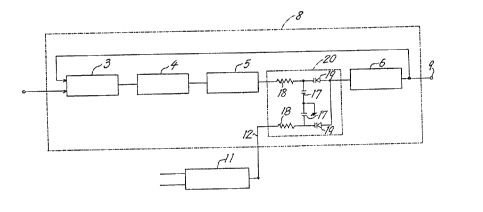
Fig. 1 shows a PLL circuit 8 for a PCM signal
el~bodying the invention.
A cylinder motor 7 rotates a head 1, which
reproduces the PCM signal recorded on a magnetic tape 2.
The reproduced PCM signal obtained from the head is fed
to a phase comparator 3 included in the PLL circuit 8. A
control signal having upper and lower limits is fed to an
adder 10, from a low-pass filter 4 and a limiter circuit
5, to a VC06. The VCO 6 produces a clock signal for re-
producing the PCM signal, feeds its output to a terminal
9 and, feeds back its output to the phase comparator 3.
A band control signal 12 from a channel clock
frequency detection circuit 11 is also fed to the adder
j, .,
~7~4
-- 6 --
i
10 at the same time as the control signaL
The output from the adder is fed to the voltage-controlled
oscillator, (VC0), 6. The control sic~nal 12 sets the
output frequency band of the VC0 6.
The channel clock frequency detection circuit
11 detects the variation ratio of thle frequency f of
the PCM signal reproduced by the head to the PCM signal
frequency fO for normal reproduction and produces the
band control signal 12 which is in proportion to ff~.
With reference to Fig. 6, ~ is the inclination
angle of the track when the tape is at rest and is 622'
in the case of a digital audio tape recorder of the
rotary head ~ype. ~ is the inclination angle of the
track during the travel of the tape a.~d is 622'59.5".
lS Vt' is a component, in the lengthwise direction of the
tape, of the vector of the speed of the head relative
; to the tape during high-speed reproduction. Vh' is the
- vector of rotational speed of the head during high-speed
reproduction. v' is the vec~or of act~al spe2d of the
head relative to the tape during high-speed reproduction.
With reference to the vector diagram, V' = Vh' + Vt'.
Vt is a component (8.15 mm/sec), in the length-
wise direction of the tape, of the vector of the speed
of the head relative to the tape during normal reproduction.
Vh is the vector (3.14 m/sec) of rotational speed of the
~, head during normal reproduction.
.j . ,
_ 7 _
Since ~ component V0' of Y' in the direction of
the tr~ck is proportional to the recluency of the
reproduc~d PCM signal,
~ V0' = Vh'cos(~ - 90) - Vt' cos ~.
S During no~l reproduction,
fO ~ V0 = Vh cos (~ - ~0) - Vtcos a~
so that
f/fO = V0'/V0
Vh' cos (~ - ~0) ~ Vt'cos~ (1)
Vh cos (~ - ~0) - Vtcos ~
The head speed Vh or Vh' is obtained.by feeding
to a head speed detection circuit 26 2 signal from a
pulse generator PG disposed close to tne rotary shaft of
the cylinder motor 7. The speed of tra~el of the tape,
Vt or Vt', is obtained by feeding a rotation signal from
a capstan motor or reel motor 24 to a tape speed detection
circuit 25.
~ he channel clock detection circuit 11 feeds to
the adder 10 the band control signal 12 in proportion to
the ratio f~fO calculated from the eq~ation (1). For
no ~ 1 reproduction, the central freq~ency of the reproduc-
tion signal to be produced by the VC0 6 is adjusted in
the central hatched range 14 shown in Fig. 4 and limited
by the limiter circuit 5. When the ro~ational speed f
the cylinder remains at the same leve} as in the normal
~79~
reproduction mode, the centr~l frequency of the reproduction
clock signal shifts to a region lS for reverse-dixection
special reproduction, or to a region 1~ for forward-
direction special reproduction. Thus, the regions 14,
lS and 16 include channel clock frequencies of reproduction
clock pulses in conformity with variations in the PCM
signal in the respective signal reproc~ction modes.
Fig. 2 shows another embodiment of PLL circuit
B, wherein the adder 10 of the first e.~bodiment is
replaced by a variable capacitance circuit 20 comprising
capacitors 17, resistors 18 and a var_2ble capacitance
diode 19.
An output band control signa: 12 produced by
a channel clock frequency detection circuit 11 using the
same arrangement as in the embodiment of Fig. 1 gives the
; VCO 6 the input-output characteristlcs 21 or ~ormal
reproduction, 23 for forward-direction special reproduc-
tion or 23 for reverse-direction special reproduction
as seen in Fig. 5.
Fig. 3 shows another embodiment of channel
clock frequency de~ection circuit 11, ~-hich utilizes
a signal of single frequency (~ fch or 16 fch, where
fch = 9.408 MHz? recorded at a specifi~d position in a signal
track format on the magnetic tape. For high-speed search
operation, the single-frequency signalin the specified position
y~
~7~fl
is extracted to produce a signal in accordance with the
channel clock frequency of the reproduced PCM signal.
With reference to Fig. 7, a track 13 on
the magnetic tape 2 has a PCM signal recording area 60,
interblock margin areas 61 at front and rear of the
area 60, and margin areas 62 at the starting and terminal
ends of the track. A signal of single frequency 1 fch or
6 fch is recorded in the margin areas 61, 62 to ensure
erasure of the previously recorded signal when another
signal is superposed on the tape.
The single-frequency signal recorded in one
of the margin areas 61, 62 is extracted to produce a VCO
control signal 12 in accordance with variations in the
frequency of the reproduced single~frequency signal.
A timing signal e indicating the passage of -
the head over the margin area 61 or 62 on the track 13
~ is produced by a first gate circuit 30 which receives
- an RF change-over signal a from a terminal 34. The
signal e produced is a gate signal indicating the repro-
duction position of the single-frequency signal on a time
axis.
During high-speed reproduction, the head
passes across tracks, so that the RF signal from the head
includes a signal reproduced from tracks with the same
azimuth angle as the head and a signal reproduced
from tracks wi-th a reverse azimu-th angle to the head,
which appear alternately. However, since the signal
reproduced from the tracks of reverse azimuth angle is
not usable, a second gate circui-t 35 removes this signal,
extracting the other signal only from the tracks of the
same azimuth angle to form a gate signal d.
Figs. 8a to 8f show the forms of signals at
various portions. When an RF signal _ is fed to an AM
detection circuit 27, this circuit produces an output _
having alternating crests and furrows. When the head
is on the tracks of same azimuth angle, the RF signal
exhibits an increased amplitude to form crests of the
output c, whereas when the head is on the tracks of
reverse azimuth angle, the amplitude of the RF signal
diminishes to form furrows of the output c.
The output c is compared with an output vo
from a suitable reference voltage source 28 in a
voltage comparator circuit 29, whereby the signal portion
below the potential level vo indicated in a dot-and-dash
line in Fig~ 8c is eliminated to give an on~track output
d. Thus, the portion where the output e from the
first gate circuit 30 overlaps the output d from -the
compara-tor circuit 29 is an effective reglon of single
frequency, and a gate signal f representing this position
~5 is produced by an AND gate 31.
--10--
On the other hand, -the RF signal b reproduced
by the head 1 is also ed to a frequency/voltage
converter circuit (F-V circuit) 32, which produces an
output with a potential in proportion to the frequency
of the RF signal, and this output is clelivered to a
sample holding circuit 33. Accordingly, by sampling the
single-frequency signal at the positions represented by
the gate signal f, a control signal 12 is available
which represents the variation in the frequency of the
reproduced RF signal, i.e. in the channel clock frequency
of the PCM signal. The signal 12 is held in a capacitor
45 and also fed to an adder circuit 10 in the PLL circuit,
whereby the frequency of the reproductlon clock signal
to be produced by the VCC can be varied in conformity with
the contemplated PCM signal reproduction mode. The
operating range of the VCO 6 can therefore be shifted
toward the forward-direction reproduction mode or
reverse-direction reproduction mode.
The present invention can be embodied not only
for VTRs and R-DATs but also other reproduction systems
such as disc reproduction systems, i.e. for reproduction
5ystems ~or use with recording media having recorded thereon
j at least a PCM signal and a single-frequency signal on a
time division basis.
~L27~
Furthermore, a plurality of heads can be
arranged on the pa-th of travel of -the tape for reproducing
the PC-~ signal and -the single-frequency signal at different
positions at the same time.
With the embodiment of Fig. 3, variations in the
frequency of the single-frequency signal are converted
to variations in voltage, which are fed to the VCO 6 to
alter the operating range of PLL; so that the F-V converter
32 must be in agreement with the VCO 6 in input-output
characteristics. This will be described with reference
to Fig. 9. Since the frequency fc of the single-frequency
signal to be detected has the relation of fc = 1/2 fch,
the input-output characterlstics of the F-V converter,
as doubled in input frequency fc and plotted as ordinate,
can be compared with the input-output characteristics of
the VCO 6 as seen in Fig. 9. With reference to Fig. 9,
F-V curve and VCO curve have the same value at an input
fl of the F-V converter. Accordingly, the central
frequency of the VCO 6 is in conformity with the PCM
signal frequency.
However, F-V curve and VCO curve are different
in inclination in the vicinity of the right and left
ends of Fig. 9, so that when a signal of frequenc~ E2 is
applied to the F-V converter 32, the converter produces
a voltage of V2, which is fed to the VCO 6, with the
-12-
result tha-t the reproduction clock pulses delivered
from the VCO 6 have a central frequency of f2' involving
an error of ~f2. Further when a signal of frequency f3
is fed to the F-V converter, the VCO is set to a central
frequency of f3' involving a greater error (~f3) due to
the nonlinear VCO characteristics. Thus, there arises
the proble~ that the desired central frequency is not
settable owing to varying degrees of inclination and
nonlinearity of the VCO characteristics.
In the case of the embodiment of Fig. 10, the
central frequency of the reproduction clock pulses
produced by a PLL circuit 8 is compared with the frequency
fc of the single-frequency signal detected by the head,
and the difference voltage is fed bac~ to the PLL circuit,
whereby an accurate central frequency is settable
irrespective of the inclination and nonlinearity of the
input-output characteristics of the VCO 6 included in
the PLL circuit 8 to overcome the above problem. The
PLL circuit has an adder 10, to which an electronic
switch 37 is connected at one of its input terminals. A
:
capacitor 45 for holding a central frequency control
voltage is connected to the other input terminal of the
adder. Electronic switches 37 and 44 are controlled by
the output signal f of the gate circuit 43 described
with reference to the embodiment of Fig. 3, such that
-13-
~27~
when the gate signal f indicating the position of the
single-frequency signal is produced during the period
of one revolution of the head, the switches 37, 44 are
closed at H side. Consequently, the adder 10 is
connected at one input terminal to a constant-voltage
generator 38 and at the other input terminal to the
holding capacitor 45. During the remaining portion of
the period, the electronic switch 37 is closed at L
side, connecting the adder to the low-pass filter 4
and forming the closed loop of the PLL circuit. The
circuit then produces data reproduction clock pulses
synchronized with the PCM signal in phase. With the
electronic switch 37 closed a-t H side, a constant
voltage is applied from the generator 38 to the above-
mentioned one input terminal of the adder 10 to controlthe central frequency of the VCO 6.
The single frequency fc to be detected is
further fed to F-C converter B 39 and thereby converted
to a corresponding voltage. With the present embodiment,
the frequency fc to be detected and the data reproduc-tion
clock frequency fch have the relation of:
fc = l/2.fch,
so that the output of the VCO 6 is passed through a
1/2 divider 40 and then converted to a voltage by F-V con-
verter A 41 having the same input-output characteristics
-14-
~4
as -the F-V converter s 39.. The converter A 41, when
made different from the converter B 39 in characteristics,
eliminates the need to use the divider 40. The output
vol.tage difference between the F-V converters A, B is
amplified by an error amplifier 42. In the control mode
wherein the sample holding switch 44 is closed by the
gate circuit 43, the error voltage is applied to the
VCo control voltage to give a central frequency fch of
2 fc by negative feedback. When the gate circuit 43
opens the switch 44, the error voltage is held in the
holding capacitor 45 to fix the central frequency.
Through the operation described above, the
central frequency is adjusted to fch, for exa~ple, once
during one-half revolution of the head in the case of
R-DAT, and a pCM signal reproduction clock signal is
produced without the restriction by the characteristics
of the VCO 6.
The mode signal generator 43 can be any circuit
in addition to those.included in the foregoing embodiments
insofar as the single-frequency area is detectable.
Fig. 11 shows another embodiment of the inven-
tion in connection with the embodiment of Fig. 10.
This embodiment additionally has a capacitor 46 for
holding an F-V converted single-frequency signal from
the F-V converter circuit 32, and electronic switches 47,
--15--
~2~
43 operable by the gate signal f from the gate circuit
43 for changing over the input and output of the F-V
converter circuit 32 to H side.
3uring the cycle of one revolution of the head,
the gate clrcuit 43 produces a second gate signal pulse _
with a slight time delay from the gate signal ~
corresponding to the single frequency area, and the second
gate signal pulse _ operates the switches 37 and 44.
During one cycle period of one revolution of
the head, the F-V converter circuit 32 has its input
and output changed over to L side or H side once or
a plurality of times by the switches 47, 48. When these
switches are closed at H side, the RF signal is fed
to the F-V converter circuit 32, which produces a voltage
according to the single-frequency signal for a capacitor
46 to hold the voltage. During the period other than
when the gate signal f is produced, the swltches 47, 48
are closed at L side, and the negatively fed-back
reproduction gate signal fch of the PLL circuit, passed
through the 1/2 divider 40, is fed to the F-V converter
circuit 32, which delivers a voltage corresponding to
the input frequency of 1/2 fch. The output voltage is
compared with the voltage held in the capacitor 46 by
the error amplifier 42, which in turn produces a control
voltage 12. When -the electronic switches 37, 44 are
-16-
~7~2~
closed at H side by the second gate s:ignal pulse p from
the gate circuit ~3, the control voltage 12 controls
the VCO 6 and is also held in the capacitor ~5.
In the case of the present embodiment, the
reproduction clock signal from the PLL circuit 8 and
the ~F signal from the head are alternately fed to the
F-V converter 32. This permits the use of the single
F-V converter commonly for ~he two signals and obviates
the need to consider the difference in characteristics
between the E`-V converters A 41 and B 39 of the embodl-
ment of Flg. lO. Further the variable range of
the VCO 6 is directly controlled instead of adding the
error voltage output 49 to the VCO input control voltage.
This eliminates the need to give a great variable range
to the VCO, rendering the VCO easy to design.
The construction of the circuit of the
~; invention is not limited to the foregoing embodiments
but can of course be modified variously within the
technical scope defined in the appended claims.