Note: Descriptions are shown in the official language in which they were submitted.
~ ;~7~30S
The present invention relates to a matrix address display apparatus
such as a liquid crystal display apparatus.
In prior art displays of this type, i-t has been attempted to provide
"rescue lines" to feed display elements located at the cross points of the
scanning lines and signal lines, in those situations where the lines are
"broken". For reasons which will be discussed more Eully below, this has
led to wiring and manufacturing problems, which the present invention seeks
to avoid.
Thus, according to the present invention, there is provided a matrix
address display apparatus comprising:
a pixel part having a plurality of display elements disposed in a
matrix. Scanning lines are connected to the pixel part and scanning
electrodes are connected to the scanning lines. Signal lines are also
connected to the pixel part and signal electrodes are connected to the
signal line. A conductive layer is insulated from the scanning lines and
- the signal lines and is disposed as a closed loop around the pixel part.
Connecting conductive parts are connected to the scanning line or the signal
line, for selectively connecting the conductive layer disposed near the
scanning electrodes and the signal electrodes.
The invention will now be described further by way of example only and
with reference to the accompanying drawings, wherein:
Fig. 1 is a plan view showing the structure of a matrix type display
apparatus of the prior art;
Fig. 2 is a plan view showing the "rescue" provisions for breakage of
the matrix type display apparatus of Fig. 1:
Fig. 3 is a plan view of a matrix type display apparatus according to a
first embodiment of the present invention;
Fig. ~ is a plan view of a matrix type display apparatus according to a
second embodiment of the present invention,
Fig. 5 is a partial enlarged view of a matrix type display apparatus
according to a fourth embodiment of the present invention;
Fig. 6A is a sectional view taken along the line A-A' of Fig. 5;
Fig. 6B is a sectional view taken along the line B-B' of Fig. 5;
~ PAT 11140-1
:
. , .
~27~ 5
Fig. 7 is a sectional view of a thin film transistor used in a matrix
address display apparatus according to a fifth embodiment of the present
invention;
Fig. 8 is a sectional view o~ a thin film transistor used in a matrix
address display apparatus according to a sixth embodiment of the present
invention;
Fig. 9 is a partial plan view of a matrix address display apparatus
according to a seventh embodiment,
Fig. 10A is a sectional view taken along the line A-A' of Fig. 9; and
Fig. 10B is a sectional view taken along the line B-B' of Fig. 9.
Referring now to the drawings, Fig. 1 shows the structure of a matrix
address display apparatus of the prior art. The matrix type display
apparatus has 2n hori70ntal scanning lines 1 and 2m vertical signal lines
2. The matrix type display apparatus has display elements such as liquid
crystal cells or electroluminescence cells on the cross points of the
scanning lines 1 and the signal lines 2.
When one of the lines 1 is "broken", as at the point 3 shown in Fig. 2,
the signal does not reach the display elements which are provided beyond the
break point 3. Thus, the break point 3 causes quality deterioration of a
displayed image. In the prior art in such case, the signal is fed to the
broken scanning line 1 from a rescue terminal 4' for feeding the signal to
the broken section of the scanning line 1. Referring still to Fig. 2, one
end of a rescue line 8 is connected to wiring 6 to which a signal is fed by
connection means 7 and another end of the rescue line 8 is connected to the
rescue terminal 4' by connection means 9 and connecting wiring 10.
- Therefore, the signal can be fed to the rescue terminal 4'.
When the electrode terminals 4 and 5 are made as large as possible Eor
obtaining easy connection of the wires 6, the rescue terminals 4' become
small. Such small rescue terminals 4' makes actual wiring of line 10
difficult.
Precisely the same arrangement and consequent drawbacks apply to rescue
terminals 5' provided for vertical lines 2.
It is desirable that the rescue line 8 be provided on the image display
apparatus 11, but the problem is that rescue line 8 has a tendency to
PAT 11140-1
: , . :
` '': '. : ' ,
: : : . . : .
.
. . .
- '
: ..
1~'74~0~
short-circuit with the wiring of the lines 6. Therefore, the wiring process
becomes difficult.
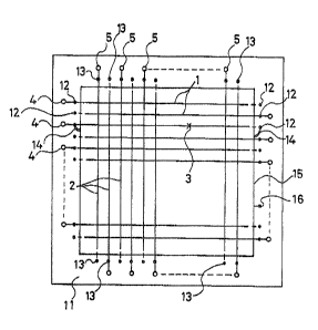
Fig. 3 shows the structure of a matrix address display apparatus
embodying the present invention. The matrix address display apparatus has
2n scanning lines 1 and 2m signal lines 2 which are provided at right angles
to the scanning lines 1. The matrix type display apparatus has, as a
display, a plurality of elements such as liquid crystal cells or
electroluminescence cells on each cross point of the scanning lines 1 and
the signal lines 2, thereby forming a pixel part. Conductive parts 12 are
; 10 provided at both ends of the scanning lines 1. Conductive parts 13 are
provided at both ends of the signal lines 2. A rescue line 15 is provided
surrounding the pixel part.
When one of the lines 1 is "brolcen" at a point 3, the conductive part
12 provided on one end of bro~en scanning line 1 and the rescue line 15 are
connected by a conductor 14 used as a connecting means. The conductive part
12 provided on the other end of broken scanning line 1 and the rescue line
15 are also connected by a conductor 14. Therefore, the signal can be fed
to the broken scanning line 1 through the rescue line 15.
The conductor 14 can be formed by known wirebonding of A1 wire, Au
wire, or the like. In such a case, the conductive parts 12 and 13 used as
bonding pads generally have A1 layers on top, and at least a si~e of about
100 micrometer x 100 micrometer which is sufficient in this embodiment.
Some branch lines 16, which are connected to the rescue line 15, are
preferably provided for use in other embodiments. In the case of using
wire-bonding, the conductive part having A1 layer on top is provided at the
end of the branch line 16.
The rescue line 15 mus~ be provided out of the way of the pixel part
; wherein the pattern of the scanning lines 1 and the signal lines 2 cross and
the display elements are provided. Therefore, it is suitable tha~ the
rescue line 15 be provided between the periphery of electrodes 4, 5 and the
pixel part, since the rescue operation for the broken lines can be carried
out independently of the connectln~ operation of the electrodes 4, 5 and the
outer circuit. It is suitable that the rescue line 15 and the branch line
16 have exposed conductive parts on which the conductor 14 is provided for
rescue. For avoiding short-circuits upon connecting the electrodes 4, 5 and
PAT 11140-1
:.
'., ., ',' .
- ~ ' - ' ~ . ' ' . ' ' . . ' ' ' '
~Z7~3V5
the outer circuit, the peripheral part of the display apparatus 11 must not
have exposed conductive parts other than the electrodes 4 and 5.
Fig. 4 shows a matrix address display apparatus accordlng to a second
embodiment of the present invention. In this embodiment disconnection parts
17 are provided for dividing the rescue line into two rescue lines 18 and
18'. As a result of the dividing of the rescue line, two break points 3 can
be rescued as shown in Fig. 4. Further, the floating capacitances generated
in the cross points of the rescue line and lines 1 and 2 are reduced.
In a third embodiment (not shown), for simplification of the
manu~acturing process, the rescue line is formed simultaneously with the
scanning lines 1 or the signal lines 2. In the case where the scanning
lines 1 and the signal lines 2 are formed on one substrate, an insulating
layer for insulating both lines 1 and 2 is necessary. Therefore, it is easy
to form the rescue line simultaneously with the scanning lines 1 or the
signal lines 2. For obtaining small resistance, the rescue line 18 is snade
of a lower resistance material placed between the signal line and the
scanning line.
Figs. 5, 6A and 6B shows a fourth embodiment of the present invention.
Fig. S is a plan view, Fig. 6A is a sectional view taken along the line A-A'
of Fig. 5, and Fig. 6B is a sectional view taken along the line B-B' of
Fig. S. In Fig. 6A, on a glass substrate 23 an insulating layer 25 is
formed. An insulating layer 20, which has openings 21, is provided on the
insulating layer 25. A conductive connecting line 19 is provided under the
insulating layer 20a between the two openings 21, 21. The signal line 2 is
formed in the openings and on the insulating layer 20. The rescue line 15
is formed on the insulating layer 20a. As described above, the signal
electrode 5 and the signal line 2 are connected and the rescue line 15 is
formed in such a manrler that the rescue line is insulated from the scanning
line 1 and the signal line 2 (Figs. 6A and 6B). The signal line 2 and the
rescue line 15 may be of the same material (e.g. A1) and may be
simultaneously formed. The connecting line 22 between the signal electrode
S and the signal line 2 may not be positioned on top of the substrate.
However, when one part of the connecting line 22 is exposed (provided on top
of the substrate), the exposed part can be used as the conductive part 13
forming a bonding pad for a rescue operation (see Fig. S).
` ~ - 4 -
PAT 11140-1
~ ~7~30S
The insulating layer 20 is simultaneously formed as the insulating
layer for pixel part 24. The conductive connecting line 19 is
simultaneo~lsly formed with the scanning line 1. Therefore, additional
processing is not necessary for forming the insulating layer 20 and the
conductive connecting line 19. The structure shown in Fig. 6A can be
applied to the scanning line 1.
Fig. 7 shows a sectional view of a thin film transistor used in a
matrix address display apparatus according to a fifth embodiment of the
invention. SiO2 film 25 is formed on a glass substrate 23. The scanning
line 1 is used as a gate of the transistor. A gate insulating fil.m 20 of
Si3N4 is formed on the gate 1. Amorphous Si film 26, which includes very
little impurity, is formed on the gate insulating film 20. Numerals 2 and
2' designate Al source-drain wiring. Amorphous Si film 27 doped with a
large quantity of impurity is formed for improving the ohmic contact of the
wiring 2 and 2' and the amorphous Si film 26. A protective film 28 of Si3N4
is formed for protecting the amorphous Si film 26 from the air. The
source-drain wiring 2 operates as the signal line 2 and the source-drain
wiring 2' operates as the wiring 2' for connecting transparent electrodes
such as Indium-Tin-Oxide (ITO) electrodes.
In this embodiment, the gate insulating film 20 is sirnultaneously
formed and is the same material as the insulating layer of Figs. 6A and 6B.
Fig. 8 shows a sectional view of a thin film transistor used in a
matrix address display apparatus according to a sixth embodiment of the
invention. In this embodiment, a protecting film Z9 ls formed for
protecting the amorphous Si film 26 (including li~uid crystal) which forms a
channel region. The protect film 29 can be made from inorganic material
such as Si3N4 or organic material such as polyimide. In this embodiment,
the structure made by the signal line 2, the connecting conductive line 19
and the insulating layer 20 (see Fig. 6A), can be formed by using the signal
lines 2 and 2' and the protective film 29.
Fig. 9 is a partial plan view of a matrix address display apparatus
according to a seventh embodiment of the invention. Fig. lOA is a sectional
view taken along the line A-A' of Fig. 9 and Fig. lOB is a sectional view
taken along the line B-B' of Fig. 9. In this embodiment, the scanning lines
~.
i, ~" ,,
~ - 5 -
- PAT 11140-1
' , ' ' `' ~, ' ~`'. . ;
. . .
.
- ` : ' ~'. ' . :
: ~ ' '" :
~L~743~)~
1 are formed on a substratP 30 and the signal lines 2 are formed on another
substrate 31. The scanning lines 1 and signal llnes 2 are of transparent
conductive film such as IT0. The substrates 30 and 31 are put together with
predetermined gap 32 therebetween wherein the liquid crystal is introduced.
A sealing member 33 is provided between the substrates 30 and 31.
A carbon-rich resin cornposltion 34 is formed on the scanning electrode
4 for connecting the scanning line 1 to the scanning electrode 4. The
insulating layer 20 is formed for insulating the rescue line 15 from the
, scanning electrodes 4 and the signal electrodes 5. For the insulating layer
20, SiO2, Si3N4 or polyimide resin may be used. In the insulating layer 20,
openings are formed for the conductive parts 12 and 13. When one of the
lines 1 or 2 is broken, the conductive parts 12 or 13 are connected to the
rescue line 15, thereby restoring the designed function.
Although the invention has been described in its preferred form with a
certain degree of particularity, it is understood that the present
disclosure of the preferred form can be changed in the details of
construction and the combination and arrangement of parts may be modified
without departing from the spirit and the scope of the invention as
hereinafter claimed.
;~: - 6 -
".,
PAT 11140-1
':~
- :
,
.