Note: Descriptions are shown in the official language in which they were submitted.
3~7
1 This invention relates to apparatus for, and methods
2 of converting binary coded values to analog values with minimal
3 error. More particularly, the invention relates to apparatus
4 for, and methods of, correcting in a digital-to-analog converker
on an integrated circuit chip for second order errors such as
6 result from stresses in the chip.
8 Various types of equipment receive information in
9 analog form. Such equipment includes process control equipment,
measuring instrwments, communications equipment and a wide
11 variety of other equipments. Digital computers and data
12 processing systems often receive input parameters in analog form
13 from such equipments and convert th~se parameters to digital
14 form for processing in the computers or the ~ata processing
equipmentsO After the analog information has been converted to
~6 digi~al information and has been processed, the output
17 infonmation from the digital computers or the data processing
18 equipmen~s is often converted to an analog form. By converting
19 the digital information to an analog form, the user ca~
assimilate the information in ways which would be difficult if
21 the information remained in digital form.
22
23 A good example of the conversions described in the
24 previous paragraph is in the recording and reproduction of
music. The music is p~oduced in analog form. It i~ converted
2~ to digital form by recently developed data processing techniques
27 and is recorded in digital form on a medium such a~ a tape or a
28 disc. When the music i9 to be reproduced, it is converted again
29 to analog orm because this i5 the form which is necessary to
31
~27~
1 operate sound transducers to give meaning to the listener when
2 he hears the music.
4 As digital computers and data processing equipments
have become widespread throughout industry and the office and
6 have even become common in the home, the need for inexpensive,
7 simple and reliable apparatus for converting information between
8 digital and analog forms has become of increasing concern. A
9 considerable effort has been devoted over a period of several
decades to provide converting apparatus which is simple,
11 inexpensive and reliable. In spite of such eforts, the
12 converting apparatus now in use does not meet such criteria.
13
14 The converters now in use are generally disposed in a~
integrated circuit chip. The chips are fabricated such that a
16 plurality of chips (or dies) are simultaneously fabricated on a
17 wafer and are then separated from one another after such
18 fabrication. Each die has a plurality o current sources which
19 are selectively energized in accordance with t~e binary coded
value being converted to the analog value.
21
22 The fabrication of the dies (or chips) on the wafer~is
23 obtained only after the performance on the wafer of a number of
24 operations some of which are at relatively high temperatures.
~5 Such temperatures tend to produce stresses on the wafer. These
m 26 stresses are so prevalent that they even affect the ability o
.
27 the diferent current sources on each individual die to produce
; 28 substantially the same current, when energized, as the other
~ 29 current sources o~ such die. A5 a result, second order errors
`~ 30 are produced in the current sources in each dle~ These second
31
1 order errors affect the ability of the converters formed on such
2 chips (or dies) to provide an accurate conversion to an analog
3 value of binary coded signals introduced to the converter.
Applicant does not believe that anyone prior to
6 applicant has appreciated that second order errors occur in an
7 integrated circuit chip from stresses produced in the chip
8 during the fabrication of the wafer incorporating the chip~
9 This is particularly true since integrated circuit chips now
have an area as small as that defined by a dlmension one quarter
ll of one quarter of an inch (1/4~) on each side. Since no one has
12 apprecia$ed that such second order errors exist in integrated
13 circuit chips, no one can has provided any effective way of
14 compensating for such error. Furthermore, no one can have
provided the particular techniques used by applicant to enhance
16 the accuracy of a converter on an integrated circuit chip in
17 converting a binary coded value to an analog value.
18
19 m e converters now in use are generally disposed on an
integrated circuit chip. The chips are fabricated such that a
21 plurality of chips (or dies) are simultaneously fabricated on a
22 wafer and are then separated after such fabrication. The
23 fabrication of the dies on the wafer is obtained only after the
24 performance of a number of operations some of which are at
relatively high temperatures. Such temperatures tend to produce
26 stresses in the wafer~ These stresses tend to produce second
27 order errirs in the output currenks produced from different
2~ current sources in the integrated circuit chip7
31
~z~
1 This invention provides a converter which overcomes
2 second order errors such as result from stresses in an
3 integrated circuit chip. The invention provides such
4 compensation in a simple and reliable manner so that the second
order errors are substantially eliminated with a minimal amount
6 of additional circuitry on the inte~rated circuit chip.
8 In one embodiment of the invention, an integrated
9 circuit chip has circuitry for converting a binary coded value
to an analog value. The chip includes first and second matrices
11 each defined by a plurality of rows and a plurality of columns.
12 The rows and columns have sources at different positions for
13 producing currents in response to binary signals coding for the
14 binary value. Each row on the first matrix is connected to a
~5 row in the second matrix on a reverse-image basis. E'or example~
16 if each matrix has thirty two (32~ rows, rows 1 and 32 on the
17 first matrix are respectivel~ connected to rows 32 and 1 on the
18 second matrix.
19
~0 The rows on the first and second matrices are
-
21 sequentially selected in a pattern providing particular
22 convergences and divergences of successiYe pairs of such rows il~
23 each of such matrices about the center of the mat:rix as a
24 reference. Such sequential selection provides for eyclic
deviations between the rows in the successiYe pairs in each of
26 the matrices, such progressive convergences and progressive
27 divergences about the center line as a reference. 5uch eyclic
28 deviatlons provide for progressive convergences and then
29 divergences of the rows in each of the successive pairs in each
30 of the matrices. Such progressive convergences and divergences
31
32
7~3~
1 may occur in at least a pair of cycles. When the selection
2 occurs in at least a pair of successive cycles, the selected
3 rows in each matrix in one of the cycles are interleaved with
4 the selected rows in the matrix in the other cycle.
6 Upon the selection of each row in the first and second
7 matrices, the different positions ;n the selected row may be
8 progressively selected. In this way, compensation may be
9 provided on the chip for second order errors such as result from
stresses in the chip.
11
12 In the drawings~
1~
14 Figure 1 is a perspective view of a converter on an
integrated circuit chip for converting binary coded values to
16 analog values and particularly illustrates a pair o~ matrices in
17 the converter for minimizing second order errors from stresses
18 in the chip;
19
Figure 2 is a table schematicalIy illustrating the
21 disposition of a plurality of current source~ in rows and
22 columns in each of the matrices in the converter on the
23 integrated circuit chip;
24
Figure 3 is a table illustrating the sequence~ in
~6 which the current sources in the different row9 on the matrix
27 are activated with progres~ive increases in the magnitude of a
2B binary coded value to be converted to analog value7
29
31
32
~3~
1 Figure 4 is a curve schematically illustrating how the
diference~ in the relative dispositions of successive pairs of
3 the rows in the sequences shown in Figure 3 define cyclic
4 relationship;
6 Figure 5 shows curves which illustrate the relative
7 deviations from a median value in a converter of the prior art
8 and a converter included in a preferred embodiment of this
9 invention; and
11 Figures 6a and 6b schematically illustrate the
12 relative deviations from a median value of the currents produced
13 in the current sources in each row in the converters of the
14 prior art.
~6 In cer~ain types of converters for converting binary
17 coded values to analog values~ a plurality o current sources 10
18 (Figure 2) are disposed on an integrated chip~ generally
19 indicated at 12, in a matrix relationship defined by row~ and
columns. In a simple form of converter, eaah progressive one of
21 the current sources 10 in the ~irst row is activate~ for
22 progressive increases in a binary coded value. After all of the
23 current sources ln in the first row have been activated~ the
24 current sources in the next row are progressively actiYated for
progressive incr~a~e~ in the binary value. In this way, the
26 current source~ in the progressive rows are sequentially
27 activated with progres~ive increases in the binary coded value.
28 The current~ in the activated current sourc~ are then summed at
Z9 each in~tant to provide a current with a magnitude lndicative of
the analog values at that instant.
31
43~
l A prior art converter constructed in accordance with
2 the discussion in the previous paragraph is shown schematically
3 in Figure 3 and is designated in that Figure as "prior art
4 converter". As shown in Figure 3, the different rows of the
current sources in such converter are designated by arabic
6 numerals such as "1", "2" and "3". The sequence of activiating
7 the prior art converter in the different rows is indicated by
8 the sequence of the numbers in such converter in Figure 3.
Although integrated circui~ chips are quite small
ll (e.g., 1/4" x 1/4" in area), it has been founcl that the
12 characteristics of the current sources on the chip are not
13 uniform. For example, the thickness of the layers of the
14 semi-conductor material defining the diferent electrodes in the
current sources have not been uniform. This non-uniformity has
16 tended to vary with progressive positions along the area of the
17 chips. These non-uniformities have affected the magnitudes of
18 the currents produced by the current sources at different
19 positions on the integrated circuit chip. These
non-uniformities have caused differential errors to be produced
21 in the chip with progressive increases in the binary coded
22 value to be converted to the analog value.
23
24 Various improvements have been made in converters of
the type discussed in the previous para~raph -to reduce the
26 differential non-linearities of such converters with progressive
27 increases in the binary coded value. For example, one (1)
28 United States patent and one (1) Canadian application assigned
29 of record to the assignee of record of this application are
effective in reducing the differential non-linearities oE a
31 converter disposed on an integrated circuit chip. United
32
7 -
l States Patent No. 4,658,240 issued on April 14, 1987, in the
2 name of James A. Bixby for "Apparatus or Converting Data
3 Between Analog and Digital Values". Canadian application Serial
4 No. 538,297 was filed on July 17, 1887, in the name of Lanny L.
Lewyn for "New Centroiding Algorithm for Networks Used in A/D
6 and D~A Converters". The United States patent discloses and
7 claims a particular re-arrangement of the current sources on an
8 integrated circuit chip for minimizin~ the effects of -the
9 differential non-linearities of the current sources on the chip.
The Canadian application discloses and claims a duplication of
ll the current sources on a chip in a reverse image arrangement to
12 minimize differential non-linearities on the chip.
13
14 Applicant has found that there are, on an integrated
15 circuit chip, second order errors resulting from stresses
. : .
16 produced in the chip, particularly during the steps in which the
17 integrated circuit chip is being treated at elevated
18 temperatures. These stresses cause the current sources at
19 different positions on the chip to produce deviations from a
desired current even when the physical characteristics of these
21 current sources, such as the layers of the materials defining
22 the current sources, are substantially constant.
23
24 Figure 6a illustrates the patterns of the currents
produced by the current sources in the different rows of a
26 converter of the prior art and by the individual currents in
27 each row. The current sources in each individual row are
28 indicated at a different heighth in Figure 6a than the current
29
31
.
'~ !.
- 8 - ,
~2~
1 sources in every other row. The differenk currenk sources in a
2 row are indicated at progressive positions along the row in
; 3 Figure 6a. In Figure 6a, currents produced in each current
4 source in a row above a median value are indicated by a dark
back~round and currents produced in each current source in a row
6 below the median value are indicated by a light background.
8 Figure 6b illustrates the cumulative value of the
9 current in each of the rows shown in Figure 6a~ In Figure 6b,
each of the different ro~s in the converter on the integrated
11 circuit chip is at the same vertical position as the
12 representation shown in Figure 6a. As wilI be seen, the
13 cumulative current in the current sources in each of the rows in
14 the upper half of Figure 6b deviate only slightly from a median
position. However, the cumulative current in the current
16 source~ in each of the rows in the lower half of Figure 6b
17 deviate considerably from the median of the cumulative currents
18 in the rows in the upper half of ~igure 6a. Furthermore, the
: 19 cumulative current in the current sources in the rows in the
lower half of Figure 6b tend to decrease progressi~ely with
21 progressive positions downwardly in Figurq Sb.
22
23 Figures 6a and 6b represent measurements taken on an
24 actual unit of an integrated circuit chip providing in the prior
art a conversion between binary coded value~ and analog values.
26 Figures 6a and 6b are only illustrative~ An analysis of a
27 number o other units has indicated similar problem~. The
28 patterns in these ~hip~ may not be identical to those shown i~
29 F;gures 6a and 6b but they tend to show that there is a
dissimilarity in the patterns of the cumulative currents in ~he
31
~L~r~3~-~
1 rows on one half o the chip relative to the patterns of the
2 cumulativ~ currents in the rows on the other half of the chip.
3 The dissimilarities in the patterns of the cumulative currents
4 in the rows o~ the two (2) halves of the chips tend to result
from stresses produced in the chip during the steps of
6 fabricating the chips, particularly the step~ involving heating
7 ~he chip to high temperaturesA
9 This invention provides a converter which overcomes
the second order errors resulting from stres~es in an integrated
11 circuit chip on which the converter is formed. In one
12 embodiment of the invention, an integrated circuit chip
13 generally indicated in broken lines at 20 tFigure 1) may be
14 fonmed in a conventional sequence of steps to respond to a
plurality of binary coded signals to be converted to an analog
~6 value.
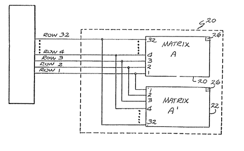
17
18. The in~egrated circuit chip 20 include~ a pair of
19 matrices 22 (A) and 24 (A1) on the chip. Each of the matrice~
22 and 24 is formed from a plurality o current source~ 26
21 (such as the current sources 10 in Figure 2) disposed in rows
22 and columns.; For eY.ample, there may be thirty two (32) rows o~
~3 curr~nt sources 26 in each o~ the matrices 22 and 24, ~hese
24 row~ may be respectively designaked as "1~ through ~32no Each
.
:: 25 of the rows may ~ave a plurality o current sources 26 at
26 progressive positions along the row. I~ this respect, each of
27 the matrice~ 22 and 24 corre~ponds in general format to the
:
~:` Z~ matrix shown in Figure 2 and d~scrîbed above.
29
. 30
31
~2~ 7
1 The current sources 26 in each of the rows in the
2 matrix 22 is connected on a reverse-image basis to the current
3 sources in one of the rows of the matrix 24. For example, the
4 current sources 26 in the row 1 in the matrix 22 ar~ connected
to the current sources in the row 1 in the matrix 24.
6 Similarly, the current sources 26 in the row 32 in the matrix 22
7 are connected to the current sources in the row 26 in the matrix
24. As will be seen, the row 1 is at the bottom of the matrix
9 22 and the top of the matrix 24. Similarly, the row 32 is at
the top of te matrix 22 and at the bottom of the matrix 24.
11 .
12 The different rows in the matrices 22 and 24 are
13 activated in a particular pattern to minimize second order
14 errors resulting from stres~es in the integrated clrcuit chip
20. Preferably the rows in each matrix are activated so that
~6 the differences between successive pairs of activated rows in
17 such matrix have a cyclic relationship relative to the center of
1~ the matrix as a reference. For example, a preferred arrangement
19 for activating progressive pairs of rows in the ~atrix 22 is
shown as the first embodiment in Figure 3. In the preferred
21 arrangement, progressive pairs of rows in the matrix 2~ are
2Z ~equentially a~tivated as follows: (1) 15 and 20, ~2) 11 and
23 24, (3) 7 and 28 and (4j 3 and 32.
24
As will be seen, the rows 15 and 20 in the matrix 22
26 are disposed on the oppo~ite sides of the center o the matrix
27 as a reference. The row~ 11 and 24, the rows 7 and 28 and the
28 row~ 3 and 32 are al50 disposed on opposite sides of the center
29 of the matrix 22 as a reference~ m e rows 7 and 28 are further
from the center of the matrix 2~ than the rows 15 and 20/ and
31
~2~ 7
l the rows 3 and 32 are further from the center of the matrix 22
2 than the rows 7 and 28. Furthermore, thP rows 15 and 20, the
3 rows 11 and ~4, the rows 7 and 28 and the rows 3 and 32
4 progressively deviate from the center of the matrix 22.
~ In each of the first pairs in the preferred embodiment
7 of the invention, the first row in the pair has a lower number
8 than the second row in the pair. However, in successive pairs
9 of rows in the preferred embodiment, the first row in the pair
has a higher number than the second row in the pair. This may
ll be seen from the following progressive pa;rs of rows in the
lZ preferred embodiment: (S) 18 and 13, (6) 22 and 9, (7) ~5 and 5
13 and (8) 30 and 1. The rows in each of the pairs (5)~ (6), (7)
14 and (8) in each matrix are on opposite sides of the center o~
the matrix. The rows in the successive pairs (5~, (6)~ (7) and
16 (8) deviate progressively from the center of the matrix 22.
17
18 In the preferred embodiment, progressive pairs of rows
l9 are subsequently activated in a pattern similar to that
discussed two paragraphs previously~ These progressi~e pairS
21 are as follows: (9) 16 and 19, (10 12 and 23, (11) 8 and 27 and
22 (12) 4 and 31O As will be seen~ the rows in each of the pairs
23 (9), (10~, (11) and ~ in each matrix are on opposite sides of
. .
24 the center of the matrix. The rows in the successive pairs in
each matrix deviate progressively from the center of ~he matrix.
26 Furthermore, the rows ~n the pairs designated as ~9), (10), ~
27 and (12) are respectively interleaved with the rows desi~nated
28 as (1), (2), (3) and (4~.
29
31
,
~27~L3~7
l Similarly, the remaining pairs of rows for each matrix
2 in the preferred embodiment of the invention are respectively
3 desi~nated as (13) 17 and 14, (14) 21 and 10, (15) Z5 and 6, and
4 (16) 29 and 20 The rows in each of the pairs (13), (14), (15)
and (16) for each matrix are disposed on opposite sides of the
6 center of the matrix. The rows in each of the successive pairs
7 (13), (14), (15) and (16) in each matrix deviate progressively
8 from the center of the matrix~ The rows in these remaining
9 pairs in each matrix are respectively interleaved with the rows
in the pairs defined as (5), (6), (7) and (8) for that matrix.
11
lZ As will be seen rom the progressive pairs of rows in
13 the preferred embodiment and from the discussion above, the
14 the progressive pairs of rows in each matri~ preferably have a
converging or diverging pattern relative to the center of the
l6 matrix. Thi5 pattern may converge or diverge initiall~ in a
17 first direction relative to the center o each ~atrix uch as a
l8 negative direction and then converge or diverge in an opposite
19 direction such as a positive direction relat;ve to the center of
the matrix. Furthermore, this diverging or converging pattern
21 is preferably cy~lic or repetitive for each matrix as indicated
22 at 30 in Figure 4. When the pattern is cyclic or repetitive for
23 each matrix, the progressive pairs of rows in one cycle or
24 repetit;on for such matrix may be interleaved in the matrix with
the progressive pairs of rows in another cycle or repeti~ion.
26
27 Figure 3 illustrates the pattern~ constituting other
2~ embodiments of this inYention for sequentially activating pairs
29 of rows on one of the matrice~ sus~h as the matrix 22. Although
30 these other embodiments provide results superior to those
31
3~
1 prsvided in the prior art, they do not appear to minimize second
2 order errors with qu;te the same effectiveness as the preferred
3 embodiment. However, each of these other embodiments is similar
4 to the preerred embodiment in activating progressive pairs of
rows in a particular pattern in each matrix and in providing the
6 particular pattern with cyclic or repetitive characteristics
7 relative to the center of the matrix as represented by an
8 interleaved relationshlp between the progressive pairs in the
9 different cycles or repetitions.
11 As will be appreciated, when each of the rows in each
12 of the matrices 22 and 24 is activated, progressive ones of the
13 current sources 26 in the activated row in such matrix is
14 energized for progressive increases in the binary value coded by
the binary signals. The particular pattern of energizing the
~6 different current sources 26 in the activated row in each matrix
17 is not Lmpo~tant in this invention. For example, the current
18 sources 26 progressively disposed along the activated row in
19 each of the matrices 22 and 24 may be sequentially activated for
progressive increases in the binary value coded by the binary
21 signals i~troduced to the converter.
22
23 Flgure S illustrates h~w the converter of this
24 invention minimizes second order errors such as result from
stresses in an integrated circuit chip~ In Figure 5~ a curve 40
26 is i~cluded to show the deviations from a desired value (the
27 zero zxis in Figure 53 ~n the cumulatiYe current produced in
28 each row in a converter of the prior art. In the curve 407 ~he
29 progressive rows activated in the sequence are indicat~d by
arabic numbers below the progressive increments in the curve.
31
32
~2~43~L7
As will be seen in the curve 40, such a deviation is indicated
2 for each row by a step such as a step 42 for the row 5. It will
3 also be seen that the rows in the converter of the prior art are
4 activated sequentially from row 1 to row 32. The area between
the curve 40 and the zero (0) axis represents the cumulative
6 dèviation of the cumulative currents in the rows 1 through 32.
8 Figure 5 also includes a curve 50 showing the
9 deviations from a desired value when the matrices 20 and 22 are
paired as shown in Figure 1 and discussed above and when the
11 rows in the matrix 22 are activated in a sequential pattern
12 identified by the preferred embodiment in Figure 2. This
13 pattern is also indicated by arabic numberals above the
14 successive steps or increments in the curve S0. As will be
seen, the deviation from a desired value represented by the zero
~6 (03 axis are considerably reduced for each of the rows below the
17 deviations for the different rows in the curve 40 for the
18 converters of the prior art. It will be appreciated that the
19 wire 50 represents the errors otained in the matrices 22 and 24
by pairing the differe~t rows in the matrices on a reverse-
21 image basis as described in detail above.
22
23 Although this invention has been disclosed and
24 illu~trated with ref~rence to particular embodiment~, the
principles involred are susceptible for use in numerous other
26 embodiment~ which will be apparent to persons skilled in th~
27 art. The invention is, therefore, to be limi~ed only as
28 ~ndlcated by the scope of the appended ~laims.
29
31