Note: Descriptions are shown in the official language in which they were submitted.
~.X~!~;9~L
PHN.11.618 1 27.10.86
Arrangement for full-duplex data transmission
over two-wire circuits.
(A) Backqround of the invention
The invention relates to an arrangement for full-
duplex data transmission over a two-wire circuit, said
5 arrangement comprising a one-way transmit channel connected
to a baseband data transmitter, a one-way receive channel
connected to a baseband data receiver, a hybrid junction for
interconnecting the transmit and receive channels and the two-
wire circuit, an echo canceller comprising an adaptive filter
with adjustable filter coefficients and an adjusting circuit
for the filter coefficients, and a combining circuit inserted
in the receive channel, the adaptive filter generating an
approximated echo signal from signals in the transmit channel,
the combining circuit differentially combining the approxim-
ated echo signal with incoming signals of the receive channel
to generate a residual signal and the adjusting circuit,
in response to signals in the transmit channel and the
residual signal in the receive channel, adjusting the adaptive
filter coefficients to minimize a predetermined function of
20 the residual signal.
A similar arrangement is known from the article
by P.J. van Gerwen et al. in IEEE J. Select, Areas Commun.,
Vol. SAC-2, No.2, March 1984, pp.314-323.
For the full-duplex data transmission use is often
25 made of the circuits of the public telephone network. In the
local network the circuits are usually of the two-wire type.
Data transmission is then subject to four main types of
impairments: echo signals, intersymbol interference, cross-
talk from ever present signals in adjacent wire-circuits and
30 noise (background noise and impulse noise). Many of the
arrangements available now for full-duplex data transmission
over two-wire circuits comprise an echo canceller with an
adaptive filter to considerably reduce the disturbing effect
'' '. ' ~ . ~ ' '
' ' ~ .
~27~59A
PHN.11.618 2 27.10.86
of echo signals, the adaptive filter coefficients being
usually adjusted iteratively according to a criterion for
minimizing the mean square value of the remaining echo in the
residual signal. The data receivers utilized in these
5 arrangements further comprise the current arrangements for
strongly reducing the disturbing effect of intersymbol
interference, ever present crosstalk and background noise.
However, in the arrangements known thus far no specific
precautions have been taken to reduce the influence of impulse
noise consisting of concentrated pulse-like disturbances
occurring at irregular intervals and usually far apart.
The influence of this impulse noise is particularly felt in
longer circuits operating at higher data rates.
A possibility to combat the effect of impulse noise
known E~ _ is the insertion of a smearing filter at the
transmit end and a complementary smearing filter ~also
referred to as desmearing filter) at the receive end of the
circuit. The two filters generally have a flat amplitude
characteristic, but their group delays vary in the prescribed
20 freqvency band in a contrary fasion, the sum of the group
delays being made as flat as possible. In the ideal case,
a data signal passing through the two filters merely
experiences a delay. A noise impulse injected into the
channel, however, passes only the complementary smearing
25 filter at the receive end so that the energy of such a noise
impulse is smeared in time and, consequently, its effect on
the received data signal may be decreased at any moment.
Further details about the design and implementation of
efficient and yet simple smearing filters for data trans-
30 mission can be found in the article by G.F.M. Beenker et al.in IEEE Trans. Comm., Vol. COM-33, No.9, September 1985,
pp.955-963.
In the arrangement for full-duplex data transmission
over two-wire circuits, the effect of impulse noise can be
35 combatted in the same manner byconnecting the data trans-
mitter _ a smearing filter to the input of the one-way
transmit channel and by connecting the data receiver via a
PHN.11.618 3 27,10.86
complementary smearing filter to the output of the one-way
receive channel. This way of connecting the smearing filters
implies that the signals in the transmit channel applied to
the echo canceller are now formed by smeared data signals
having a considerably greater number of significant signal
values than would be the case without smearing filters.
This also results in a considerably more complicated
implementation of the echo canceller as the signal samples
to be applied to the digital echo canceller have to be
represented with a far greater number of bits. This is an
undesired effect, more specifically in view of the expectation
that smearing filters need only be used for a limited number
of circuits in the local telephone network, so that the
complexity of the echo canceller present in each two-wire
circuit is of far greater importance than that of the smearing
filters, which should be considered an option not applied
relatively frequently.
(B) SummarY of the invention
The invention has for its object to provide an
arrangement for full-duplex data transmission of the type
set forth in the preamble of paragraph (A), in which smearing
filters are applied without increasing thereby the complexity
of the echo canceller.
The arrangement according to the invention is
characterized in that the arrangement comprises first delay
means inserted in a first signal path from the data trans-
mitter output to the adjusting circuit, and second delay
means $nserted in a second signal path from the data trans-
30 mitter output via the adaptive filter and the combiningcircuit to a point in the receive channel where the residual
signal to be applied to the adjusting circuit is tapped from
the receive channel, the first and second delay means having
a same delay substantially corresponding to the signal delay
of the cascade connection of the smearing and complementary
smearing filter, and the complementary smearing filter having
been inserted in the receive channel between the hybrid
junction and said tapping point for the residual signal.
127~9~
-3a- 20104-8215
In accordance with the present invention, there is
provided an arrangement for full-duplex data transmission over
a two wire circuit, said arrangement comprising a one-way
transmit channel connected to a baseband data transmitter and
including a smearing filter, a one-way receive channel con~
nected to a baseband data receiver and including a complemen~
tary smearing filter, a hybrid junction for interconnecting the
transmit and receive channels and the two~wire circuit, an echo
canceller comprising an adaptive filter with adjustable filter
coefficients and an adjusting circuit for the filter
coefficients, and a combining circuit inserted in the receive
channel, the adaptive filter generating an approximated echo
signal from signals in the transmit channel the combining
circuit differentially combining the approximated echo signal
with incoming signals of the receive channel to generate a
residual signal and the adjusting circuit, in response to
signals in the transmit channel and the residual signal in the
rece~ve channel, adjusting the adaptive filter coefficients so
as to minimize a predetermined function of the residual signal,
characterized in that the arrangement comprises fir~t delay
means inserted in a first signal path from the data transmitter
output to the adjusting circuit, and second delay means
inserted in a second signal path from the data transmitter out~
put via the adaptive filter and the combining circuit to a
point in the receive channel where the residual signal to be
applied to the adju~ting circuit is tapped from the receive
., ". .. .
.''~ ~' . ` ' .
- ,
'. ~ ' ~ -
1274~i94
-3b- 20104-8215
channel, the first and second delay means having a same delay
substantially corresponding to the signal delay of the cascade
connection of the smearing filter and the complementary smear-
ing filter, and the complementary smearing filter having been
inserted in the receive channel between the hybrid junction and
6aid tapping point for the residual signal.
~2~74~i9A
PHN.11.618 4 27.10.86
~C) Short description of the drawinqs
Embodiments of the invention and their advantages
will now further be explained with reference to the drawings
in which:
Fig. 1 shows a block diagram of a prior art
arrangement for full-duplex baseband data transmission over
two-wire circuits, the arrangement being provided in a known
manner with smearing filters to combat the effect of impulse
noise;
lo Fig. 2 shows a block diagram of a first embodiment
of an arrangement according to the invention for full-duplex
base-band data transmission over two-wire circuits;
Flg. 3 shows three block diagrams of practical
modiflcations of the arrangement of Flg. 2 as regards the
connection of the echo canceller to the transmit channel;
Fig. 4 shows a block diagram of a second embodiment
of an arrangement according to the invention for full-duplex
base-band data transmission over two-wire circuits;
Fig. 5 shows a block diagram of a variant of the
arrangement of Fig.4 leading to a simpler implementation;
Flg. 6 shows a block diagram of a passband variant
of the first embodiment of an arrangement according to the
inventlon shown in Fig.2, which variant is arranged for full-
duplex passband data transmission over two-wire circuits;
Fig. 7 shows a block diagram of a passband variant
of the second embodlment of an arrangement according to the
invention shown in Fig.5, which variant is arranged for full-
duplex passband data transmission over two-wire circuits, and
Flg. 8 shows a block diagram of a variant of the
arrangement of Fig.7, in which smearing filters of the base-
band type have been applied.
(D) DescriPtion of the embodiments
D(1), General descriPtion
In Fig. 1 the block diagram is represented of a
known arrangement for full-duplex baseband transmission
:`' . , ', ' : '.-: ' '
, .
.'~ . -. ~. ~ , .
.
- . ~ .
~2~ 4
PHN.11.618 5 27.10.86
of binary data signals over a two-wi~e circuit 1 in the
public local telephone network~
This arrangement comprises a one-way transmit
channel 2, a one-way receive channel 3 and a hybrid junction
4 with a compromise balancing network 5 to interconnect these
channels 2, 3 and two-wire circuit 1. A baseband data trans-
mitter 6 is connected to transmit channel 2 and comprises a
data source 7 and a line encoder 8 converting a binary
data signal from data source 7 into a ternary data signal in
accordance with the AMI code (Alternate Mark Inversion) for
obtaining a line signal suitable for transmission over two-
wire circuit 1. Via hybrid junction 4 and two-wire circuit 1
this line signal is transmitted to a remote arrangement not
shown in Fig. 1, but implementated in the same manner. A line
slgnal derived from this remote arrangement is transmitted
over two-wlre circult 1 and applied via hybrid junction 4
to recelve channel 3 and passed on therein to abaseband data
recelver 9 via a receive filter 10. Data receiver 9 comprises
a line decoder 11, a detector 12 for the data signal thus
obtained and a data sink 13 to which the detected binary data
signal is applied. Data receiver 9 may also contain an
equalizer (not shown in Fig.1) at the input of line decoder
1 1 .
As the impedance of two-wire circuit 1 ls not
exactly known in practice, hybrid junction 4 is not perfectly
termlnated by compromise balancing network 5. This leads to
a direct leak from transmit channel 2 to receive channel 3
via hybrid junction 4. In addition, impedance discontinuities
in two-wire circuit 1 lead to signal reflections. Botheffects
lead to echoes of the data transmitter 6 output signal
appearing in receive channel 3.
To reduce the disturbing effect of these echo
signals as much as possible, the arrangement of Fig.1 is
provided with an echo cancelller 14 which comprises an
adaptive filter 15 with adjustable filter coefficients and
an adjusting circuit 16 for these filter coefficients.
In response to the line signal ln transmit channel 2 this
.
,: ~ ., . . , -
:
. . .
;9~
PHN.11.618 6 27.10.86
adaptive filter 15 generates an approximated echo signal
which is subtracted, in a combining circuit 17, from the
incoming signals of receive channel 3 (the received line
signal from the remote arrangement, disturbances and the
5 echoes of the line signal in transmit channel 2). At the
output of combining circuit 17 a residual signal will then
appear which is substantially echo-free and which is applied
to data receiver 9.
In response to the line signal in transmit channel
l 2 and the residual signal in receive channel 3 the adjusting
circuit 16 ad~usts the filter coefficients of adaptive
filter 15 so as to minimize a predetermined function of
this residual signal. Usually this predetermined function
is the mean square value of either the residual signal itself
or an odd, non-decreasing function of the residual signal.
The optimal adjustment of the filter coefficients is
iteratively obtained with the aid of a gradient-type
algorithm. Further details about the design and p~ssible
implementation of digital versios of echo canceller 14 and
also of data receiver 9 are discussed in the aforesaid
article by P.J. van Gerwen et al and the references
mentioned therein.
However, especially in longer wire-circuits and
at higher data rates, data transmission is also disturbed
by a type of impairment known as impulse noise. This impulse
noise consists of concentrated pulse-like disturbances
occurring at irregular intervals and usually far apart.
It is a known fact that the effect of the impulse noise can
be combatted by inserting a smearing filter at the transmit
end of the circuit and a complementary smearing filter at
the receive end. In the arrangement represented in Fig.1
use is made of this known measure by connecting data
transmitter 6 via a smearing filter 18 to the input of
transmit channel 2 and data receiver 9 via a complementary
smearing filter 19 to the output of receive channel 3.
The use of the smearing filters 18, 19 in the
arrangement of Fig. 1, however, results in the line signal
~2~7~L594
PHN.11.618 7 27.10.86
in transmit channel 2 applied to the echo canceller 14 being
now formed by a smeared data signal with a considerably
greater number of amplitude levels than the three levels of
the ternary data signal at the output of line encoder 8.
Consequently, the implementation of echo canceller 14 becomes
considerably more complex, as in that case much higher
demands are to be made on the accuracy with which the signal
to be applied to the echo canceller 14 is represented inter-
nally in echo cance].ler 14; thus in a digital embodiment of
echo canceller 14 this means a representation with a far
greater number of bi,ts than the two bits required for the
representation of the ternary data signal at the output of
line encoder 8. The strongly increased complexity of echo
canceller 14 has a particularly undesired effect as it is
expected that the smearing filters 18, 19 need only be
introduced in a relatively small number of two-wire circuits
of the local telephone network, making the complexity of the
echo canceller 14 at each two-wire circuit of far greater
importance than the complexity of the smearing filters 18, 19,
wich can be considered an option applied rather infrequent.ly.
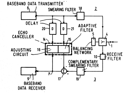
D(2) First emhodiment of the invention
Fig, 2 shows the block diagram of a first embodiment
of an arran~ement in accordan.ce with theinvention, wherein
elements corresponding with elements in Fig. 1 are represented
by the same reference numerals as in Fig. 1.
This arrangement comprises first delay means 20
inserted in a first signal path from the output of data
transmitter 6 to the input of adjusting circuit 16 of echo
canceller 14 and further comprises second delay means 21
inserted in a second signal path from the output of data
transmitter 6 via adaptive filter 15 of echo canceller 14
and combining circuit 17 to a point P in receive channel 3
where the residual signal to be applied to adjusting circuit
16 is tapped from receive channel 3. These first and second
delay means 20, 21 have the same delay D substantially
corresponding to the signal delay S of the cascade connection
-
~2~4594
PHN.11.618 8 27.10.86
of smearing filter 18 and complementary smearing filter 19.
Complementary smearing filter 19 has further been inserted
in receive channel 3 between hybrid junction 4 and the said
tapping point P for the residual signal. In the embodiment
shown in Fig.2, the second delay means 21 have been inserted
in that part of the second signal path which is situated
between the output of data transmitter 6 and the input of
adaptive filter 15 and the complementary smearing filter has
been inserted between hybrid junction 4 and combining
10 circuit 17.
The effect of the application of these measures
is that adaptive filter 15 and adjusting circuit 16 of echo
canceller 14 receive signals from transmit channel 2 which are
formed by delayed versions of the ternary data signal at the
15 output of data transmitter 6 and, consequently, not by the
smeared data signal at the output of smearing filter 18 as
in the arrangement of Fig.1. Thus the signals to be processed
ln the echo canceller 14 can be represented with the same
degree of accuracy as when the smearing filters 18, 19 are
20 not utilized, that is to say with a digital implementation of
echo canceller 14 again with the two bits required for the
representation of the ternary data signal at the output of
data transmitter 6. In addltion, it turns out that it will
suffice that the impulse response of adaptive filter 15 in
25 echo canceller 14 has the same length as in the case without
the application of smearing filters 18, 19, despite the
fact that the echo signal path now also includes the smearing
filters 18, 19. This will be further explained for the case
that adaptive filter 15 and smearing filters 18, 19 are
30 transversal filters of the time-discrete type and thus
equipped for processing signals whose samples occur at
instants t = nT, where n is an integer with -~~n~O and
T is the sampling period. For convenience it is assumed that
the sampling period T equal$zes the symbol period of the data
35 signals. It is ~urther afisumed that only data transmitter 6
ls in operatlon and, consequently, that there is no line
signal from the remote transmission arrangement and no impulse
noise.
~',
;
:', - '
.
, , .
., .
i274~94
PHN.11.618 9 27.10.86
When the samples of the ternary data signal
occurring at instant t = nT at the output of data transmitter
6 are indicated by x(n) and the samples of the echo signal
and the approximated echo signal occurring at instant t = nT
at the inputs of combining circuit 17 by e(n) and e(n),
respectively, and when in a similar manner for smearing filter
18, complementary smearing filter 19, echo path between the
output of transmit channel 2 and the input of receive channel
3, and adaptive filter 15 the values of their impulse
l response at instant t = nT are indicated by sm(n), dsm(n),
g(n) and g(n), respectively, then it holds that:
e(n) = (dsm x g x sm x x) (n) (1)
where the symbol "x" indicates the linear convolution
operator and thus ~dsm x g x sm x x) the linear convolution
of the impulse responses dsm(n), g(n), sm(n) and x(n).
Formula (1) can be rewritten as:
e(n) = ((sm x dsm) x (g x x)) (n) (2)
In the ideal case, the cascade connection of the smearing
filters 18, 19 should only introduce a mere signal delay S
over a number of No sampling periods, so that:
S No
and this cascade connection should then have an impulse
response h(n) with:
h(n) = (sm x dsm) (n1 (4)
for which it holds that:
h(n) = 6(n - No) (5)
where 6 (.) is the Kronecker delta function. However, in
practice the smearing filters 18, 19 are not exactly
complementary so that:
h(n) = &(n - No) + b(n) (6)
where b(n) is the deviation from the ideal situation and
represents the intersymbol interference introduced by the
cascade connection of smearing filters 18, 19. With the aid
of formulae (4) and (6), formula (2) can be written as:
e(n) = (g x x) (n - No) + (b x g x x) (n) (7)
It ls now assumed that the cascade connection of smearing
filters 18, 19 introduces such a small intersymbol
. .
. .. . ~
'-
.
12~
PHN.11.618 10 27.10.86
interference b(n) that the second term in formula ~7) may be
disregarded. In that case it holds with a good approximation
that:
e~n) = (g x x) (n - No) (8)
5 With a delay D of second delay means 21 equal to the cascade
connection of smearing filters 18, 19 and thus with:
D O
adaptive filter 15 will receive input signal samples
x(n - No) and for the samples ê(n) of the approximated echo
signal it holds:
ê(n) = (g x x) (n - No) (10)
For the samples r(n) of the residual signal at the output of
combining circuit 17 output, in the aforesaid assumptions
exclusively formed by the samples of the residual echo signal
the following holds:
r(n) = e(n) - ê(n) = (g x x) (n - No) -
- (g x x) (n - No) (11)
or:
r(n) - ((g - g) x x) (n - No) (12)
As the echo canceller 15 is designed for minimizing the mean
square value of the residual signal, this minimizing will
on account of formula (12) lead to the convergence of the
impulse response g(n) of adaptive filter 15 to the impulse
response g(n) of the echo path between the output of transmit
channel 2 and the input receive channel 3. However, this same
convergence will also take place in case no smearing filters
18, 19 are applied.
Thus, the measures described enable smearing
filters 18, 19 to be utilized without causing any changes in
echo canceller 14 to be effected.
The diagrams of Fig.3 show practical modifications
of the arrangement of Fig.2 as regards the connection of echo
canceller 14 to transmit channel 2.
In the diagram of Fig. 3a the functions of first
and second delay means 20, 21 of Fig. 2 are jointly performed
by delay means 22 common to the first and second signal paths,
which delay means are inserted between the output of data
,
' . ' -- ' , :
.
:
~27~5~4
PHN.11.618 11 27.10.86
transmitter 6 and the two interconnected inputs of echo
canceller 14 for signals originating from transmit channel 2.
In the example under discussion line encoder 8 of
data transmitter 6 is an AMI-coder. The diagram of Fig . 3b
5 shows how in that event the measures described can be com-
bined with measures disclosed in the United States Patent
No. 4,117,277 to simplify the implementation of the echo
canceller 14. In the line encoder 8 of Fig. 3b , which is
known E~ se, the binary data signal from data source 7 is
converted into a modified binary data signal by adding
modulo-2 with the aid of a modulo-2 adder 24 the binary data
signal and the modified binary data signal which has heen
delayed over a time T by means of a delay circuit 23.
The modified binary data signal is further converted into a
lS ternary data signal by linearly subtracting the modified data
binary data signal delayed over a time T from the modified
binary data signal by means of combining circuit 25. This
ternary data signal at the output of combining circuit 25
forms the normal output signal of data transmitter 6 which
is applied to smearing filter 18. Fig. 3b differs from Fig.3a
in that the signal to be applied to echo canceller 14 via
delay means 22 is not formed by this normal output signal of
data transmitter 6, but in accordance with the aforementioned
Patent is formed by the modified binary data signal at the
output of modulo-2 adder 24 which is transferred to an a
additional output of data transmitter 6. The simplification
of the structure of the echo canceller 14(achieved by these
measures the canceller input signal only needs to be repre-
sented with one bit instead of the two bits required in case
of a ternary data signal) is thus retained when smearing
filters 18, 19 are applied.
In the case of transversal smearing filters 18, 19
of the time-discrete type, the elemen~ already available
in smearing filter 18 can also be utilized for realizing the
delay 22. As depicted in the diagram of Fig. 3c, such a
smearing filter 18 comprises a shift register 18(1) connected
to data transmitter 6 and formed by the series connection of
~274~9A
PHN.11.618 12 27.10.86
a number of sections each having a delay T, and a weighting
circuit 18 (2) connected to taps of the sections of the shift
register 18 (1 ) for multiplying the tapped signals by filter
coefficients and summing the resulting product signals,
the sum signal forming the smeared data signal to be applied
to hybrid junction 4. In Fig. 3c the sections of shift
register 18(1) are likewise used to obtain the required delay
D = NoT of delay means 22 by connecting the output of a
certain section ~o the two inputs of echo canceller 14 for
signals originating from transmit channel 2. In a design of
the transversal (smearing filters 18, 19 as proposed in the
aforesaid article by G.F.M. Beenker et al., the value No can
be equal to the number (N - 1) of the sections of the shift
register 18(1) in smearing filter 18. The overall delay of
the sections between the first and the last tap will then be
(N - 1)T, so that the required delay NoT = (N - 1)T can be
obtalned by connecting the output of shift register 18(1)
to echo canceller 14. In the event of No exceeding (N - 1),
the shift register 18(1) should be lengthened by one or more
delay sections 18(3), as indicated in Fig. 3c, and the output
of the thus lengthened shift regsister 18(1) should be
connected to the echo canceller 14. If, in contrast thereto,
No were smaller than (N - 1), the output of a section
precedlng the last section of the shift register 18(1)
should be connected to echo canceller 14.
So far the delay D of delay means 20, 21 and 22
has been chosen equal to the signal delay S = NoT of the
cascade of smearing filters 18, 19. The intersymbol inter-
ference (b x g) (n) introduced by the cascade of these
filters 18, 19 and the echo path falls partly within the
interval of the impulse response of the actual echo path
delayed over No sample periods g(n - No) and this part is
likewise cancelled by echo canceller 14, as the interval of
impulse response g(n - No) of adaptive filter 15 equals that
of q(n - No)~ In some instances, a sample of (b x g) (n)
immediately preceding the interval of g(n - No) can be
conslderably larger than a sample of g(n - No) itself at the
.. . . :
' ' ,
--
i274~;94
PHN.11.618 13 27.10.86
end of this interval. To reduce the combined influence of
echo signals and intersymbol interference generated by the
smearing filters 18, 13 themselves, it may be favourable to
choose the delay D not being equal to the signal delay
S = NoT, buttouse a slightly lowervalue D = (No - 1)T or
( o
In the first embodiment described, strict require-
ments are made on the smearing filters 18, 19 being comple-
mentary so as to keep the intersymbol interference b(n) in
10 formula (6) for impulse response h(n) of their cascade of such
a low value that in formula (7) for samples e(n) of the echo
signal the second term (b x g x n) (n) may be disregarded~.
As a criterion for the intersymbol interference the "second
merit factor" F2 has been introduced in the aforesaid article
15 by G.F.M. Beenker et al, which in the case of formula (6)
can be represented as:
2 / L n ~ (13)
disregarding the second term in formula (7) will then be
justified if F2 has a larger value than approximately 50 dB.
However, a large value of F2 is a disadvantage as, generally
speaking, a large value of F2 requires the coefficients of
the smearing filters 18, 19 to be represented with great
accuracy (in digital filters with a greater number of bits),
making the implementation of (smearing filters 18, 19 more
intricate.
When using the smearing filters discussed in the
aforesaid article, which have binary or ternary coefficients
and consequently allow of a relatively simple implementation~
30 only a value of F2 f not more than approximately 20 dB can
be realized, however. With the aid of a second embodiment
of the arrangement according to the invention it will be
explained how in that case the influence of the larger
intersymbol interference h(n) generated by the smearing
5 18, 19 themselves can be counteracted in a simple manner.
-
' " ' ~ ' . ' ' - - . -'' :
. . .
~2~59~
PHN.11.618 14 27 .10.86
D(3). Second embodiment of the invention
Fig. 4 shows the block diagram of a second
embodiment of an arrangement according to the invention,
in which elements corresponding to elements in Fig.2 are
indicated by the same numerals as in Fig,2.
The first difference hetween the arrangements of
Fig.2 and Fig.4 is that in Fig. 4 the second delay means 21
have been inserted in the portion of the second signal path
(from data transmitter 6 via adaptive filter 15 and combining
circuit 17 to tapping point P for theresidual signal in
receive channel 3) situated between the output of adaptive
filter 15 and the input of combining circuit 17 for the
approximated echo signal.
When making the same assumptions with respect to
the smearing filters 18, 19 of ~ig. 4 as those in the
explanation of the first embodiment, this explanation will
also be applicable to the arrangement shown in Fig. 4. For the
samples e(n) of the approximated echo signal at the input of
combining circuit 17, it does not matter in this explanation
whether second delay means 21 are placed before or after
adaptive filter 15, so that in that case formula (10) for the
samples e(n) also holds for the arrangement of Fig.4.
However, when using in Fig.4 smearing filters 18,19
described in the aforesaid article by G.F.M. Beenker et al.
and having a second merit factor F2 of approximately 20 dB,
the intersymbol interference b(n) generated by these smearing
filters 18, 19 themselves is so large in formula (6) that it
is no longer justified to disregard the second term in the
formula (7) for the samples e(n) of the echo signal.
The second difference hetween the arrangements of
Fig.2 and Fig.4 is that in Fig.4 the second delay means 21
are formed by the cascade of a smearing filter 26 and a
complementary smearing filter 27, smearing filters 26 and 18
having the same impulse response sm(n) and com~lementary
smearing filters 27 and 19 having the same impulse response
dsm(n) too.
The cascade of smearing filters 26, 27 then has an
impulse response h(n) in accordance with formulae (4) and (6)
.. . .
i;Z7~4
PHN.11.618 15 27.10.86
In Fig.4 adaptive filter 15 of echo canceller 14 receives
samples x(n) of the ternary data signal at the output of data
transmitter 6 and produces samples (gx x) (n) which, having
after having passed filters 26, 27, result in samples ê(n
of the approximated echo signal at the input of combining
circuit 17, for which it holds on account of formula (4):
ê(n) = (dsm x sm x g x x) (n) (14)
or:
ê(n) = ((sm x dsm) x (g x x)) (n) (15)
1D With the aid of formula (6) formula (15) can be written as:
ê(n) = (g x x) (n - No) + (b x g x x) (n) (16)
Based on formulae ~7) and (16), the following holds for the
samples r(n)=e(n)-ê(n) of the residual signal at the output of
comblning circuit 17:
r(n) =((g - g) x x) (n-NO) + ((g-g) x b x x) (n) (17)
In this case, minimizing the mean square value of the residual
signal by echo canceller 14 will also lead to the convergence
of impulse response g(n) of adaptive filter 15 ~o impulse
20 response g(n) of the echo path between the output of transmit
channel 2 and the input of receive channel 3. A comparison
of formulae (17) and (12) will then clearly show that not only
the disturbing effect of the echo signal, but also the dis-
turbing effect of the intersymbol interference caused by the
smearing filters 18, 19 themselves is strongly reduced.
Thus, the measures taken in Fig.4 not only allow
smearing filters 18,19 to be applied without the necessity
to modify echo canceller 14, but, in addition, they allow
smearing filters 18, 19 to be applied that have lower values
of the second merit factor F2 than in the case of Fig.2.
As explained before, this offers the advantage of a simpler
implementation.
Fig. 5 shows the block diagram of a variant of the
arrangement of Fig. 4 which can be derived in a simple manner
by the fact that the functions of both complementary smearing
filters 19, 27 at the inputs of combining circuit 17 can be
carried out in combination by introducing a single
complementary smearing filter 19 at the output of combining
. ' ~ .
,
PHN.11.618 16 27.10.86
circuit 17. In that case, complementary smearing filter 27is not
required leading to a simpler implementation. However, when
applying this variant it is no longer possible to add the
output signal of an adaptive decision feedback equalizer
in data receiver 9 to the approximated echo signal at the
input of combining circuit 17 as complementary smearing filter
19 has then been included in the signal feedback loop of this
adaptive equali2er and causes an inadmissible delay lit is a
known fact that the maximum delay allowed in this loop is one
symbol period T). In this case, the output signal of this
adaptive equalizer should be subtracted from theresidual
signal in receive channel 3 by means of an additional com-
bining circuit inserted between tapping point P and the data
receiver 9 input.
As regards the practical implementation, all sorts
of variants of the arrangements of Fig.4 and Fig.5 are still
possible. Thus for the realization of first delay means 20
in Figs. 4 and 5 a shift register already present in smearing
filter 18 can be utilized in a manner similar to that shown
ln the diagram of Fig. 3c . In addition, smearing filters
26, 27 of second delay means 21 in Fig.4 can be combined
into one single filter.
D(4) APPlications for Passband data transmission
The measures described in the preceding paragraphs
D(2) and D(3) for baseband data transmission can likewise
be appl$ed when the data signal is transmitted by means of
passband transmission.
Fig. 6 shows the block diagram of a variant of
the first embodiment for passband transmission, a variant
which is based on the modification of the arrangement of
Fig.2 in accordance with Fig. 3a. Elements in Fig.6
corresponding to elements in Figs. 2 and 3 have been
indicated by the same reference numerals as in Figs. 2 and 3.
The difference between the arrangement of Fig.2
and Fig.6 is that, with respect to the passband transmjssion,
in Fig. 6 a modulator 28 has been placed at the input of
.' .
.
127459A
PHN.11.618 17 27.10.86
smearing filter 18 in transmit channel 2, a modulator 29
corresponding to the modulator 28 has been placed at the
output of adaptive filter 15 in the path of the approximated
echo signal, and a demodulator 30 associated with mcdulators
28, 29 has been placed in the section of receive channel 3
situated between the combining circuit 17 output and tapping
point P for the residual signal. As regards ~mearing filters
18 and 19, Fig.6 differs from Fig. 2 in that the filters are
of the passband type, but just like the filters in Fig.2
10 strict requirements are made on the smearing filters 18, 19
being complementary in order to keep the intersymbol inter-
ference caused by the filters themselves sufficiently small.
Less strong demands on the cmearing filters 18, 19
being complementary need to be made in a passband variant
5 of the second embodiment, which variant is depicted in the
block diagram of Fig.7 and is based on the arrangement of
Fig.5. Elements in Fig. 7 corresponding to elements in Fig.5
have been indicated by the same reference numerals as in
Fig.5-
In view of passband tansmission, modulators 28, 29
and demodulator 30 have been inserted in the arrangement of
Fig. 7 and that at the same locations as in the arrangement
of Fig. 6. In the same manner as depicted in Fig.5, smearing
filter 26 has been placed in the path of the approximated
25 echo signal at the input of combining circuit 17 in Fig.7
and complementary smearing filter 19 in receive channel 3
at the output of combining circuit 17, whilst also in Fig.7
smearing filters 26 and 18 have the same impulse response.
Like in Fig.6, in Fig.7 the smearing filters 18, 19 and 26
30 are of the passband type too, but in Fig.7 smearingf~ters
18, 19 that have lower values of the second merit factor F2
can be applied, as owing to the presence of smearing filter
26 and the location of the complementary smearing filter 19
in Fig.7 the disturbing effects of the intersymbol inter-
35 ference caused by the smearing filters 18 and 19 themselvesis strongly reduced in a manner similar to that in Fig.5
and with the same advantageous effect of a simpler
implementation.
', "'
.~ ' ,
~;27~
PHN.11.618 18 27.10.86
In Fig. 6 and Fig. 7 all smearing filters 18, 19
and 26 are of the passband type. However, also when passband
transmission is applied there is a possibility to utilize
smearing filters of the baseband type as will be illustrated
5 with reference to Fig.8.
Fig. 8 shows a different passband variant of the
second embodiment that can be derived from the block diagram
of Fig. 7 by interchanging the location of the elements
in the following cascade connections: modulator 28 and
smearing filter 18 in transmit channel 2, modulator 29 and
smearing filter 26 in the path of the approximated echo
signal, complementary smearing filter 19 and demodulator 30
in receive channel 3. As a result of this change of location,
all smearing filters 18, 19 and 26 in Fig. 8 are filters of
the baseband type. Just like in Fig.7, the demands on the
smearing filters 18, 19 being complementary need be less
strong than they are in Fig.6.
Apart from the configurations depicted in Fig. 6,
Fig. 7 and Fig.8, mixed configurations are also possible in
which some of the smearing filters 18, 19 and 26 operate
in the pass~band and others in the baseband. These m$xed
configurations do not offer essential advantages with
respect to the configurations already shown, but do con-
siderably add to the problem of designing smearing filters.
Among the possible configurations the arrangements
of Fig.6 and Fig~7 are preferred with respect to theoptional application of smearing filters, as the remaining
elements of these arrangements do not require any substantial
changes thereto. Thus, in Fig.6 and Fig.7 use can be made of
the measures disclosed in the United States Patent
No. 4,162,378 to combine echo canceller 14 and modulator 29
into one assembly by means of a principle known as "echo
modulation". However, the measures disclosed in this Patent
cannot be utilized in Fig.8 as smearing filter 26 has been
inserted between modulator 29 and adaptive filter 15 of echo
canceller 14. Insertion of smearing filter 18 before
modulator 28 in transmit channel 2 of Fig. 8 further causes
.
12~
PHN.11.618 19 27.10.86
modulator 28 to be more intricate than in the event without
the application of smearing filters, but modulator 28 in
transmit channel 2 of Fig. 6 and Fig. 7 need not be modified
when applying smearing filters. In view of the less strong
demands on the smearing filters 18, 19 being complementary,
the arrangement of Fig.7 is to be preferred to the arrangement
of Fig.6.
For the arrangements of Fig.6 and Fig. 7 it may be
advantageous for the passband data si~nal transmission to
utilize an adaptive passband equalizer (not shown) inserted
at the input of demodulator 30 in receive channel 3 instead
of an adaptive baseband equalizer ~not shown either) in data
receiver 9 (compare, for example, the article by
S.B. Weinstein in IEEE Trans. Commun., Vol. COM-25, No.7,
July 1977, pages 654-666). To avoid undesired interaction
between adjusting circuit 16 of echo canceller 14 and the
adjusting circuit of this passband equalizer, the residual
signal should then be tapped from receive channel 3 at a
point at the input of this passband equalizer and be
demodulated separately before being applied to adjusting
circuit 16 of echo canceller 14.