Note: Descriptions are shown in the official language in which they were submitted.
~2~59E3
This invention relates to a device for detecting objects
behind a surface.
Concealed metal objects behind surfaces may be
investigated by metal detectors that work by magnetic
induction between associated transmitter and receiver coils,
e.g. on the so-called balanced inductor principle. Metal
detector~ that work in this way include those described in US
Patentc Nos. 2451596 (Wheeler), 2547407 (Nelson), 2557994
(Ostlund), 2772394 (Bradley), 3882374 (McDaniel) and 4255711
(Thompson) and in German Patent Specification No. 2718132
~Reiners).
Inhomogeneities in the die~ectric properties of surfaces
may also be investigated by capacitance ~ensing, in order to
detect moisture, concealed voids or concealed objects as
described in US Patent Nos. 2718620 (Howe), 2885633 (CooX),
3043993 (Maltby), 3046479 (Mead et at), 3230519 (Metz et al),
3493854 (Zurbrick), 3515987 (Zurbrick et al), 3694742
(Berginani3), 3967197 (Anderson) and 4099118 (Franklin) and UK
Patent Specification Nos. 1052194 (Associated Electrical
Industrie~) and 1403720 (Fi~ons).
A problem in the production of a compact device that can
inve8tigate surfaces both capacitively and by magnetic
induction i8 that these two kinds of sensors interfere one
with another.
The present invention provides a device for detecting
objects behind a surface comprising a support intended in use
to be held adjacent and traversed over the surface,
transmitter and receiver plate means of stray field capacitor
mean~ re~ponsive to alterations in dielectric constant of the
surface resulting from the presence of concealed objects and
~27~
transmitter and receiver coil~ of metal detector means located
behind the plates of the stray field capacitor means, wherein
electrostatic screen means is positioned between the plates of
the stray field capacitor means and the coils of the metal
detqctor means and connected to a steady reference potential,
and the plate~ of the stray field capacitor means and
electrostatic screen means have a combination of electrical
conductivity and area perpendicular to the magnetic field from
said metal detector means providing continuous conductive
paths such that circulating currents induced therein by a
magnetic field from the metal detector means are small and the
plates of the stray field capacitor means and electro~tatic
screen means do not prevent operation of the metal detector
means .
One approach to shield the plate design is to use a
resistive non-metallic material. Thus the plates of the stray
field capacitor means and the electrostatic screen means may
be derived from conductive ink and have a surface resi~tance
that permits electrostatic charging and discharging thereof
whil~t not responding to magnetic field from the metal
detector means by having large circulating currents induced
therein. ~lternately the shield and plates could be of metal
or other conductive material but divided into narrow strips to
minimize the area perpendicular to the magnetic field from the
metal detector means and enclosed by continuous conductive
paths.
The invention also provides a device for detecting
objects behind a surface Comprising a support intended in use
to be held adjacent and traversed over the surface, a
multiplicity of capacitor plate means at intervals along the
--3--
.
,~ ",
~2~;98
support, circuit mean~ for sensing for each plate means for
alterations in dielectric constant of a local region of the
surface and a plurality of display elements arranged at
intervals along display means and each associated with a plate
mean~ ~o that each element changes in appearance depending
upon the dielectric constant of the local region of the
associated plate means so that as the support is traversed
past an object the display elements change appearance
according to the positions of their associated plate means
relative to the object and edges of the object are imaged on
the elements.
me invention enables a multiplicity of capacitor ~ensor
plates disposed in an array to provide a pictorial image of an
object concealed behind a surface such as a wall by means of a
display having elements associated with each plate that change
visible state with change in local dielectric constant of the
~urface adjacent each plate. If the concealed object is
narrower than the span of the capacitor plates and is
approximately centralised, both edges may be seen on the
display otherwise one edge will pass the display followed by
the other.
In a particularly advantageous arrangement the required
electronic circuits are divided between an application
specified integrated circuit (ASIC) and a microcomputer chip.
the ASIC generating signals for the stray field capacitive
detector and for the inductive metal detector and processing
the received signals under the control of the microcomputer to
provide a digitised output therefor.
Preferably the circuit includes capacitor transmitter
plate means on the support connected to signal generating
--4--
,.'~
r~
~274598
means and capacitor receiver plate means are connected one
after another my multiplexer mean~ to signal receiving means
arranged to detect altered signal reception from the
transmitter plate means as a result of local alterations in
dielectric constant. For more effective penetration of the
sensing field behind a surface such as a wall guard plate
means is connected to a steady reference potential surrounding
said multiplicity of capacitor receiver plate means and
serving to partially shield the said plate means from the
transmitter plate means. Instances of the use of stray field
capacitors in other forms of capacitive sensing are to be
found in US Patent Specification Nos 3515987 (Zurbrick et al),
3493854 (Zurbrick) and 2718620 (Howe). A three electrode
moisture detector operating at radio frequencies is described
in ~S Patent Specification No. 3811087 (Howe).
Conveniently a multiplicity of electrodes is defined by a
plurality of conductive strips on a circuit board in
contiguous side by side relation~hip with transmitter plate
mean~ extending perpendicular to the conductive strips at
least one end thereof and the capacitor receiver plate means
and the transmitter plate means are printed in conductive inks
on a flexible circuit board support.
Ihe transmitter frequency of the stray field capacitor is
preferably about 50 RHz which has been found to give an
optimal compromise between relative insensitivity to moisture
within the dielectric desiring a higher frequency and the use
of readily available electronics desiring a lower frequency.
Advantageously at least some of the capacitor receiver
plates provide an input through the multiplexer means to
second detector channel means arranged selectively to pass
~274~i98
line mains frequency, the detector means being responsive to
detected line mains frequency and a corresponding area of the
display being activated.
According to a further preferred feature of the invention
transmitter and receiver coils of metal detector means are
placed adjacent a side of the support remote from the intended
~urface, the transmitter coil being driven by said signal
generating mean~ and ~aid receiver coil being fed through
filter means and amplifier means to the signal receiving
means.
Am embodiment of the invention will now be described, by
way of example only, with reference to the accompanying
drawing~, in which:-
Figure 1 i9 a diagrammatic exploded view of an objectdetector according to the invention;
Figure 2 is a view of a capacitive sensor plate area of a
capacitive sensor board forming part of the detector of Figure
1 and its relationship with a liquid cry~tal display forming
part of the detector;
Figure 3 i8 a circuit diagram of the detector; and
Figures 4A-4C depict a block diagram of a special purpose
integrated circuit chip forming part of the circuit of Figure
3.
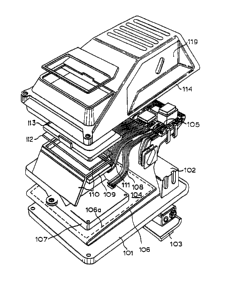
In the drawings, a case ha~ a base moulding 101 with a
planar lower face in which is formed a battery compartment 102
closed by a door 103. A flexible capacitive
electrode-carrying circuit board 104 is connected to a main
circuit board 105 and fit~ onto a concealed face of base
moulding 101. It has a reverse folded limb 106 spaced
preferably not lesg than O.S mm behind a lower capacitive
~;i~`'
~274598
sensor bearing limb thereof and preferably at a spacing of
about 2 mm that may be maintained by electrical spacer means.
The limb 106 is coated at 106a with an ink of controlled
conductivity to define the electrostatic screen means. An
inductive metal detector 107 assembly comprising a pair of
metal detector coils 130, 131 (Figure 3) on a plastics former
is connected by flexible leads 108 to the board 105. The
detector i9 intended to be a hand-held device compact enough
to go into a too~box, and for this reason it i~ important that
the metal detector assembly 107 can fit behind the board 104
rather than the two having to exist in side by side
relation~hip. A liquid crystal display 109 connected by leads
111 to board 105 i9 protected from vibration by elastomeric
mount 110 and fits behind window 112. A sliding cover 113 of
top moulding 114 protects the window 112. The sides of the
moulding 114 are indented at 119 to encourage the user to grip
the detector in a predetermined way with his fingers and thumb
in substantially the same position on each occasion of use.
This also enables a connection to be made either capacitively
or directly to the user.
Figure 2 shows the capacitive plate arrangement on a
front or lower limb of the board 104 and itq relationship to
the display 109. The electrodes on board 104 are employed in
a stray-field capacitor configuration with a transmitter plate
115 ~eparated from a linear array of nine receiver plates
116a-116i by a guard plate 117 that surrounds the plates
116a-116i and intervens between the transmitter and receiver
plates. The guard plate 117 isolates the receiver plates
116a-116i and engureg that the major part of the fiéld
reaching them has taken a circuitous path through the material
B
~274598
being sensed, increasing the depth at which a wooden stud 126
or other object concealed behind a wall 125 will significantly
influence the strength of ~ignal received at a receiver plate
by altering perceived local dielectric constant. In the
display 109 each plate 116a-116i has an as~ociated bar-type
display segment 120a-120i each consisting e.g. of 10
sub-segments in a strip which are caused to change state one
after another according to the strength of signal received at
its respective associated receiver plate 116a-116i. As the
electrodes are scanned across the wall 125 past a wooden stud
126, the presence of the stud 126 increases the current
flowing from transmitter plate 115 to receiver plates
116e-116i nearest it, resulting in a corresponding state
change in the display segment~ 120e-120i. The values in each
segment will change as the detector is scanned across a wall,
80 that the user sees the approach of the stud 126, its travel
across the electrode array 116a-116i and its departure
therefrom.
In order to provide a device of appropriately compact
dimen~ions the receiver plates 116a-116i are made as small as
poseible and in a typical embodiment they are 7.5 mm wide and
50 mm long. Further reduction of plate size results in
received signals that are too weak to handle conveniently with
the transmitter and detector circuit described below. The
transmitter plate 115 spans the ends of the plates 116a-116i
and its width is not critical and can typically be 10-50 mm
with little effect on performance. The spacing between
transmitter plate 115 and receiver plate~ 116a-116i has been
found to influence performance significantly. Spacings in the
range 10-50 mm have been evaluated and a value of 15 mm has
been found to be the optimum, with performance falling to
approximately half at values of about 7.5 mm and 30 mm. The
guard plate 117 cerves to isolate receiver plates 116a-116i
from field from transmitter plate 115 taking a path across the
~urface of board 104 which would result in a large offset
making the variation~ in received signal resulting from change
in dielectric constant of the surface under test difficult to
measure. The plate 117 is preferably not wide, and a width of
2-3 mm will normally be sufficient.
me ability to position metal detector coils 130, 131 in
material 107 behind the plates 116a-116i is important to the
production of a compact device but a capacitive sensor and an
inductive metal detector have until now been difficult to
combine in this way. The plates 116a-116i, 115 and 117 cannot
be of continuous metal otherwise operation of tranamitter coil
130 will give rise to a current flow in them that will be
sufficient to alter the field at receiver coil 131 and useful
signals from metal objects behind the test surface will be
difficult to obtain. Conductivity must, however, be sufficient
to enable the plates to act aY elements of a capacitive
sensor. We ha~e determined that the plates should be of a
material that when deposited on the substrate at the intended
thickness gives a resistance of 200-2000 ohms per square
preferably about 1000 ohms per square. Screen printable
polymer thick film inks based on graphite, for example
Mattheylec R 4000 (contains particles of graphite in an epoxy
resin), are satisfactory wherea~ silver-containing inks are
usually too conductive. The plates 115, 116a-116i and 117
likewise need to be screened from the metal detector coils and
for this purpose the back fact of board 104 is printed with
~ir~
~27~i~
one or more plates of conductive ink that provide an
electrostatic screen behind the sensor plate, such screen
plate or plates being connected to a constant ground
potential. A single electrostatic screen plate may be
satisfactory or it may be desirable to use a number of plates
defining a segmented screen in order to avoid the effects of
voltage drop.
In Figure 3, circuit board 105 is connected to the metal
detector transmitter coil 130 and receiver coil 131, to
capacitive sensor transmitter plate 115, to receiver plates
116a-116i and to guard plate 117. Other peripheral devices
include buzzer 132, mode change cwitch 301 and display 109.
The board 105 is powered from battery 134 through ON/OFF
switch 135. The principal components of the ~oard 105 are an
application-specified integrated circuit ~ASIC) ICI which is
connected to a 4-bit microcomputer IC2 which includes a
display controller for the display 109 which it works via
pin-outs 27-29, 31-62 and leads 111. The battery voltage is
~upplied from pins VMc of ICl to the input Vcc Of
microprocessor IC2 to provide power therefor, and
microproce~or pins DO, R10 and Dl provide a data clock input,
a data line and a data direction line between ICl and IC2 so
that the microcomputer IC2 may control the operation of the
ASIC ICl and receive date therefrom. A resonator Xl is
connected acros~ clock oscillator pins OSCl and OSC2 of the
microcomputer IC2 and clock pulses are also fed from the clock
oscillator to ~he uC clock pin of ICl. The plates 116a-116i
provide inputs at pins RX21 to RX29 of ICl and the guard plate
117 ig connected via lead~ 117a, 117b to ground potential
output pin ANGRND of ICl as also is the electrostatic screen
-10-
~274598
between metal detector assembly 107 and plates 115, 116a-116i
and 117 of the capacitive sensor. THE ANGRND output pin of
ICl is an internally generated analogue ground for connection
of an external decoupling capacitor between this pin and BATN.
Pulses for the tran~mitter plate 115 appear at pin TX2 of ICl
and are fed via capacitor C8 to one side of voltage set-up
transformer Tl, the other ~ide having capacitors C10, Cll
connected across it. The output voltage at pin TX2 is limited
to 3 volt~ because of working voltage requirements in ICl and
thi~ i8 stepped up by Tl to 20 voltc to give a stronger
received ~ignal at plate 116a-116i. It is difficult to obtain
a greater voltage step-up because of limitations on the
current available at pin TX2. A user connection 136 is tapped
from between C10 and Cll. The user connection come~ out to
the top moulding 114 in a region 119 thereof where the user i8
caused to place his fingers and will either be a conductive
area or will be through the ON/OFF switch. The capacitive
sensor will normally detect insulators and electrically
isolated conductors but will not detect earthed conductors
which divert the field from the transmitter plate 115 rather
than returning a stronger signal to receiver plates 116a-116i.
It i5 hoped that user connector 136 to a part of the signal to
transmitter plate 115 may avoid this happening and provide
some response of the capacitive detector from earthed
conductors.
The metal detector transmitter coil 130 is driven from
pin TXl of circuit ICl via a unity gain push-pull driver
network which act~ as a current amplifier. Pulses from pin
TXl pass via capacitor C9 and diodes D2, D3 to the bases of
tran~istor~ TRl, TR2 biased by resi3tors R9, R10, the
'~,~,,
~2~98
tran~istors having emitter resistors Rll, R12 between which an
output is fed via capacitor C13 to coil 130. The metal
detector receiver coil 131 is connected between pins RXl and
ANGRND of chip ICl via a resonant filter consisting of
inductor L1, resistor Rl and capacitor Cl.
A block schematic of the custom chip ICl is shown at
Figure 4A and 4C. Chip ICl may be divided into a signal
generator and transmitter block 201 (Fig. 4A), a receiver
circuit block 202, a pha~e sensitive detector (PSD) and analog
to digital converter (ADC) block 203 (Fig. 4B), a decoder
block 204 (Fib. 4C), a power supply 205, a buzzer driver block
206 and a test switch matrix 207. The functions of the major
blocks will be described below.
Using a 400 RHz clock signal from microcomputer IC2 the
block 201 (Fig. 4A) generates drive signals for the me~al
detector transmitter coil 130 (Pig. 3), the capacitive sensor
transmitter plate 115 (Fig. 2) and the buzzer driver 206 (Fig.
4A) and it further provides a reference signal at 210 to the
detector and converter block 203. The incoming clock signal
on line 211 passes via buffer 212 to divider 213 that
generates:
(a) eight 50 KHz square waves of relative phage 0, 45O
90....315. The square wave outputs pass to one of eight
selector 215 (Fig. 4A) controlled from decoder 204 (Fib. 4C)
by a three-bit code in control lines PHSEL 0 - PHSEL 2 so as
to pass a selected one of the phases as a reference signal in
lines 210
(b) an eight point 40KHz sine wave approximation which
is passed to filter 216 that removes residual harmonics. The
filtered sine wave is applied through buffer 220 to metal
-12-
, .....
~ c
~274~;98
detector transmitter coil 130 when control line 219 from the
decoder 204 i9 active and closes switch 217. Similarly the
sine wave is applied to capacitive sensor transmitter plate
115 via buffer 221 when control line 222 from the decoder 204
i~ active to close switch 223. ~hereby the microcomputer IC2
may selectively operate the capacitive sensor and/or the metal
detector. ~ormally control lines 219, 222 are not active
simultaneously, but a state where both lines are active i~ not
forbidden and may occur momentarily during transition between
states of switches 218, 223; and
(c) via AND gate 224 and divider 214 a 1.56 KHz square
wave buzzer drive signal is pa~sed to buzzer driver 206. Gate
224 i8 enabled when control line 225 from decoding logic 204
is active.
me 400 KHz clock signal is also passed from the output
side of buffer 212 via line 229 to the PSD and ADC block 203.
me receiver block 202 (Fig. 4A) receives the conditions
~ignals from the receiver coil 131 (Fig. 3) and from the
receiver plates 116a-116i (Pigs. 2 and 3) prior to processing
in PSD and ADC block ~03. The receiver coil 131 is connected
between pin RXll and ANGRND which define inputs to receiver
amplifier 230 of impedance about 1 megohms at 50 KHz. The
received signal may have a voltage of about 200 millivolts RMS
at 50 KHz. ~he input signal at RXll will contain a
predominant 50 KHZ signal and harmonics, but there may also be
a 50/60 Hz 3ignal present. It passes to amplifier 230 whose
gain may be set by control from the microcomputer IC2. m e
output of amplifier 230 passes to switch 231 which is closed
when line 232 from decoding logic 204 is active.
12745~B
Signals from the capacitive ~ensor receiver plates
116a_116i pa~s via inputs RX21-RX29 into the receiver block
202. The current received in each line at 50 KHZ enable~
changes in the dielectric constant of material on the
con ealed face of a wall over which the sen~or is traversed to
be determined, a change in current flowing between each
receiver plate 116a-116i ana transmitter plate 115 of about 1
nanoamp peak to peak corresponding to a change of one count at
the ADC output counter 271 of block 203. Plates 116a-116i can
pick up noise signal~ from mains cables, fluorescent tubes and
other external sources but the noise i9 effectively filtered
out by filter 245 and also at the PSD and ADC block 203 whose
re8pOn8e i8 centered on a narrow band at about 50 KHz and it3
odd harmonics. Noise in this band is expected to be
significantly less than 1 nanoamp under normal circumstances.
The capacitance being measured may typically have a value in
the range 3-40 femto farads. In a second mode drives to both
transmitter coil 130 and transmitter plate 115 are disabled
and measurement is made of a 50/60 Hz component of the input
current, the signal typically giving rise to an AC current at
that frequency of 15 nanoamps peak to peak. The lines
RX21-RX29 pas~ into an analog multiplexer 233 controlled by
four select lines 234 from the decoding logic 204, the state
of lines 234 selecting one of the nine possible input lines.
Depending upon the particular input and the selector signals
in lines 234 the sensor signal is connected to one of two
inputs or to analog ground. A fir~t output from multiplexer
233 passes to current to voltago converter 235 responsive to
signals at 50KHz and the resulting voltage is further
amplified at 236 and passes to switch 237 which is closed when
-14-
~27~ 8
control line 238 from decoding logic 204 is active, only one
of lines 232 and 238 being active at any given time. Gain of
amplifier 236 may be set by a digital code from the
microcomputer IC2. A second output from multiplexer 233 for
inputs RX24, RX25, KX26 passes to a second current to voltage
converter 240 responsive to signals at 50/60 HZ, the output
passing through bandpa~ filter 241 which passes ~ignals at
50/60 Hz. The output of filter 241 passes to peak detector
242 which provides a measure of the amplitude of the 50/60 Hz
component. The peak detector is cleared at the start of each
measurement cycle when line 243 from decoding logic 204 is
active, and a DC output at line 244 is pas~ed to PSD and ADC
block 203. ~he output of switches 231, 237 is either a signal
from the metal detector coil 131 or from the particular
receiver plate 116a-116i selected by multiplexer 233 and is
connected to bandpass filter 245 of centre frequency 50 KHz.
me output of filter 245 is amplified at a dual gain stage 246
whose gain i8 ad~usted depending on the state of line 247 from
decoding logic 204, and a received signal output is fed at
line 248 to PSD and ADC block 203.
Ihe PSD and ADC block 203 (Fig. 4B) receives a battery
voltage signal at voltage generator 265, a received signal at
line 248 from the metal detector or capacitive detector and a
line mains amplitude signal at line 244 which are respectively
passed through switches 251-253 when a selected one of lines
154-256 from decoding logic 204 is active. The output of the
three switches are fed to PSD switch 157 which is controlled
by line 158 from control logic 159 which receives the 400 KHz
clock at line 229. The output of switch 157 is fed via
resistor 258 to the inverting input of operational amplifier
--15--
1274598
259 across which capacitor 260 i connected to provide an
integrator, the non-inverting input of amplifier 259 being
connected to ground. On closure of switch 157 capacitor 260
is charged through resi~tor 258. The capacitor 260 is
discharged on closure of switch 261 when line 262 from control
logic 159 is active. When line 263 from logic 159 is active,
switch 264 closes to connect voltage generator 265 to the
input resistor 258 of to operational amplifier 259, the
voltage from generator 265 providing a reference ~ignal. ~he
output from integrator 259, 260 is fed to comparator 270 whose
output at 269 is input to control logic. 159. Control signals
pass to a ten bit counter 172 whose state can be input to
latch 272 whose state can be accessed by microcomputer ICl via
data lines 273 and decoding logic 204.
An inactive to active transition of line 275 between
decoding logic 204 (Fig. 4C) and control logic 159 (Fig. 4B)
initiates the state of a conversion cycle which is
synchronised with the line 210. At the start of the
conversion cycle over-range, under-range, start conversion,
conversion complete and ramp-up complete latches in control
logic 159 are cleared and the counter 271 is reset to zero.
me switch 261 is closed to preset the integrator capacitor
260 with a known voltage. A new conversion cycle can be
started at any time by making line 275 inactive and then
active, the control logic 159 responding to the active edge of
the signal. After the conver~ion has started, it will proceed
without intervention from the microcomputer IC2 (Fig. 4C)
e~cept where an under-range is ~ignalled at line 276, in which
case the cycle is aborted. Switches 252 and 157 are closed 30
that the voltage on line 248 charges capacitor 260 via
~274598
resistor 258 for a fixed number of cycles of the 400 KHz clock
in 229 counted at counter 271. When the ramp-up of the
voltage on capacitor 260 is complete control logic 159 clears
counter 271, opens switch 157 and closes switch 264 thereby
causing the output voltage of the integrator 259, 260 to ramp
down again, the logic 159 latching status line 280 active to
indicate at logic 204 that ramp-up is complete. ~he
microcomputer reads the status of the latch controlling line
280 and when the line i8 active is enabled to change the input
signal selection. The counter 271 is clocked by pulse~ in
line 229 during the ramp down phase of the cycle and i8
stopped by logic lS9 when the voltage on capacitor 260 falls
below the threshold of comparator 270, Vcomp. The value in
counter 271 is now loaded into latch 272 and status line 281
is set to active, allowing the microcomputer IC2 to determine
that data can be read. The output voltage reached by
integrator 259, 260 during the ramp-up phase of the cycle will
depend on the value of the voltage on input line 248. The
time for the voltage on capacitor 260 to fall to the threshold
Vcomp of comparator 270 at the controlled discharge rate of
the raDp down phase of the cycle will therefore depend on the
voltage on line 248. The digital value loaded into latch 272
will be a measure of that voltage. The operation at input
lines 244, 250 via switches 253, 251 is similar. Accordingly
the value in latch 272 can be a measure of battery voltage,
50KHz current between transmitter and receiver coils 130, 131
of the metal detector, 50KHz current between transmitter plate
115 and receiver plates 116a-116i of the capacitive sensor or
50/60 Hz current induced in plates 116d-116f by mains lines
voltage on adjacent electrical wiring. The control logic 159
., ~j
~2~45~8
sets an over-range latch and sets line 282 active at the end
of a conversion cycle if the input signal at line 244, 248 or
250 exceeds a maximum full scale input. The under-range latch
controlling the state of line 276 set to active if an
in~ufficient input voltage is obtained at line 248 to ramp the
voltage of integrator 259, 260 to the threshold of comparator
270 by the end of the ramp-up phase of the cycle, indicating
that the input signal on line 248 and the reference signal on
line 210 are out of phase and the cycle is aborted. The
microcomputer IC2 responds to an active state in line 276 by
resetting the phase of the reference signal from selector 215
via lines PHSEL 0-2 to bring thè input signal in line 248 and
the reference signal in line 210 into the correct phase so
that the PSD switch 157 is correctly timed to match an
incoming signal at line 248. At start-up, firmware in
microcomputer IC2 tests each of the phases that can be set by
output~ PHSEL0-PHSEL2 and selects the phase giving the
strongest signal. The pha~e sensitive detector and dual slope
A/D converter form a matched filter. The maximum ramp-up time
and ramp-down time are both about 2.5 milliseconds and the
maximum time between successive start conversion signals is
about 5 milliseconds allowing all 9 plates 116a-116i to be
sensed within a cycle time of 100 milliseconds together with a
50-60 Hz input status via plate~ 116d-116f, a metal detector
status and a battery status.
Ihe decoding logic 204 (Fig. 4C) provides a serial data
link between the microcomputer IC2 and the custom chip ICl,
the DATA line (D10 on Fig. 3) carrying addresses and
bidirectional data, the DCLK line carrying clock signal~ to
synchronise data transfers and the ~EAD line providing for
control of data direction.
-18-
~127L~g8
As will be apparent, the device described above performs
three major functions:
ti~ Univsrsal Object Detector for locating
inhomogeneities (e.g. studs, joists, pipes) behind
pla6terboard, chipboard, wood panels and walls and partitions
in buildings;
(ii) Metal Detector for locating metal objects behind
non-metallic surfaces;
(iii) Tracing of live cables.
These functions may be implemented in two operating
modes. A default mode of operation (at switch on) may be as a
universal object finder, where the output of the object
detector will be displayed continuously. Referring now to
Figure 2, this function is signalled by indicator zone 306 of
display 109. If the battery voltage at line 250 is below a
threshold, a low battery warning indicator 305 is activated.
If metal is detected in this mode, the microprocessor IC2 will
give the user an indication on the display in the form of a
fla~hing segment 300. The user can then, if he wishes, switch
to the second mode by pre~sing switch 201 (function signalled
by indicator 307 of display 109) which i8 a metal di~play and
mains tracing mode in which the output of the metal detector
is displayed on the display 109 as a barchart output
proportional to received signal intensity. Switching to this
second mode provides a filtering function and non-metallic
objects do not affect the display 109.
In the second mode the metal detector 130, 131 will
operate and in addition the mains tracing function of
electrodes 116d-116f will be activated by multiplexer 233. An
indication of the presence of mains will only be given if
_19--
t .
~Z74598
metal is also detected. The product should be able to
indicate the presence of live cables connected to the AC line
mains of a voltage greater ~han llOV RMS and at a frequency in
the range 40 to lOOHZ. Live cables in metal conduits or any
other form of electrical shiel~ing cannot be detected. The
cable must be live at the time that the product is used,
although it need not be carrying a current. The presence of
mains will be indicated by a flashing segment 302 on the
display and a buzzer 132 will be sounded by driver 206.
A typical detector constructed as described above may be
able to locate wooden battens behind 20 mm of plasterboard, 10
mm of plasterboard and 5 mm of plaster or 20 mm of chipboard,
and it may be able to find a 14 mm diameter copper pipe behind
10 mm of plaeterboard plu8 10 mm air gap, 10 mm of
plasterboard plu8 5 mm of plaster plus 5 mm air gap or 20 mm
of chipboard. The metal detector should be capable of finding
2.5 mm2 mains cable at 0-50 mm and 14 mm diameter copper pipe
at 0-120 mm, the location of the centre of an object at
maximum depth being to within plu~ or minus 10 mm. The
presence of mains may be detectable in a 2.5 mm2 cable
carrying 240 VRMS behind 10 mm plasterboard plus 5 mm plaster
or 5 mm plaster plus 10 mm mortar plus a plastics conduit.
It will be appreciated that the three sensor groups
operate independently and without any interaction as far as
the user i8 concerned.
It will be appreciated that modification may be made to
the embodiment described above without departing from the
invention, the scope of which is indicated in the appended
claims.
-20_