Note: Descriptions are shown in the official language in which they were submitted.
~2~49~3
BUS ARBIT~ATION CONTROLLER
Background of_the Invention
The invention relates to computer systems, and
more particularly to apparatus for arbitrating
among a plurality of asynchronous potential master
devices contending for access to a computer bus.
The proliferation of microprocessors has
produced the economic incentive and consequent
trend to construct multimicroprocessor computer
systems, where previous implementations us;ed one
high-performance processor. There is an attendant
need for a bus system through which the
microprocessors, and associated data storage
modules and peripheral devices can be
interconnected. The purpose of any bus sl:ructure
is to allow devices connected to it to transfer
data from one device to another. ~irst, however,
the device initiating a data transfer musl gain
control of the bus. Typically, control will be
delegated to any device that requests the bus to
establish a communication path between itself and
another device connected to the bus. It is
possible that two or more devices may attempt to do
this at the same time, i.e., contention may occur.
Accordingly, there must be means for deciding which
device will first access the bus. The process of
making the decision is termed arbitration, and the
process is performed by a bus arbitration unit.
A variety of devices may be interconnected by
way of a common unitary bus, the devices including
processors, data stores and peripheral devices
having various operating speeds. In a unitary-bus
system, devices other than a central processing
unit can gain control of the bus. The device in
12~91~d
control of the bus is called a "master", and those
devices with which the bus master communicates, are
termed "slaves." In a bus protocol such as the
Institute of Electrical and Electronic Engineers IEEE
896 Futurebus, each potential master is provided with bus
arbitration logic receiving bus access control
signals from the master including a unique priority
number, and inputs from control lines of the bus
indicating activity of other devices connected to
the bus including their priority numbers and bus
access request signals. The bus arbitration unit,
comprising the collective bus arbitration logic in
all potential master devices, resolves the bus
request contention and assigns the bus to a
specific device, permitting that device to become
the bus master. Data exchange transactions are
established between the bus master and a slave
device in a step-by-step manner, utilizing an
asynchronous, handshaXing process. The master (or
slave) device is not permitted to continue dialog
with another device until a reply has been received
from the slave (or master) device, the timing of
each reply being determined by the response
characteristics of the devices involved and not by
a system clock. Such an asynchronous communication
mode allows a system to be technology independent.
In a system having a bus arbitration controller
comprised of logic distributed in the modular
devices of the system, it is advantageous to imple-
ment the distributed logic inexpensively, in com-
pact microcircuits.
It is an object of the invention to provide an
improved bus arbitration controller in a
multidevice modular data processing system.
~2~4918
Another object of the invention is to provide an
improved bus arbitration controller which is distributed
among the controlled devices.
Another object of the invention is to provide new and
improved apparatus for implementing a distributed logic
bus arbitration controller characterized by inexpensive
fabrication of the arbitration units in microcircuit
packages.
Another object of the invention is to provide an
improved bus arbitration controller which synchronizes the
operation of a plurality of asynchronous devices connected
to the bus.
Still another object of the invention is to provide an
improved bus arbitration controller suitable for use with
fault-tolerant systems.
Summary of the Invention
In accordance with one aspect of the invention there
i8 provided in a computer system having a unitary bus and
at least two asynchronous devices each coupled through a
respective bus transceiver unit to the unitary bus, and an
arbitration controller distributed in the asynchronous
devices resolving contention for access to the unitary bus
by the asynchronous devices, the unitary bus having a
plurality of control signal lines including a priority
arbitration signal set ANO*-AN5*, an arbitration condition
signal AC*, and a synchronization signal set AP*, AQ* and
AR*, each of the control signal lines being common to each
of the asynchronous devices and coupled to each said
asynchronous device by wired-OR logic through the
respective bus transceiver units, the synchronization
control signal set being coupled through integrator and
threshold circuit means for preventing wired-OR glitches,
wherein the improvement comprises control logic means in
each of one of the asynchronous devices for synchronizing
the operation of the asynchronous devices by way of the
unitary bus, the control logic means receiving control
~2~4~8
signals GREQ, BRST, GMT, HIGHP and LOCK from the one
asynchronous device, the control signals AC*, AP*, AQ* and
AR* from the unitary bus respectively as control signals
AC, APF, AQF and ARF, and providing control signals GMK,
HOVR, FL and CM to the one asynchronous device, the control
logic means providing an arbitration condition signal C and
a synchronization control signal set P, Q and R each
coupled respectively through the bus transceiver unit to
the control signal lines AC*, AP*, AQ* and AR* of the
unitary bus; means in each one of the asynchronous devices
coupled to the control logic means for resolving priority
among the plurality of devices for access to the unitary
bus, the priority resolving means receiving priority
signals GA0-GA4 and the HIGHP control signal from the one
asynchronous device, the control signals AN0*-AN5* from
the unitary bus respectively as control signals AA0-AA5
and providing a control signal ZERO to the one
asynchronous device, the priority resolving means
providing a priority arbitration signal set BO0-BO5
coupled respectively through the bus transceiver unit to
the control signal lines AN0*-AN5* of the unitary bus;
means in each one of the asynchronous devices receiving a
first timing signal from the one asynchronous device and a
second timing signal ENCT from the control logic means and
providing a timing signal RP for timing the operation of
the control logic means; the control logic means comprising
combinatorial logic
/HOVR ~ (APF * /AQF * /ARF * SC * /AC)
/ENRES =
(APF * AQF * /ARF * SC * CM * /ZERO * BRST) +
(APF * /AQF * /ARF * SC * CM * AC * BRST) +
(/APF * /AQF * ARF * /SC * /CM * C * /LOCK * BRST) +
(/ENRES * ENRES-R * APF * BRST) +
(/ENRES * ENRES-R * AQF * BRST) +
(/ENRES * ENRES-R * SC * BRST) +
(/ENRES * ENRES-R * /LOCK * BRST)
~2~4~18
3b
/CM =
/BRST + ~APF * /AQF * SC * WINNER * /AC * ZERO) +
(/CM * AQF) + (/CM * ARF) + (/CM * /SC * BRST) +
(/CM * WINNER) + (/CM * AC)
~FC =
/BRST + (/APF * /AQF * ARF * SC) * (/FC * AQF) +
(/FC * AQF) + (/FC * SC) + (/FC * /AC)
/SC
/BRST + (/APF * /AQF * ARF * SC) * (/SC * APF) +
(/SC * AQF) + (/SC * ARF) + (/SC * /FC * BRST)
/FL =
/BRST + (/APF * /AQF * ARF * /SC * /AC * BRST) +
(/FL * GSET) + (/FL *HIGHP) + (/FL * LOCK)
/GMK =
/BRST + /GMT + (/GMK * GSET) + (/GMK * LOCK)
/ENCT = /FC
/ENRES-R =
/BRST + (/APF * /AQF * ARF * /SC * AC * /C) +
(/APF * /AQF * ARF * /SC * CM * C) +
(APF * /AQF * /ARF * SCl * CM * WINNER * /AC) +
(APF * /AQF * /ARF * SC * /CM * AC) +
(APF * /AQF * /ARF * SC * /CM * WINNER)
/NOCM -
/BRST + (/APF * AQF * /ARF * /FC * /ZERO) +
(APF * /NOCM) + (/AQF * /NOCM) + (ARF * /NOCM) +
(FC * /NOCM) + /ZERO * /NOCM)
~Ag~8
3c
/C = /BRST + (ARF * SC) + (/C * GREQ) + (/C * FC) +
(/C * FL) + (/C * /AQF) + (/C * /R)
/WINNER =
(/APF * /AQF * ARF * SC * EQUAL * BRST) +
(AQF * WINNER * BRST) + (AQF * /WINNER * BRST) +
(/ARF * /WINNER * BRST) + (/SC * /WINNER * BRST) +
(EQUAL * /WINNER * BRST)
/P = /BRST + (/APF * /AQF * ARF * /SC) +
(/APF * /AQF * ARF * SC */GMK) +
(/P * /FC * APF * /FL * /C) + (/P * /AQF) +
(/P * /FC * APF * GREQ * /C * /CM)
/Q = /BRST + (APF * /AQF * ARF * /SC) +
(APF * /AQF * /ARF * SC * WINNER) +
15(APF * /AQF */ARF * SC * /WINNER * /AC * GREQ) +
(/Q * /ARF) + (/Q * SC * AQF * NOMC * /CM) +
(/Q * SC * AQF * NOMC * GMK)
/R = (/APF * AQF * /ARF * /FC)
(/APF * AQF * /ARF * FC * /CM * /C) +
20(/APF * AQF * /ARF * FC * /CM * /RP) +
(/APF * AQF * /ARF * FC * /C * /RP) +
(/R * BRST * /APF)
/GSET = (/APF * /AQF * ARF */SC * C * CM) +
(APF * /AQF * /ARF * SC * WINNER * /AC):
25the priority resolving means comprising combinatorial logic
/ZERO =
(/ATEST * /AA5 * /AA4 * /AA3 * /AA2 * /AAl * /AA0) +
(/ENRES * ATEST * BO0 * BO1 * BO2 * BO3 *BO4 *
AA5 * AA4 * AA3 * AA2 * AAl * AA0)
~2~.gl8
3d
/EQUAL = ENR~S + (HIGH * AA5) + (/GA4 * AA4) +
(/GA3 * AA3 * (/GA2 * AA2) + (/GAl * AAl) +
(/GA~ * AA0)
/B00 =
ENRES + (/GA0 * /ATEST) + (HIGHP * AA5 * /ATEST) +
(/GA4 * AA4 * /ATEST) + (/GA3 * AA3 * /ATEST3 +
(/GA2 * AA2 * /ATEST) + (/GAl * AAl * /ATEST)
/BOl =
ENRES + (GAl * /ATEST) + (/HIGHP * AA5 * /ATEST) +
(/GA4 *AA4 * /ATEST) + (/GA3 * AA3 * /ATEST) +
(/GA2 * AA2 * /ATEST)
/B02 =
ENRES + (/GA2 * /ATEST) + (/HIGHP * AA5 * /ATEST) +
(/GA4 * AA4 * ~ATEST) + (/GA3 * AA3 * /ATEST)
/BO3 =
ENRES + (/GA3 * /ATEST) + (/HIGHP * AA5 * /ATEST) +
(/GA4 * AA4 * /ATEST)
/BO4 =
ENRES + (/GA4 * /ATEST) + (/HIGHP * AA5 * /ATEST)
/BO5 = ENRES + (/HIGHP * /ATEST).
The present invention provides a bus arbitration
controller which includes arbitration logic in each
potential master device connected to an IEEE 896 standard
computer bus for performing an asynchronous arbitration
protocol. Each arbitration logic unit comprises
programmable array logic circuits receiving input control
signals from the associated potential master device and
signals from all other potential master devices by way of
12749~8
3e
control lines of the bus common to all the devices, and
generates signals to resolve contention among the devices
connected to the bus and award bus mastership to the
device have priority in accordance with a predetermined
priority assignment of the devices. The arbitration logic
includes a priority resolver and control logic. The
control logic, enabled by a bus request from the associ-
ated potential master device, performs the protocol in
1~491~
concert with the other potential master devices on
the bus by using RS bistables to implement an
asynchronous state machine which, at the
appropriate time in the protocol. enables the
priority resolver and waits a predetermined time
for the resolver to settle. The resolver uses
combinatorial logic in a programmable array logic
circuit to select the highest priority potential
master device. All devices participating in the
arbitration are synchronized with one another such
that no device can start a new operation in the
procedure until all devices have completed the
present operation.
While the invention is set forth with particu-
larity in the appended claims, other objects, fea-
tures, the organization and method of operation of
the invention will become more apparent, and the
invention will best be understood by referring to
the following detailed description in conjunction
with the accompanying drawings in which:
Drawings
FIG. l is a block diagram of a multidevice
computer system having a unitary bus
PIG. 2 is a schematic block diagram of arbi-
tration logic in accordance with the instant
-nvention:
FIG. 3 is a schematic diagram of a circuit of
FIG. 2:
FIG. 4 is a schematic diagram of a
programmable array logic circuit: and
FIG. 5 is a signal timing diagram illustrating
synchronization of devices.
s ~2'7~
Description of the Preferred Embodiment
~ eferring now to the drawing for a more
detailed description of the construction, operation
and other features of the invention by characters
of reference, FIG. 1 illustrates ~ data processing
system having a central processing unit 10, a data
store module 11, a read-only store 12, and an
input/output device 13, all connected to a unitary
bus 14, which provides a com~unication path between
the various units 10-13 of the system in a manner
well known in the art. The purpose of the bus 14
is to allow devices 10-13 connected to it to
transfer data from one device to another. Fir~t,
however, one of the devices having a need to
transfer data must gain control of the bus. Any
one of the devices 10-13 can gain control of the
bus 14, and the device granted such control is
called a "master", while those devices with which
the bus master communicates, are termed "slaves." A
plurality of devices 16a, b,...n that can function
only as slaves are also connected to the bus 14.
Devices connected to the bus 14 are thus divided
into two categories, viz.: potential masters (P~s),
devices 10-13 which must gain control of the bus 14
to initiate data transfers; and the remaining
devices 16a-n, which can only act as slaves. The
potential master devices 10-13 are further divided
into two classes: (1) priority devices which
require frequent or urgent access to the bus, for
example to process real-time o?erations; and (2)
fairness devices which require less urgent access
to the bus 14.
It is possible that two or more potential-
master devices may attempt to ~ain control of the
bus 14 at the same time, i.e., contention may
6 1;~49~8
occur: therefore, there must be means for deciding
which device will be ~ranted access the bus 14.
The process of making the decision is termed
arbitration, and the process is performed by a bus
arbitration unit 20, which is not a centralized
unit, but is distributed among aIl the devices
connected to the bus 14. Each of the devices 10-
13, respectively, includes bus arbitration logic
20a, b, c,...n, which collectively form the bus
arbitration unit 20. During the arbitration
process, a priority-class device always wins access
to the bus 14 over a fairness-class device.
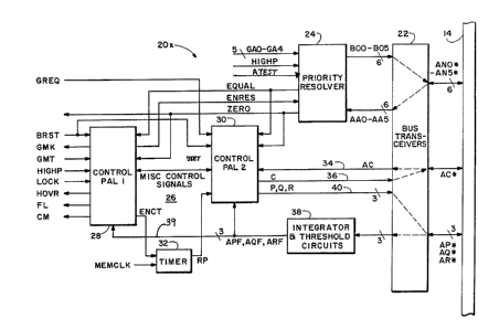
Referring to FIG. 2, representative bus
arbitration logic 20x is shown in greater detail.
Each device which is connected to the bus 14, and is
a potential master, includes bus arbitration logic
as shown in FIG. 2. The circuits depicted in FIG.
2 compete with like circuits in all other devices
to deter0ine which device will acquire access to
the bus 14 as a bus master. The following
discussion of the bus arbitration logic 20x applies
generally to logic in each device connected to the
bus 14; however, to differentiate between the
particular device illustrated, and other devices
having similar bus arbitration logic, the
illustrated device is referred to as the "instant"
device. All PM devices participate in every
arbitration operation, even though a particular
device may not require immediate access to the bus
14. The arbitration process $s asynchronous
wherein each PM device participates in a state
machine that is distributed throughout all the PM
devices on the bus 14. The distributed
configuration ensures that each transition from
3S state-to-state is agreed upon by each individual
7 12~ 4 91 8
potential-~aster device.
The bus 14 interface signal leads utilize
negative logic, i.e., a less-positive level on the
signal lead of the bus 14 represents a logic 1.
S The voltagè level of each such lead repre~ents the
OR function of the signals applied to it by the
various PM devices connected to the bus. In
accordance with standard practice, the logic-signal
names of the bus leads are designated with an
asterisk (*) to indicate that binary 1 is
represented by the less-positive level. Logic
levels of the signals of the bus arbitration logic
are conventional positive logic.
Each of a plurality of interface signal leads
AN0*-ANS~, AC*, AP*, AQ*, AR* of the bus 14 is
connected to each PM device along the bus through
a bus transceiver 22 in a well-known open-
collector output arrangement, wherein each lead
carries a signal representing the OR function of
the signals applied to the lead by the various PM
devices. ~he AN0*-ANS* signals represent an
arbitration number. Each competing device on the
bus 14 asserts an internally generated,
predetermined arbitration number on the AN0*-ANS*
signal leads, and when the arbitration cycle ends,
the highest priority arbitration number remains on
the leads. The ANS* signal, which indicates if a
device is in the priority or fairness class, is
enabled by priority-class device~ in response to a
HIGHP signal asserted by the device, and disabled
by fairness-class devices.
The bus arbitration logic 20x comprise3 a
priority resolver 24, and control logic 26
including first and second programmable array logic
(PAL) circuits 28, 30, and a timer circuit 32. The
8 127Ag~8
ti~er circuit 32 comprises a four-bit counter
receiving a timing signal MEMCLK generated by the
device, and a control signal ENCT which enables the
counter. After counting a predetermined number of
the MEMCLK pulse~, the timer circuit 32 generates a
control signal RP indicating to the control logic
26 an end of an arbitration delay time or period.
The priority resolver 24 receives a signal set GA0-
GA4, representing a predetermined arbitration
number unique to the particular device in which the
bus arbitration logic 20x resides. The arbitration
number determines a device's priority within the
arbitration class. The HIGHP signal designates the
device as a priority class device, and when high,
enables the priority arbitration mode in the
resolver 24.
The AC* (arbitration condition) signal lead of
the bus 14 is as~erted by a device to signal other
devices on the bus 14 that bus access is needed by
the device. An AC* signal received by the bus arbi-
tration logic 20x is regenerated in the bus trans-
ceivers 22 as an AC signal and applied via lead 34 to
the control logic 26. Devices requiring bus 14
access generate, in the control logic 26, a signal,
C, on lead 36, which is applied to the driver of
the bus transceiver 22 corresponding with the AC*
lead of the bu~ 14. The AC* interface lead serves
a dual purpose: during arbitration the line serves
as a general condition or status line indicating
the existence of an error condition if enabled
when no arbitration procedure is in progress the
AC* line is used for signaling a bus request.
The AP*, AQ*, and AR* interface leads of the
bus 14 are coupled by way of integrator and
threshold circuits 38 to the PALs 28, 30 of the
12t749~8
control logic 26, respectively, as signals APF, AQF, and
ARF on a ~us 39. The AP*, AQ*, and AR* signals, which
comprise a synchroni7ation si~nal set, are used to define
a distributed state machine among the devices on the bus
14 participating in arbitration, and indicate a state of
the operation which is currently valid, thereby performing
a handshake operation among the asynchronous devices and
maintaining synchroni~ation of the devices during the
arbitration process. Corresponding device signals P, Q,
and R are asserted by the PAL 30 and coupled by way of bus
40 and bus transceivers 22, respectively, to the AP*, AQ*,
and AR* interface lèads under control of logic 26.
The integrator and threshold circuits 38 solve
a problem that occurs in wired-OR lines. If two or
more devices are holding a bus line at binary 1,
and one of the lines switches to binary 0, the
redistribution of current in the line can cause a
spurious pulse to appear on the line. This pulse,
popularly known as a wired-OR glitch, can cause
devices to misinterpret the state of the line as
representing 0, although other devices are still
applying 1. The effect of wired-OR glitches i3
overcome by including, in each line, an integrator
and threshold circuit designed so that the longest
possible glitch or series of glitches will not
cause the output to switch erroneously. Referring
to FIG. 3, a representative one of the integrator
and threshold circuitQ 38 is shown on the AR~ bu~
line comprising a resistor 42 connected to a bus
receiver 44 of the bus transceivers 22, the bus
receiver 44 having an input connected to the AR~
bus line. A capacitor 46 to ground and the
resistor 42 form an integrator circuit in the AR~
line. A diode 48 provides a path for recharging
lo ~2~4918
the capacitor 46. The diode/resistor/capacitor
48/42/46 network filters pul~e~ having widths of 25
nanoseconds or less, which in the presently
described embodiment of the invention, is less than
twice the propagation delay of the bus. An
inverter 50 serves as a logic-level regenerating
circuit which prevents regeneration of the spurious
pulse-~ as a change in logic level; the AR* signal
is regenerated as the ARF signal on the bus 39.
The inverter 50 functions as a threshold circuit
which provides a consistent and extremely tight
threshold voltage (1.55 + 0.05 volts in the present
embodiment) to reject anomalous logic levels
generated by the filter in response to spurious
pulses on the AR* line. For additional information
~regarding the phenomenon of wired-OR glitches, see
D. B. Gustavson and J. Theus, "Wire-OR Logic on
~ransmission Lines," IEEE Micro, Vol.3, No. 3, June
1983, pp. Sl-55.
Input signal~ to the control logic 26 are
named and a brief description of the function of
each signal is listed as follows:
GREQ -Bus Request signal - This signal,
asserted by the device, i~ enabled to
request bus ~aster~hip for the device.
BRST -Board Reset - Resets control bistables of
the control logic 26.
GMT -Bus Mastership Terminate/Done. Asserted
by the instant device, this signal, when
enabled, indicates that the instant
device will release mastership of the bus.
HIGHP -High Priority - Enabled by the instant
device, this signal, when enabled,
enables the priority arbitration mode.
4g~
LOCK -A current master device asserts this
signal to force an arbitration cycle with
a zero arbitration number for the purpose
of cancelling locking operations in slave
devices.
MEMCL~ -Me~ory Clock - Clock signal input from
the instant device to the timer 32 for
timing the operation of the priority
resolver 24.
The control logic 26 comprises a plurality of
RS bistable logic elements connected to perform a
process or protocol of arbitration and conl:rol
acquisition of a device connected to a unil:ary bus
shared and in contention with other devices on the
bus. The control logic 26 is implemented in the
PALs 28, 30 which function together as a single
controller. Output and internal signals labeled
MISC CONTROL SIGNALS on the bus 29 between the PALs
28, 30 are listed and defined as follows. A double
asterisk (**) adjacent the signal indicates the
signal is also an output signal to the device(s):
PAL 28 to PAL 30
GM~ ** -Bus Acknowledge or Grant Signal - When
enabled, the instant device has mastership
of the bus 14.
CM ** -Current Master - When enabled, this signal
indicates that the instant device is the
current master of the arbitration process.
FL ** -Fairness Lock - When enabled, this signal
indicates that the instant device must wait
for a fairness release cycle before it can
make another bus request.
FC -First Cycle - When enabled, this signal
12 127 4g ~8
indicates that the first half of the six-
state arbitration process is in progress
(operation numbers 1, 2 and 3).
SC -Second Cycle - When enabled, this signal
indicates that the second half of the six-
state arbitration process is in progress
(operation numbers 4, 5 and 6~.
PAL 30 to PAL 28
GSET -Grant Set - When enabled, this signal sets
or enables the GMK bus grant signal.
ENRES-R -Enable Resolver Reset - When enabled, this
signal disables the E~RES enable resolver
signal.
5 WINNER -This signal enabled indicates that the
instant device is the winner of the
priority competition.
C *~ -This slgnal is sent to the bus tran~ceivers
by the PAL 30 as the C signal to be
regenerated as the AC* b~s signal.
PAL 30
NOCM -This signal is used internally in the PAL
30 and signals that there is no current
master on the bus 14.
At an appropriate time in the protocol, the
control logic 26 enables the priority resolver 24,
and responsive to the timer circuit 32, waits a
predetermined time for the resolver 24 to settle.
The priority resolver 24, a PAL, incorporates a
combinatorial logic circuit, i.e., one having no
feedback paths, so that the number on the
arbitration lines ANO*-A~5* depends only on the
signals currently being applied, and not on any
13 ~27~91~
past history, to determine which devi~e has the
highest arbitration number. The priority resolver
24 has the the following input ~ignals:
AAO-AA5 -The ANO*-AN5* bus signals regenerated by
the bus transceiver~ 22.
GAO-GA4 -The predetermined arbitration number of
the instant device.
ENRES -Enable Resolver - ~len asserted by the
control logic 26, this signal enables the
resolver output signals BOO-B05 to the
bus 14 via the bus transceivers 22.
ATEST -Arbitration Test - Enables diagnostic
testing of the resolver 24 circuits.
The input signals of the arbitration resolver
24 are decoded into output signals in accordance
with equations programmed into the PAL. The logic
structure of the output signal~ i8 disclosed below
in the form of Boolean logic equations. In the
equations, a "+" symbol denotes an OR function, and
a "*" symbol indicates an AND function. A "/"
symbol prefix of a logic name means that the signal
i8 the complement of the named signal (positive
logic i~ utilized), i.e., "/" means that the
voltage level associated with the term is the less
positive level, and the term is enabled or high
when that level i8 present on the signal node. For
example, the ZERO signal is enabled when the /ZERO
signal node i8 at the less-positive level, and
disabled when the /ZERO node i8 at the more
positive level. A logic term without a suffix
symbol indicates that the voltage level associated
with the term is the more positive level and the
term is enabled or high when that level is present
127A9~8
14
on the signal node. The logic terms correspond
with the logic signal names utilized throughout the
present specification: lower case characters are
not used in the logic terms.
/ZERO = (/ATEST * /AA5 * /AA4 * /AA3 * /AA2 * /AAl * /AAO)
+ (/ENRES * ATEST * BOO * BOl * B02 * B03 * B04
* AA5 * AA4 * AA3 * AA2 * AAl * AAO)
/EQUAL = ENRES + (HIGHP * AA5) + (/GA4 * AA4)
+ (/GA3 * AA3) + (/GA2 * AA2) + (/GAl * AAl)
+ (/GAO * AAO)
/BOO = ENRES + (/GAO * /ATEST) + (HIGHP * AA5 * /ATEST)
+ (/GA4 * AA4 * /ATEST) + (/GA3 * AA3 ~ /ATEST)
+ (/GA2 * AA2 * /ATEST) + (/GAl * AAl * /ATEST)
/BOl - ENRES + (GAl * /ATEST) + (/HIGHP ~ AA5 * /ATEST)
I (/GA4 * AA4 * /ATEST) + (/GA3 * AA3 * /ATEST)
+ (/GA2 * AA2 * /ATEST)
/R02 o ENRES + (/GA2 * /ATEST) + (/HIGHP * AA5 * /ATEST)
+ (/GA4 * AA4 * /ATEST) + (/GA3 * AA3 * /ATEST)
/B03 o ENRES + (/GA3 * /ATEST) + (H~GHP * AA5 * /ATEST)
+ (/GA4 * AA4 * /ATEST)
/B04 ~ ENRES + (/GA4 * /ATEST) + (/HIGHP ~ AA5 * /ATEST)
/B05 = ENRES + (/HIGHP * /ATEST)
For the purpose of the ensuing discussion
describing tbe contention resolution phase of an
arbitration cycle, a lower case signal na~e denotes
a signal sent by the device to the bus transceiver
15 ~ 749~8
circuits 22 and onto the bus 14; an upper case
signal name denotes the si~nal as received by the
device from the bus transceiver circuits, and reflects
what actually occurs due to the wired-OR
configuration of the bus 14. This convention
eliminates the confusion attendant the change of
signal names that occurs, for example, at the bus
transceivers 22, where the AN*(n) signals input to
the resolver bec~me the AA(n) signals and the BO(n)
output signals from the resolver become the AN*(n)
signals on the bus 14.
The wired-OR configuration of the bus allows
the competing devices to determine which of them
ha~ the highest arbitration number. When the
arbitration control logic 26 sigr.als for
competition (ENRES enabled), each device places its
unique arbitration number on the ANO*-A~4~ lines of
the bus. After this instant, if any digit an(n)
ha~ a value O while the digit AN(n) on the
corresponding bus line is 1, then all the digits of
lower significance, an(n-l) to anO, are disabled by
the priority resolver 24. After a time delay Tarb
for the system to settle, the device winning the
competition will still be asserting its AN* lines
and losing devices will have disabled one or more
of their A~* lines.
When the arbitration process settles out in
the resolver 24 with the instant device as the
arbitration winner, the resolver 24 enables the
EQUAL signal that is coupled to the control logic
26, indicating that the arbitration number of the
present device is asserted on the ANO*-AN5* lines
of the bus 14. When the AAO-AA4 signals are
disabled, the resolver 24 enables the ZERO signal
which is coupled to the control logic as an
16 ~2 7 4 9~ 8
indication that the arbitration number on the bus
14 is zero. The BOO-BO5 (an(n)) output signals of
the resolver 24 are inverted in the bus
transceivers 22 and regenerated on the bus 14 as
the ANo*-AN5 signals.
Control Synchronization
The control synchronization process which syn-
chronizes the operation of the as~nchronous devices
connected to the bus 14 is performed collectively by
the control logic 26 in each of the devices, imple-
mented as PALs 28, 30. The PALs 28, 30 are disclosed
below in the form of Boolean logic equations uti-
lizing the same conventions as previously described
with reference to the priority resolver 24 PAL.
First PAL 28
/HOVR - (APF * /AQF * /ARF * SC * /AC)
/ENRES = ~APF * AQF * /ARF * SC * CM * /ZERO * 3RST)
+ (APF * /AQF * /ARF * SC * CM * AC * BRST)
+ (/APF * /AQF * ARF * /SC * /CM * C * /LOCK * BRST)
+ (/ENRES * ENRES-R * APF * BRST)
+ ~/ENRES * ENRES-R * AQF * BRST)
+ ~/ENRES * ENRES-R * SC * BRST)
+ ~ENRES * ENRES-R * /LOCK * BRST)
/CM ~ /BRST + ~APF * /AQF * SC * WINNER * /AC * ZERO)
+ (/CM * AQF) + (/CM * ARF) + (/CM * /SC * BRST)
+ ~/CM * WINNER) + (/CM * AC)
/FC /BRST + (/APF * /AQF * ARF * SC) + (/FC * AQF)
+ (/FC * AQF) + (/FC * SC) + (/FC * /AC)
/SC - /BRST + (/APF * /AQF * ARF * SC) + (/SC * APF)
17 i2~49~8
+ (/SC ~ /AQF) + (/SC * ARF) + (/SC * /FC * BRST)
/FL = /BRST + (/APF ~ /AQF ~ ARF * /SC * /AC * BRST)
+ (/F~ * GSET) + (/FL ~ HIGHP) + (/FL * LOCK)
/G~K = /BRST + /GMT + ~/GMK * GSET) + (/GM;g * LOCK)
/ENCT = /FC
Second PAL 30
/ENRES-R = /BRSr + (/APF * /AQF * ARF * /SC * AC * /C)
+ (/APF * /AQF * ARF * /SC * CM * C)
+ (APP * /AQF * /ARF * SCl* CM * WIN~ER * /AC)
~ (APF * /AQF ~ /ARF * SC * /CM * AC)
+ (APF * /AQF * /ARF * SC * /CM * WI~NER
/NOCM = /BRST + (/APF * AQF * /ARF * /FC * /ZERO)
+ ~APF ~ /NOCM) + (/AQF * /NOCM) + (ARF ~ /NOCM)
+ (FC * /NOCM) + /ZERO * /NOCM)
/C - /BRST + (ARF * SC) + (/C * GREQ) + (/C * FC)
+ (/C * FL) + (/C * /AQF) + (/C * /R)
/WINNER s (/APF * /AOF * ARF * SC * EQUAL * BRST)
+ (AQF * WINNER * BRST) + (AQF * /WINNER * BRST)
+ (/ARF * /WINNER * BRST) + (/SC * /WINNER * BRST)
+ (EQUAL * /WINNER * BRST)
/P ~ /BRST + ~/APF ~ /AQF * ARF * /SC)
+ (/APF * /AQF * ARF * SC * /GMK)
+ (/P * /FC * APF * /FL * /C) + (/P * /AQF)
+ (/P * /FC * APF * GREQ * /C * /CM)
/Q = /BRST + (APF * /AQF * /ARF * /SC)
+ ~APF * /AQF * /ARF * SC * WINNER)
18 ~2~9~1S
+ (APF * /A(2F * /ARF * SC * /WIN~ER ~ /AC * GREQ)
+ (/Q * /ARE`) + (/Q * SC * AQF * NOMC * /CM)
~ ( /Q * SC * AQF * NOMC ~ GMK)
/R ~ ( /APF * AQF * /ARF * /FC ~
+ ( /APF * AQF * /ARF * FC * /CM * /C)
+ ( /APF * AQF * /ARF * FC * /CM * /RP )
+ ( /APF * AQF * /P.RF ~ FC * /C * /RP )
+ ( /R * BRST ~ /APF )
/GSET = ( /APF * /AQF * ARF * /S~' ~ C * CM)
+ ( APF t /AQF * /ARF * SC * WINNER * /AC )
In the present invention, the PALs 24, 30, and
32 are Model 20L8A programmable array logic cir-
cuits manufactured by Monolithic ~emories Inc.
Referring to FIG. 4, a PAL circuit iS illustrated
in part, comprising an OR gatel;0 provided with a
number of inputs by way of drivers 62 from horizon-
tal conductors of a matrix 64, with the OR gate 60
driving a tri-state amplifier-inverter 66. An
output 68 of the amplifier-inverter 66 is coupled
through an amplifier 70 to provide both feedback
and inverted feedback signals to vertical conduc-
tors of the matrix 64. The amplifier-inverter 66
may be tri-stated (opened) by an enabling input 72.
The array depicted in FIG. 4 i3 repeated for each
desired output signal on successive output leads
such as the lead 68. The vertical lines of the
matrix 64 represent conductors crossing over but
not connected to the horizontal conductors, and
carry input signals from successive input ampli-
fieræ such as amplifier 74 as well as feedback
signals from successive feedback amplifiers such as
the amplifier 70. To implement the logic previous- .
ly disclosed as Boolean expressions in the PAL,
19 ~2'7491~3
connections are enabled at appropriate crossovers
of the horizontal and vertical conductors.
Referring now to FIG. 5, the first four
operations of the rontrol synchroni~ation process
among three devices DA, DB, and DC are shown. Each
device participating in the handshake operation
controls its own variable signals P, Q, and R.
The signals on the AP*, AQ* and AR* bus lines
are used to form a distributed state machine a~ong
the devices participating in arbitration. Initial-
ly, the P, Q, and R signals in every device are set
to the values 0, 0, 1 respectively. Device A (DA)
starts the sequence of operations by enabling the
variable P, causing the bus line AP* to be enabled
(less positive level). DA concurrently starts a
first operation, as indicated in FIG. 5 by the
designation -Al-, device A performing operation
number 1. The remaining devices DB and DC sense
the AP* bus line enabled, and respond by enabling
their respective P signals and starting their own
first operations Bl, Cl. When each device com-
pletes the first operation, the respective R sig-
nals in each device are disabled, and only when the
slowest device, in this instance DC, has disabled
it~ R signal, does the AR* bus line switch to zero
(~ore positive level)~ All devices DA, DB, and DC
respond to the AR* line changing state by enabling
signal Q and starting a second operation, respec-
tively A2, B2, C2. As each device completes the
second operation, the signal P is disabled, and
when the slowest device, in this instance DC, dis-
ables its P signal, the AP* bus line switches to 0.
All devices, DA, DB, and DC respond to the AP*
signal changing state by enabling the Q signal and
starting a third operation, re9pectively A3, B3t
20 12749i8
and C3. When each device completes the third
operation, the respective Q signal is disabled, and
only when the slowest device, in this instance DA,
has disabled its Q signal, does the AQ~ line switch
to zero. If a fourth operation is called for by
enabling the SC signal (second cycle), then all
devices respond to the AQ* line changing state by
enabling the P signal once again and starting a
fourth operation. Operations 4, 5, and 6 are syn-
chronized similarly as described above with
reference to operation numbers 1, 2, and 3.
Control Procedures
-
Any PM device connected to the bus 14 may
initiate an arbitration procedure to access the bus
or to acquire release from the fairness restriction
by enabling the bu~ request signal GREQ. Prior to
beginning an arbitration procedure, a device having
a requirement for bus arbitration enables the C
~ignal on the lead 36 in response to the GREQ
signal; however, if the device is inhibited by the
fairness restriction, the C signal i8 inhibited.
All other devices disable the C signal. An
arbitration procedure comprises a series of
numbered operations or states, listed below, that
are started and completed as described above with
reference to the control synchronization process.
Operation 1
All devices lock the variable C signal at the
current value, and detect whether or not a current
master has control of the bus. The absence of a
current master is indicated during operation 1 by
enabling the NOCM signal in response to the AN0*-
AN4* bus lines being disabled (signal ZERO enabled).
21 ~2~18
Operation 2
All devices evaluate the AC* line. If the AC*line is disabled, all devices register that a
fairness release procedure has been initiated (C
signal disabled) and that the procedure shall
terminate at the end of operation number 3.
Devices inhibited from making bus requests under
the fairness restriction disable the restriction at
the end of operation 3 by disabling the FL signal;
such devices can then enable bus requests after
operation 3 is completed.
If the AC* line is enabled, then all devices
register that the procedure is a call for
arbitration, and that the procedure shall terminate
at the end of operation number 6. All competing
devices activate the AN* lines with their
respective arbitration numbers, and enable the
contention resolution logic as previously described
with reference to Fig. 2. If a device which is the
current master is not competing for the bus, the
non-competing device removes its arbitration number
from the AN* lines. The current master and all
competing devices each begin timing the interval
Tarb in accordance with their own logic circuits,
wherein
Tarb = 2 * TpRT + TsMax + 7 * Max~Td, Tek(0 c= k ~= 4), Tf]
and where
-Ts is the delay introduced by the AR* line
integrator of the integrator and threshold
circuits 38;
-Td is the time from the integrator output
switching to 0, and the activation of the
22 ~ gl 8
AN5* line:
-Tek(0 <= k <= 4) is the time from an
externally produced change on bus line
AN(kll)*, and the resulting change on line
AN(~
-Tf is the time from an externally produced
change on bus lines ANO*-AN4* to the
resulting change on the line indicating a
l~in or loss of the arbitration cycle;
-TsMax is the maximum value of Ts;
-~ax[ ] is the largest value among Td, all the
'rek, and Tf in the device logic: and
-TpRT is the round trip bus propagation delay,
Erom one end of the unitary bus 14 to the
other end of the bus, and return.
Operation 3
No new action is initiated during this
operation other than moving to the next operation.
The fairness procedure concludes with this
operation.
Operation 4
Each device that initiated timing Tarb in
operation 2 waits in thi3 state until Tarb times
out. Prior to the start of operation 5, if a
device has error detection logic, then the device
carries out the error checks, and any device
detecting an error enables the C signal. Devices
not detecting an error, and devices without error
detection logic, disable the C signal. A priority
device with a higher arbitration number than the
value on the AN* lines enables the C signal if it
wishes to force a rearbitration cycle. Devices can
record the identity of the next bus ~aster by
23 12~918
storing the contents of the AN~ lines. When there
is no current master as determined in operation 2,
then the all the devices participating in
arbitration initiate operation 5. If a current
master device exists, then that device initiates
operation 5 when it is ready t~ release the bus to
another master device.
Operation ~
All devices complete the ~rocedures started
above; all devices lock their variable C signal
(rearbitrate) at its current value.
Operation ~
All devices evaluate the ~us line AC*. If the
AC* line ls O, then all devices, in response to the
HOVR handover signal enabled, cancel any interlocks
loft by the parallel protocol, and the mastership
of the bus transfers from the current master to the
PM device having the arbitration number which
appeared on the AN* lines duri~g operation 5. One
example of such an interlock is one imposed by a
first central processing unit on a second central
processing unit when both are performing read-
25 modify-write operations on a com~on data store
segment. Devices losing the arbitration
competition remove their arbitration number from
the AN* lines.
If the AC* line is 1, then the current master
30 places its arbitration number on the AN* lines and
all other devices remove their arbitration numbers.
The bus arbitration controller of the present
invention thus uses programmable logic array circuits
to implement distributed arbitration logic in
35 inexpensively fabricated microcircuit packages. The
~274g~8
24
controller synchronizes the operation of a plurality
of asynchronous potential master devices contending
for access to the bus and awards the bus to the
requesting device having the highest priority
S arbitration number.
While the principles of the invention have now
been made clear in the foregoing illustrative
embodiment, there will be immediately obvious to
those skilled in the art many modifications of
structure, arrangement, proportions, the elements,
material and components used in the practice of the
invention, and otherwise, which are particularly
adapted for specific environments and operating
requirements without departing from those
principles. The appended claims are, therefore,
intended to cover and embrace any such
modifications, within the limits only of the true
spirit and scope of the invention.