Note: Descriptions are shown in the official language in which they were submitted.
~Js
- 1 - RD 16,820
POLYCRYSTALLINE DI~MOND AND CB~ CUTTING TOOLS
This invention relates to the production of
polycrystalline diamond and cubic boron nitride (CBN)
cutting tools.
Canadian Application Serial No. 529,177,
filed February 6, 1987, now Canadian Patent
1,254,451, for POLYCRYSTALLINE DIAMOND AND CBN
CUTTING TOOLS by R. Komanduri, assigned to the
assignee hereof, discloses a cutting tool comprised
of a polycrystalline layer of diamond or cubic boron
nitride which has a cutting edge and at least one
straight edge wherein one face of the polycrystalline
layer is adhered to a substrate of cemented carbide
and wherein a straight edge is adhered to one side of
a wall of cemented carbide which is integral with the
substrate, the thickness of the polycrystalline layer
and ths height of the wall being substantially
equivalent.
Canadian Application Serial No. 529,644,
20 filed February 13, 1987, for POLYCRYSTALLINE DIAMOND
AND CBN CUTTING TOOLS by R. Komanduri, assigned to
the assignee hereof, discloses a cutting tool
comprised of a polycrystalline layer of diamond or
cubic boron nitride adhered to a peripheral recessed
round portion of a cemented carbide substrate
structure, one face of the layer being adhered to the
bottom surface of the recessed portion and an inner
~7~7~
RD 16,820
-- 2
round side of the layer being adhered to the wall of
the recessed portion, said layer having a round
cutting edge and a thickness equivalent to the height
of the wall.
Polycrystalline diamond and cubic boron
nitride cutting tools have a thin diamond/CBN layer
(about 0.030 inch) on top of a cemented tungsten
carbide substrate. Because of the high
temperature-high pressure process and high processing
costs involved in the fabrication of ultrahard tool
materials the cost of these tools is very high. With
the intrcduction of new, less e~pensive ceramic tools,
comretitioll is oecor!ing intense bet-~en tr.e superhaLd
tools and ceramics. One way to reduce the cost of the
tools is to reduce the material costs by providing
small size inserts. The final size can be obtained by
pressing to near-net size or pressing a larger size
insert and slicing it into small segments. This
invention deals with the latter case.
Another way to reduce the costs is to reduce
the fabricating costs. The raw material (diamond or
CBN) cost is minimized by this invention by using it
only in the region where it is needed for the cutting
operation. This will, at the same time, reduce the
fabrication costs, since most of the tool to be
fabricated involves cemented carbide material instaed
of the hard, super abrasive diamond or csN. Cost of
the insert can be further reduced by slicing of the
specimen into four tools by wire electrical discharge
machining (EDM) by this invention. The cemented
carbide backing at the bottom and on the side of the
resulting cutting tool provides the support base
required for the relatively brittle polycrystalline
diamond/CBN layer. It also facilitates brazing of the
tool to the tool holder without degrading the
diamond/CBN layer.
7~
RD 16,820
-- 3
This invention will be bett.er understood
from the following description and drawings in whieh:
FIGURE 1 is a top view of one embodiment of
the present composite useful for slicing into a
5 plurality of cutting tools;
FIGURE 2 is a eross seetion of the eomposite
of Figure 1 taken on line 2-2;
? FIGURE 3 is a view in perspeetive of a
eutting tool formed by eutting through the composite
10 of Figure 1 on line 3-3;
FIGURE 4 is a top view of another embodiment
of the present composite useful for slicing into a
- ~iuc~.iity of _~tting too1s; and
~IGURE 5 is a view in perspective of a
15 eutting tool produeed by eross-seetionally slieing the
eomposite of Figure 4 along line 5-5 or 5'-5'.
- Briefly stated, the present proeess for
producing a composite comprised of a circular
polycrystalline diamond or cubic boron nitride layer
20 adhered in the recess of a cemented earbide substrate
strueture eomprises forming a substrate strueture
eomprised of a substrate with a disk-shaped reeess
wherein said reeess is substantially eentrally
disposed in a faee of said substrate, said eemented
25 earbide being eomprised of polyerystalline metal
earbide containing a metallic eementing agent, filling
said reeess with crystals of diamond, heating the
resultinq assembly under an applied pressure to a
temperature above the melting point of said metallic
30 cementing agent but below a temperature which has any
signifieant deleterious effeet on said assembly for a
period of time suffieient to form said composite and
recovering said composite, the thickness of said
polycrystalline diamond layer being substantially
35 equivalent to the depth of said reeess.
~ The structure and size of the present
5 :ZL~75
RD 16,820
_ ~ _
composite allows it to be cross-sectionally sliced to
form a plurality of cutting tools.
In the present process a substrate structure
comprised of polycrystalline metal carbide containing
a metallic cementing agent, i.e. a cemented carbide,
is used. Cemented carbide bodies are commercially
available and are well known in the art, and have been
used as substrates for polycrystalline diamond/CBN
cutting tools.
Generally, the cemented carbide body is
produced by forming a compact of a sinterable carbide
moldil!g powder into a desired shape and ~size and
~intering th.e compac~. Usual~y, the sinterable pow~er
is comprised of a mixture of a metal carbide powder
and powdered metallic cementing agent, preferably
selected frorn the group consisting of cobalt, nickel
or iron. The carbide portion of the molding powder is
preferably selected from the group consisting of
tungsten carbide, titanium carbide, tantalum carbide,
and mixtures thereof (although other carbides may be
added to obtain special properties). The compact is
sintered in a protective atmosphere such as nitrogen
or argon at a temperature which depends largely on its
composition for a period of time sufficient to produce
a cemented carbide of desired density. Suitable
sintering temperatures generally range from
about 1340C to 1600C. Generally, the composition of
the compact as well as the resulting sintered body is
comprised of from about 75 to 97% by weight carbide
and about 3 to 25% by weight of the metallic cementing
agent.
Preferably, the cemented carbide of the
present invention has a porosity of less than
about 15% by volume, more preferably less than
about 10%, still more preferably less than about 5%,
still more preferably less than about 1~ by volum~e,
and most preferably it has no significant porosity.
5~75
RD 16,820
-- 5
In carrying out the present process, a
substrate structure is formed which is comprised of a
substrate with a disk-shaped recess centrally or
substantially centrally disposed in one face of the
substrate. Generally, the substrate structure is a
flat piece with its upper or top surface containing
the disk-shaped recess. Preferably, the unsintered
compact is in the form required of the present
substrate structure and sintered to produce the
present substrate structure directly. Alternatively,
the present substrate structure can be produced by
forming tle disk-shaped recess in the sintered
subs.ra~e by a techlljque su~h as, for example,
electrical discnarge machining. The substrate can
have any of a number of desired shapes such as, for
example, that of a cylinder or a square. The diameter
of the cemented carbide substrate in the composite can
vary depending largly on the particular cutting tools
to be formed, but generally it ranges from about .05
inch to about 1.5 inch.
The substrate should be at least
sufficiently thick so that it can be held in a cutting
tool holder. Generally, the thickness of the
substrate, except for its recess portion, is at least
about 0.04 inch, and frequently it ranges from
about 0.04 inch to about 0.25 inch.
In one embodiment, the recess of the
substrate structure is provided with a four-sided
elongated cemented carbide element centrally or
substantially centrally disposed therein. Each side
of the element is in the form of a cutting tool nose
of given radius and usually all four sides are
equivalent or substantially equivalent. The element
is useful for forming in situ four cutting tool noses
of substantially corresponding radii in the central
portion of the polycrystalline diamond or cubic boron
~.~7S~75
RD 16,820
-- 6
nitride layer. Specifically, the central portion oE
the polycrystalline layer is formed in contact with
the sides of the element. The height of the element
should be equivalent or substantially equivalent to
the thickness of the polycrystalline layer to be
formed. At this point in the process, the element may
or may not be integrally bonded to the bottom surface
of the recess. If not bonded, integral bonding of the
cemented carbide element to the bottom surface of the
recess is effected during the present process. If
desired, the element can be formed in situ by
initially ,orming the unsintered compact into the form
c,f ~he substra~e ~rLucture ~ith the unsintered elernent
integrally extending from the bottom surface of the
recess and sintering such structure. Alternatively,
the element can be preformed in the sintered substrate
by a technique such as electrical discharge
machining. The element reduces the amount of crystals
required to form the cutting tools and is especially
useful for larger sized tools.
Since the substrate structure is comprised
of cemented carbide, its dimensions are not
significantly changed by the present process, i.e. it
substantially retains its shape. In the final
product, i.e. composite, the thickness of the
polycrystalline diamond or cubic boron nitride layer
is equivalent or substantially equivalent to the depth
of the recess.
The recess of the cemented carbide substrate
structuxe is filled with crystals of diamond or cubic
boron nitride. The thickness of the filling depends
largely upon the thickness and type of polycrystalline
layer desired in the final product and is determinable
empirically. Preferably, the crystals fill the recess
in excess of its depth to produce a higher degree of
consolidation under the present high pressure
RD 16,820
-- 7
conditions. The average size of the crystals can
range widely and is determined empirically depending
largely on the temperature and pressure conditions
used as well as the type of polycrystalline layer
desired in the cutting tool. Frequently, the crystals
have an average size ranging from less than or
about 1 micron to about 150 m:icrons. The resulting
assembly is then heated under applied pressure and
temperature to produce the present composite.
10Preferably, in carrying out the present
process, the substrate structure is closely fitted
into a cup or sleeve of a suitable shield metal with
!. the rececs exposed, and th~ redess is filled with
diamond or CBN crystals to form the present assembly.
A charge assembly is formed by capping the cup with a
disc of shield metal or closing the ends of the sleeve
with discs of shie~d metal. The enclosure of shield
metal is normally used to prevent entry of oxygen in
high temperature and pressure techniques used to form
dense diamond or cubic boron nitride compacts as
disclosed in United States Patent Numbers 3,743,489 -
R. H. Wentorf et al - issued July 3, 1973
and 3,745,623 - R. H. Wentorf et al - issued
July 17, 1973 and assigned to assignee hereof.
Representative of a useful shield metal is zirconium,
titanium, tantalum, tungsten and molybdenum.
The charge assembly is then placed in the
reaction vessel of a high temperature, high pressure
apparatus preferably of the type used for synthesizing
diamonds or dense diamond compacts.
One preferred form of a high pressure, high
temperature apparatus in which the instant invention
may be practiced is the belt-type apparatus disclosed
in United States Patent Number 2,941,248 - Hall -
issued June 21, 1960 as well as in numerous otherpatents and publications. Those skilled ~n the art
~ RD 16,820
should, therefore, be well acquainted with this
"belt-type" apparatus and, for this reason, no effort
has been made to illustrate the apparatus in the
drawings.
Essentially, the apparatus consists of a
pair of cemented tungsten carbide punches disposed on
either side of an intermediate belt or die member of
the same material. The space between the two punches
and the die is occupied by the reaction vessel and
surrounding gasket/insulation assemblies therefor.
High pressures are generated in the reaction vessel
from the comp-essive forces caused by the relaiive
mo ement of the co-axially disposed puncnes '`oward
each other within the die. Means are provided for
lS heating the reaction vessel during the application of
pressure.
Various reaction vessel configurations are
shown in the patent literature ~e.gO United States
Patent Number 3,423,177, Bovenkerk, issued
January 21, 1969). United States Patent
Numbers 3,743,489 and 3,745,623 also disclose
apparatus in which the present process can be carried
out.
operational techniques for simultaneously
applying both high pressures and high temperatures in
superpressure art. There are, of course, various
other appartuses capable of providing the required
pressures and temperatures that may be employed within
the scope of this invention.
The assembly is heated under applied
pressure to a temperature above the metling point of
the cementing agent of the cemented carbide to a
temperature which has not significant deleterious
effect thereon for a period of time at least
sufficient to produce the present composite.
Generally, tAe temperature ranges from about 1300C to
~Z7~7~
RD 16,820
_ g _
about 1600C and the time period is in excess of three
minutes. The applled pressure depends largely on the
particular temperature and crystals used.
Since the present bonding process is carried
out at high pressures and temperatures, care must be
taken not to graphitize the diamond starting
material. A simple procedure employed to avoid this
occurrence entails first establishing pressure
conditions well within the diamond stable region on
the phase diagram of carbon and thereafter raising the
temperature. For diamond, at 1300C, the minimum
applied pressure generally is about 50 kilobars
wl-hereas at 1430C the millimum pressuLe generally is
about 52.5 kilobars.
Also, when cubic boron nitride crystals are
used, sufficient pressure preferably is applied
thereto before the system is heated to ensure
thermodynamically stable conditions for cubic boron
nitride at the process temperature. Specifically, for
cubic boron nitride crystals, at 1300C the minimum
applied pressure generally is about 40 kilobars and
at 1600C, the minimum applied pressure generally is
about 50 kilobars.
In the present process, the sintering or
cementing metallic agent of the cemented carbide melts
and becomes fluid or semifluid and part of it is
displaced from the substrate structure resulting in
formation of the present composite wherein the
crystals are bonded together in situ and to the
substrate structure. The in situ bonding of the
present composite allows the production of cutting
tools therefrom without the use of brazing agents.
In one embodiment of the present process
utilizing cubic boron nitride crystals, aluiminum and
an alloying metal of nickel, cobalt, manganese, iron,
vanadium or ch~romium are deposited on the crystals to
7S
RD 16,820
-- 10 --
produce an aluminum alloy which alloys with the
cementing agent during the process as disclosed in
U.S. Patent No. 3,743,489. The amount of aluminum
ranges from about l to about 40% by weight of cubic
boron nitride and the alloying metal ranges from
about 2 to about 100% by weight of cubic boron
nitride. Preformed aluminum alloys can be used. The
aluminum alloy is particularly effective in the
bonding together of cubic boron nitride crystals
smaller than about 30 micrometers in largest dimension.
Upon completion of the high temperature,
high pressure process, the temperature preferably is
reduced first. and then ~he pressure to ensure the
stability of the diamond or cubic boron nitride.
Upon recovery of the present composite,
protective sheild metal which remains affixed to the
outer surfaces thereof can be ground away in
conventional manner.
The polycrystalline diamond or cubic boron
; 20 nitride layer of the present composite is directly
bonded to the substrate structure, i.e. to the inner
surface of the recess. The in situ bonding of the
composite can vary depending largely on the particular
processing conditions and the particular crystals
used. For example, the polycrystalline layer may form
an interface with the substrate structure and/or the
interface may be at least partly or mostly comprised
of the cementing agent of the substrate structure.
Also, the polycrysalline layer may or may not contain
a metallic phase. The polycrystalline diamond or
cubic boron nitride layer is sufficiently thick and
contains a sufficient concentration of diamond or
cubic boron nitride to make is useful as a cutting
tool. Generally, for a number of cutting
applications, the diamond or cubic boron nitride layer
has a thlckness ranging from about 0.005 inch to
~'75~75
RD 16,820
-- 11 --
about 0.125 inch. Preferably, the volume fraction of
diamond or cubic boron nitride is greater than 70% by
volume of the layer. ~requently, the average crystal
size of the polycrystalline layer ranges from
about 1 ~m to about 150 ~ m.
In one embodiment, the present composite is
comprised of a disk-shaped polycrystalline diamond or
cubic boron nitride layer integrally adhered to a
substrate structure. The substrate structure is
comprised of a substrate hav:ing a disk-shaped recess.
A face of the polycrystalline layer is adhered to the
bottom slrface of the recess. The peripheral portion,
i.*. s~de, of the polycLystall-ine layer is adhe.ed to
the inner wall of the recess. The thickness of the
polycrystalline layer is equivalent or substantially
equivalent to the depth of the recess. The mass of
the substrate structure is significantly or
substantially larger than the mass of the
polycrystalline layer.
In another embodiment of the present
composite, the substrate structure has an integral
element which cross-sectionally passes through and is
in contact with and adhered to the central portion of
the polycrystalline layer. The integral element has
four sides, each of which is in the form of a cutting
tool nose of given radius. The central portion of the
polycrystalline layer in the shape of four tool noses,
each of which has a radius which is substantially
equivalent to that of the side of the element with
which it is in contact.
The present composite is sufficiently large
to enable formation of four cutting tools therefrom.
Preferably, the polycrystalline diamond or cubic boron
nitride disk in the composite has a diameter of at
least about 0.1 inch, and generally ranges from
about 0.1 inch to about 1.5 inch.
RD 16,820
- 12 -
The composite is cross-sectionally sliced to
produce a plurality, usually four, of finished or
unfinlshed cutting tools. Such slicing can be carried
out in a conventional manner by, for example,
electrical discharge machining or laser machining.
Preferably, such slicing is carried out by wire
electrical discharge machining. Preferably, before
this slicing procedure, the composite is ground and
polished flat to give the required shape, size and
finish.
The present cutting tool is comprised of a
polycrystal'ine diamond or cubic boron nitride layer
; adherc,i ~:o an integral substr~te structure. T~le
substrate structure has an open recessed edge portion
bounded on one side by a round or substantially round
wall. The exposed portion of the polycrystalline
layer has a cutting tool nose of a given radius
joining two straight or substantially straight edges.
Ordinarily, these straight edges are cutting edges.
One face of the polycrystalline layer is adhered ~o
the bottom surface of the recessed portion of the
substrate and is coextensive or substantially
coextensive therewith. The round side of the
polycrystalline layer is adhered to a round wall of
the recessed portion. The thickness of the
polycrystalline diamond or cubic boron nitride layer
and the height of the wall are equivalent or
substantially equivalent. The tool nose radius
generally ranges from about .015 to about .125 inch.
FIGURE 1 shows one form of the present
composite showing cemented carbide substrate 10 with
disk-shaped polycrystalline diamond or cubic boron
nitride layer 11 centrally disposed in a recess
therein.
FIGURE 2 shows the direct bonding of
layer 11 in recess 12 and that layer 11 is
RD 16,820
- 13 -
substantially level with surface 13 of substrate
structure 10.
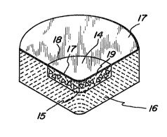
By slicing the composite of Figure 1, the
cutting tool if Figure 3 can be produced with
polycrystalline layer 14 having cutting tool nose 15
of given radius joining straight edges 17 and 19.
ordinarily, edge 19 is a side cutting edge and edge 17
is an end cutting edge. The layer 14 is adhered to a
recessed portion of substrate structure 16.
Specifically, a face of layer 14 is integrally adhered
to the bottom surface of the recessed portion of
substrate structure 16 and its round side 18 is
integrall~ adhered to a wall of the recessed portion.
The top surface of layer 14 is substantially level
with the top surface 17 of substrate structure 16.
FIGURE 4 shows another form of the present
composite wherein integral cemented carbide element 22
of substrate structure 21 has formed four cutting tool
noses of given radii 23, 24, 25, and 26 in
polycrystalline layer 20.
FIGURE 5 shows the cutting tool formed by
cross-sectionally slicing the composite of Figure 4.
Specifically, Figure 5 shows polycrystalline layer 27
with cutting tool nose of given radius 30 joining
straight edges 29 and 31 and that layer 27 is
integrally adhered to a recessed portion of substrate
structure 28.
It is to be understood that the cutting
tools produced by the present invention ~ill, most
usually, be mounted or bonded to a larger body, e.g. a
tool shank or a milling cutter or a drill bit, for
presentation to the material to be cut. The present
cutting tools are useful for grinding or cutting
materials having a harness between about 2 to 9
hardness on the Moh scale. For example, thje present
cutting tools are useful in turning, boring and
~.~7'5~7S
RD 16,820
- 14 -
milling operations on metals such as copper, brass,
bronze, silver, gold, platinum and alloys of aluminum,
magnesium, steels, superalloys, titanium and zinc.
The present cutting tools are also useful in the
machining of non-metallic materials such as plastics,
stone, concrete, composites and ceramics.
The invention is further illustrated by the
following example wherein the procedure was as Eollows:
The substrate structure was comprised of
cemented carbide, i.e. polycrystalline tungsten
carbide cemented with cobalt which was present in an
amount of about 13~ by weight of the cemented carbide
body. The c~mented carbi~e body had a porosity of
less than about 5~ by volume.
The high pressure high temperature apparatus
used was substantially of the same type disclosed in
U.S. Patent No. 3,745,623.
EXAMPLE 1
The composite illustrated in Figure 1 was
prepared in this example.
A cemented carbide disk about 0.125 inch
thick and about 0.35 inch in diameter was subjected to
electrical discharge machining to remove material
therefrom to form a disk-shaped recess in its central
portion. The recess had a diameter of about 0.2 inch
and a depth of about .060 inch.
This substrate structure was fitted into a
molybdenum cup with the recess~containing side
exposed. The recess was then filled with a slight
excess of diamond crystals having an average size
range of about 10-40 ~im with some fines.
The cup was then capped with a disc of
molybdenum and the resulting assembly was placed in
the reaction vessel of the high pressure high
temperature apparatus. The pressure was raised to
about 55 kilobars. The temperature was then raised to
.275~
RD 16,820
- 15 -
about 1450C where it was held for about 10 minutes.
Heat input was then ceased and after the system had
cooled to close to ambient temperature, the pressure
was released. The resulting composite having
molybdenum adhered to its outer surface was then
recovered. The molybdenum deposit was removed from
the composite by grinding.
The composite was surface ground on the flat
faces and the periphery by cylindrical precision
grinding to give the required shape, size and finish.
The polycrystalline diamond layer 11 of the composite
was well adhered in the recess 12 and it was
- ~ubstantialiy level with the surround~ng surface 13 oi
the substrate structure 10. The composite was then
cross-sectionally sliced into four substantially
equivalent finished cutting tools using wire electric
discharge machining. Slicing of the composite along
line 3-3 of Figure 1 illustrates the production of one
of the cutting tools which is shown in Figure 3.
Each resulting cutting tool had a nose 15
with a radius of about .030 inch. The tool nose
joined two straight cutting edges 17 and 19 as shown
in Figure 3. The adhered face and round side 18 of
the polycrystalline layer 1~ of each cutting tool were
strongly adhered to the substrate structure 16. In
each cutting tool, the polycrystalline diamond
layer 1~ had a thickness of about 0.05 inch and a
concentration of diamond greater than about 70% by
volume of the layer.
Each cutting tool, if mounted in a tool
holder, would be useful for cutting materials such as
the abrasive aluminum-silicon alloys.