Note: Descriptions are shown in the official language in which they were submitted.
RD-1~,407 .
IMPROVED SNUBBER ARRANGEMENTS W TH ENERGY
RECOVERY FOR POWER CONVERTERS USING
SELF-EXTINGUISHING DEVICES
The present invention relates in general to
snubber arrangements wherein snubber energy is returned to
the dc supply through a recovery transformer and more
specifically to the resetting of the recovery transformer
following a period OI energy recovery.
Back~round of the Invention
DC to AC power converters are known which use tWO
switching devices connected in series in each leg of the
converter, ~he junction of each series-connected pair of
switching devices comprising an output of the converter.
Such a converter has been used in adjus~able speed ac mo.or
drives where a pulse width modulated three~phase bridge
inverter supplies a voltage of adjustable amplitude and
fre~uency to a motor.
The use of a self-extinguishing power semisonduc-
tor device such as a gate turn-off thyristor (GTO) or a high
power transistor in a power converter reguires both a series
inductive snubber to limit the rate of change of current
with respect to time (di/dt) when turning on and a shunt
capacitive snubber to limit the rate of change of voltage
with respect to ti~e (dv/dt) when turning off. After
switching (either the turning on or turning off of either
switching device of the leg), energy is trapped in the
snubber elements. In the prior art, this energy is usually
discharged through resistors. It is also known to recover
some of the snubber energy, as described in a paper by A.
Ferraro, "An Overview of Low Loss Snubber Technology for
RD-14,407
5~
Transistor Converters", Conference Record IEEE Power Elec-
tronics Specialists Conference, 1982, pages 465-477.
It is also known to recover trapped snubber energy
via a single transformer such that the transformer is loaded
only during commutation transients. This transformer can bs
relatively small and can employ an iron core so that the two
windings can be reasonably well coupled, thus improving the
efficiency of energy recovery. However, in ~he known
configurations of th~ recovery transformer, the reset time,
which is the time it ~akes the flux in the transformer to
reduce to zero, is so long as to impose an unacceptable
upper limit on the frequency at which the transformer can
operate. If the transformer is not reset by the next
commutation, it will saturate. As a result, the snubber
energy will remain trapped as a high magnetizing current
circulating through tne snubber inductance and the saturated
primary winding of the transformer until it is dissipated by
losses. Thus, little if any energy would be recovered.
,.
Objects of the Invention
It is a principal object of the present invention
to provide a new and improved method for restoring snubber
energy to the dc supply in a dc to ac power converter.
It is a further object of the present invention to
provide a method for improving the reset time of the recov-
ery transformer in a dc to ac power converter.
It is another object of the present invention to
provide a new and improved apparatus for resetting the
recovery transformer in a dc to ac power converter.
Summary of the Invention
3a These and other objects are achieved by a method
for restoring snubber energy in a leg of a power converter
--2--
RD-14,~07
~, ~r~iJ5~j9l
to the dc supply following a commutation in the leg. The
leg includes first and second switching devices coupled in
series and first and second feedback diodes coupled in
anti-parallel with the first and second switching devices,
respectively. First and second series inductive snubbers
and first and second shunt capac~tive snubbers are connected
to the first and second switching devices, respectively. A
recovery trans~ormer couples the snubbe-s to the dc supply.
The leg further includes first and second unidirectional
conducting devices which polarize the cnarging and discharg-
ing of the snubbers. The method comprises the steps of
transferring energy from the snubbers to the dc supply
through the recovery transformer, damping out oscillations
between the recovery transformer and t~e one of ~he first
and second shunt capacitive snubbers which holds an over-
charge following the transfer of energy to t~e dc supply,
and dissipating the magnetizing current of the recovery
transformer to reset the recovery transformer following the
trans'er of energy to the dc supply.
Apparatus for restoring snubber energy to the dc
source comprises first and second switching devices and
first and second feedback diodes in anti-p2rallel with the
first and sec~nd switching devices. Each of the switching
devices is connected to a series inductive snubber and a
shunt capacitive snubber. The primary winding of a recovery
transformer couples the first shunt capacitive snubber to
the second shunt capacitive snubber and a secondary winding
of the transformer is coupled across the dc source. A
recovery diode connected in series with a secondary winding
directs recovered energy to the dc source. First and second
unidirectional conducting devices polarize the charging and
discharging of the snubbers. The apparatus further includes
a reset branch coupled in parallel with the primary winding
--3--
RD-14,407
7~
and including a reset resistance connected in series with a
reset diode. The reset branch may further include a reset
capacitor coupled across the reset resistance or at least
one more diode connected in series with the reset diode.
Detaile Descri~tion of the Drawings
The novel features o~ the invention are set for,h
with p3r~ icularity in the appended claims. The invention
itself, howevex, both as to organi~ation and me~hod of
operation, toge~her with further objects and advantages
thereof, may best be understood ~y re~erence to the follow-
ing description taken in conjunction wi.h the accompanying
drawings in which:
F~gure 1 is a schema~_ic diagram showing a prior
art snubber con iguration with an energy recovery transform-
l~ er.
Figure 2 is a schematic diagram of an improved
snubber configuration according to the present invention.
Figure 3 is a schema~ic diagram of another embodi-
ment of ~he circuit shown in Figure 2.
~0 Figura 4 is a schematic diagram of ye' another
embodiment of the circuit in Figure 2.
Figure 5 is a schematic diagram of an embodiment
of the circuit in Figure 2 including a decoupling switch
connected to the energy recovery transformer.
Figure 6A is a schematic diagram of another
e~bodiment of the circuit of Figure 2, and Figure 6B shows
the trigger circuit of Figure 6A in greater detail.
Detailed DescriDtion of the Invention
A known snubber configuration which is shown by T.
Asaeda et al. in "DC-to-AC Power Converter for Fuel Cell
System", Conference Record of Fifth International
-4-
RD-14,~07
5~91
Telecommunications Energy Conference, October, 1983, pages
84-91, is illustrated in Figure 1. A pair of switching
devices 10 and 11 are coupled in series across a source of
dc voltage E. A feedback diode 12 is coupled in
anti-parallel with switch 10 and a feedback diode 13 is
cou?led in anti-parallel with switch 11. The output of this
single leg of a converter is taXen at .erminal 14. Reactors
15 and 15 are series inductive snubbers which limit di/dt
du~ing turn on of a respective switching device 10 or 11.
Capacito-s 17 and 18 comp~is2 shunt capacitive snubbers
which limit dv/dt during ~ne turn-off of a respective
switching device 10 or 11. The charsing and discharging of
the snubbers is polarized by diodes 21 and 22 connected as
shown. Follo~ing a commu.ation of either switching device
10 or 11, snubber energy circulates through diode 23 and
primary winding 2 a of recovery transformer 20. Thus, the
energy is transferred to secondary winding 24b and to the dc
supply through diodes 25 and 26 of a diode rectifier com-
prising diodes 25-28. The pair of diodes 27 and 28 places a
maximum limit on the reset voltage of the transformer, i.e.
the reverse voltage across the transformer following an
energy recovery, while diode 23 i~creases the actual or
threshold reset voltage. As previously described, the long
reset times resulting from the confi~uration shown in Figure
2S 1 limits the maximum frequency of operation of the power
converter. The above-mentioned reference contains a de~
tailed description of the circuit shown in Figure 1.
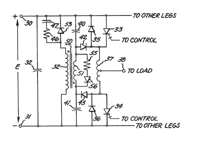
A first embodiment of the present invention is
shown in the schematic diagram of Figure ~. As in Figure 1,
only a single leg of the converter is shown, it being
understood that each of the other legs of the converter are
identical. A dc supply voltage E is provided across ter-
minals 30 and 31 and is filtered by a dc filter capacitor
--5--
RD-1~,407
32. GTOs 33 and 34 comprise the main switching devices of
the leg and are coupled in series across the dc supply. The
gates of GTOs 33 and 34 are connected to a control circuit
(not shown) which is known in the art, such as a pulse-width
S modulation (~WM) con.rol circuit. Feedback diodes 35 and 36
are coupled in an~i-parallel with GTOs 33 and 34, respec-
tively. A center tapped inductor 37 is connected between
GTOs 33 and 34 wi,h tne center tap of inductor 37 providing
an output terminal 38 of the leg shown. Thus, each half of
center tapped inductor 37 provides a series inductive
snubber for GTOs 33 and 34, respectively.
A capacitor 40 is coupled across GTO 33 for
providing a first shunt capacitive snubber and a capacitor
al is coupled a~ross GTO 34 for providing a second shunt
capacitive snuboer. A pair of diodes 4~ and 43 are connect-
ed to capacitors AO and 1, respectively, in series-aiding
fashion with diodes 35 and 36, respectively, to pslarize the
charging and discharging of the inductive and capacitive
snubbers.
An energy recove-y transformer 50 couples the
inductive and capacitive snubbers to the dc supply. Primary
windlng 51 couples capacitor 40 .o capacitor 41. Secondary
winding 52 is connected in series with a diode 53 across the
dc supply. A capacitor 47 and resistor 46 comprise a
snubber for diode 53. Energy recovery transformer 50 is
wound such that an increasingly positive current entering
the dotted terminal of the primary winding induces a posi-
tive voltage at the dotted terminal of secondary winding 52.
Due to the action of diodes 42 and 43, snubber
energy following a commutation of the converter leg flows
through primary winding 51 of energy recovery transformer
50. Energy is fed back to the dc supply during intervals
that diode 53 conducts.
RD~ 07
J~
A.l
When the period of energy recovery ends with diode
53 blocking as a result of the decreasing voltage across
secondary winding 52, current will be flowing through
primary winding 51, diodes 42 and a3 and inductor 37, and
there will be an overcharge on one of the capacitors 40 or
1. During a commut2tion where a GTO is turned on, the
overcharged ca?acitor will be the one across the other GTO,
i.e. the one not turning on. During commutation where a GTO
is turned off, the overcharged capacitor will be across the
~TO which is switching o_f. The energy associated with the
circulating current and the capaci-or overcharge remains
trapped and is not recoverable.
Oscillations on the primary side of energy recov-
ery transformer ~0 following the period of energy recovery
will guickly reduce the current in inductor 37 and the diode
42 or 43 which is connected to the overcharged
capacitor 40 or 41, respectively, will become nonconductive.
This will leave the overcharged snubber capacitor in oscil-
lation with the magnetizing inductance of primary winding S1
via the diode 42 or 43 which still conducts. The voltage on
the overcharged capacitor will swing from overchar~e to
unoercharge, reversing the vol.age on transformer primary 51
and beginning the reset of transformer 50.
It is desirable to make the resetting oscillation
of the overcharged capacitor near-critically damped so that
the reset time is minimized and so that no energy remains to
cause the voltage to swing forward again. This
near-critical damping is achieved according to the present
invention by connecting the series connected pair of reset
resistor 55 nd reset diode 56 in parallel with primary
winding S1.
When the voltage across transformer primary
winding 51 reverses, current begins to flow through reset
RD-14,407
~.~P~ 3~
resistor 55 and reset diode 56. Near-critical damping of
the oscilla~ion between the overcharged capacitor and the
primary winding 51 can be achieved by selecting the value of
resistor 55. Thus, the resistance of resistor 55 should be
less than 1~2 ~LN/CS, where LN is the magnetizing inductance
of t.ansîormer 50 2S measured from the primary winding ;l
and C5 is the capacitance of the snubber capacitor.
Reset diode 56 provides a reset threshold voltage
for faster reset, i.e. dissipation of the transformer
magne.i~ing current. By causing the transformer to reset
more quickly, ~he converter may be operated at a higher
frequency while s~ill main~aining energy recovery.
Figure 3 shows a modification of the circ~it in
Fi~lre 2 wherein an even higher reset voltage threshold is
used to provide for an even faster reset of the energy
recovery transformer. Thus, two additional reset diodes 57
and 58 are connected in series with reset diode 56. The
reset voltage equals the voltage drop across the reset
resistor (the resis~ance of resistor 55 times the
magnetizing current) plus the voltage drop across the reset
diode or diodes. However, this reset voltage is limited by
the voltage at which diodes 2 and _3 will again begin
conducting. Thus, the reset branch comprising the reset
resistor and the reset diode or diodes can damp the oscil-
lations between the overcharged capacitor and the primarywinding of the transformer while the magnetizing current of
the transformer may be dissipated either in the reset branch
or in diodes 42 and 43 and center tapped inductor 37,
depending on the threshold voltage of the reset branch. The
use of three reset diodes as shown in Figura 3 insures that
the magnetizing current is dissîpated in diodes 42 and 43
and inductor 37 since the latter components will conduct
first.
-8-
~ 5 ~ RD-14,~07
Figure 4 shows another modification of the circuit
in Figure 2 for increasing the threshold voltage of the
reset branch without the addition of more reset diodes. In
this case, the voltage of the reset branch is increased by
increasing the value of the resistance of resistor 55. The
increase in resis'ance re~ires the use of a relatively
large capacitance provided by capacitor 60 connected in
parallel wi h resistor 55. Capacitor 60 is preferably a low
voltagQ ele-_rolytic capacitor. It will absorb transient
pulsQs of cur-ent that occur when reset begins and will then
act as a quasi-voltage source.
It ls possible to achieve a higher reset threshold
voltage by decoupling the transformer primary from the
snub~ers and snubber diodes 42 and 43 as shown in Figure 5.
Thus, a reset GT0 65 is connected in series with primary
winding 51. Reset GT0 65 should be turned on-during each
commutation, allowing snubber action and energy recovery to
proceed normally. After diode 53 blocks and the oscil-
lations of the overcharged capacitor have been damped (i.e.
the current in primary winding 51 is reduced to the trans-
former masnetizing level~, reset GT0 65 is switched off.
This forces .he magnetizing current OI the transformer into
the reset branch through resistor 55 and dlode 56, thus
assuring fast reset of the transormer.
Control of reset GT0 65 is provided by a gate
driver A such that reset ~-T0 65 is off during transformer
reset and is otherwise on. Gate driver A is connected
between the gate and cathode of reset GT0 65 and has a
configuration known in the art. Gate driver A may also
comprise an improved gate driver circuit as shown in
United States Patent Number ~ ~93,Z~, issued
by the same inventor as the instant application and assi~ned
to the instant assignee.
RD~ 07
7~
Reset GTO 65 may be relatively small since it is
subjected to only a fraction of the DC source voltage and
its average current is low. Since the current in reset GTO
65 is only the magnetizing current of the transformer at the
turn-off of r2set GTO 6~, it may be successully switched
without a s~u~b~r.
A circuit similar to that in Figure 5, but having
ordinary _hyris.ors ra_her .han a reset GTO is shown in
Figure 6A. Thyristors 66 and 67 replace diodes 42 and 43 of
Fi~ure 2 _o take advantage of the fact that one or the other
of diodes ~2 and 43 is reverse-biased following the period
of energy ~ecovery. Therefore, it is possible to reliably
turn off an or~inary thyristor to decouple primary winding
51 from the sa~lbbels without a turn-off gate circuit. Gate
circuits B, one of which is shown in detail in Figure 6B,
are provided for thyristors 66 and 67. ~ach gate circuit
comprises a zener diode 70, resistors 71 and 72, capacitor
73 and a diode 74. The series combination of zener diode 70
with the par211el-connec~ed pair of resistor 71 and
capacitor 73 is coupled between the gate and the anode of
each thyristor. Tne parallel-connected pair of resistor 72
and dioàe 7 is cou?led between the sate and cathode of each
thyris~or. Zener diode 70 may typically have a breakdown
voltage of 33 volts. Other typical values for gate circuit
~5 B are .05 microfarads for ca~acitor 73, 100 ohms for resis-
tor 71 and 47 ohms for resistor 72. Series connected diodes
68 and 69 are each connected o one of the gate circuits B,
as shown in Figure 6A. In operation, one of the thyristors
66 and 67 will turn off following a period of energy recov-
ery and the magnetizing current of the transformer is
dissipated in the reset branch comprised of resistor 55,
diode 56 and capacitor 60. Gate circuit B is also suitable
-10--
~D-1~,'07
~ 5 ~
for use as the turn-on portion of gate circuit A in Figure
5.
The foregoing describes a method and circuits for
improving the resetting of an energy recovery transformer in
a dc-ac converter. In converters usirg the circuits sf the
preser... inven ion, chopping frequencies of the converter in
excess of 250 her.z are obtainable without saturating the
recovery ~ransformer. This extends the operating range of
the recovery transformer to near the practical frequency
limit for present GT0 devices, which results from their
inte-nal switching losses.
While preferred embodiments of the present in-
vention have been shown and described herein, it will be
obvious to those skilled in the art that such embodiments
are provided by way of example only. Numerous variations,
changes and s~bstitutions will now occur to those skilled in
the art without departing from the invention. Accordingly,
it is intended that the invention be limited only by the
scope and spirit OI the appended claims.