Note: Descriptions are shown in the official language in which they were submitted.
~;~'7~708
SEMICONDUCTOR ~WITCHING CIRCUIT
Field of the Invention
This invention relates to semiconductor switching
circuits and, more particularly, to a semiconductor switching
circuit which converts a light signal into an electrical signal
by means of a photovoltaic diode array optically coupled to a
light emitting element, such as a light emitting diode, which
converts an input signal into a light signal; the converted
electrical signal being utilized for driving an output device
such as a field effect transistor (''FET'I), preferably a metal-
oxide-semiconductor field effect transistor ("MOSFET").
Bac~round of the Invention
There has been proposed in U.S. Patent No. 4,227,098
to Dale M. Brown et al a circuit in which a photovoltaic diode
array is optically coupled to a light emitting diode, electrical-
ly connected in parallel across a resistive impedance, and
further electrically connected in series with the gate and source
electrodes of a MOSFET. When current flows across the input
terminals of the light emitting diode, an output voltage is
generated across both terminals of the photovoltaic diode array,
and is applied across the gate and source of the MOSFET.
Consequently, the impedance of the MOSFET changes to a different
value. In the case of an enhancement mode MOSFET, the MOSFET
switches from the OFF state to the ON state. The resistive
impedance then discharges electrostatic charge accumulated across
the gate and source electrodes of the MOSFET. If no such
resistive impedance is present, the MOSFET will not return to the
OFF state, even when the input current to the light emitting
diode is interrupted.
On the one hand, it is desirable to increase the value
of the resistive impedance in order to reduce the required
minimum input current for switching the MOSFET to the ON state.
~r
. ~ .
7(~3
On the other hand, the resistive impedance is preferably
minimized in order to reduce the time required to turn the MOSFET
OFF after interruption of the input current. These conflicting
goals are difficult to achieve simultaneously. When the input
current is in the minimum current range, the voltage across the
gate and source of the MOSFET varies proportionally to the input
current, so that the output impedance of the MOSFET may take an
intermediate value, causing the MOSFET to assume an intermediate
state between the ON and OFF states, which may cause a large
power loss and consequential damage to the circuit elements.
U.S. Patent No. 4,390,790 to Edward T. Rodriguez
discloses a semiconductor switching circuit in which a photo-
voltaic diode array optically coupled to a light emitting diode
is connected in series with a MOSFET. A normally on type
junction FET is connected to the gate and source of the MOSFET.
An additional photovoltaic diode array is connected across the
gate and source of this junction FET, through a resistor.
According to Rodriguez, the intermediate state of the MOSFET can
be prevented by the provision of an additional diode array for
driving the junction FET. However, the circuit arrangement
required to combina the junction FET with the additional diode
array causes another problem, in that a larger integrated circuit
chip is required for the diode array and the optical conduction
coefficient accordingly deteriorates, resulting in lower
photosensitivity and switching capability of the circuit.
U.S. Patent No. 4,492,883 to William J. Janutka,
discloses a circuit to turn OFF a MOSFET, in which a P-channel
type FET is connected between the gate and the source of the
MOSFET; a Zener diode is inserted between the gate and the source
of the P-channel FET, (i.e., between the gate of the MOSFET and
the gate of the P-channel FET); and a resistor is connected
between the gate and the drain of the P-channel FET. This
circuit arrangement may also inhibit the intermediate state of
the MOSFET. However, in order to achieve high speed switching
operation, it becomes necessary to use a high-voltage, high-
1~7570~3
current power source, which leads to further problems when thecircuit is coupled to a photovoltaic diode array.
One approach to the problem would be to connect a
photovoltaic diode array in series with a hiqh impedance element
between the gate and the source of a ~OS~ET. An ON type driving
transistor could then be connected with its drain connected
between the gate of the MOSFET and the photovoltaic diode array,
its gate connected between the photovoltaic diode array and the
impedance element, and its source connected between the impedance
element and the source of the MOSFET. The voltage developed
across the impedance element due to the current supplied by the
photovoltaic diode array would bias the driving transistor into
a high impedance state. This arrangement prevents the MOSFET
from entering an intermediate state between ON and OFF while
input current is near the minimum value required to switch the
MOSFET ON. This arrangement also facilitates higher switching
speeds than the circuits described in the aforementioned United
States patents. However, this arrangement still suffers a number
of shortcomings. For example, it is desirable to improve the
input sensitivity of the circuit and to further shorten its
response time to achieve higher switching speeds. The sensitiv-
ity of the circuit may be increased by selecting a large value
for the impedance element, thereby reducing the minimum current
required to turn the MOSFET ON. Unfortunately, a large impedance
value increases the time required to switch the MOSFET OFF.
Summary of_the Invention
The object of the present invention is to provide a
semiconductor switching circuit with improved sensitivity and
increased operating speed wherein the state of the output
transistor is prevented from being intermediate between the ON
and OFF states.
According to the present invention, the above object
may be attained by a semiconductor switching circuit in which a
-- 4
. ..
S~()8
photovoltaic diode array is connected in series with a resistor;
both the array and the resistor being further connected between
the gate and source of an output FET. A light-emitting element
which generates a light signal in response to an input current
is optically coupled to the photovoltaic diode array. A
constant-voltage conduction element is connected in parallel
across the resistor. The drain of a depletion mode driving FET
is connected between the photovoltaic diode array and the gate
of the output FET. The source of the driving FET is between the
source of the output FET and the resistor. The gate of the
driving FET is connected between the photovoltaic diode array
and the resistor.
Upon the application of a voltage greater than its
threshold volta~e, the constant-voltage conduction element
becomes conductive. In this improved circuit, the threshold
voltage of the constant-voltage conduction element is selected
so that it is higher than the threshold voltage required to
switch the driving FET from its normal ON state to its high
impedance OFF state. The driving FET can therefore be biased
into the OFF state by a voltage developed across the resistor and
the constant-voltage conduction element due to the flow of
current generated when the photovoltaic diode array receives a
light signal.
The sensitivity of the improved semiconductor switching
circuit described above can be increased by selecting a high
value for the resistor connected between the gate and the source
of the driving FET. When this is done, even a slight input
current will result in a voltage drop across the resistor large
enough to switch the driving FET OFF. With the driving FET
switched OFF, the gate potential of the output FET can be
elevated sufficiently to switch the output FET ON. During the
transient period of this switching operation, the potential at
the drain of the output FET drops from source voltage level to
near zero. This causes a change in the potential difference
between the drain and the gate of the output FET and results in
~.~7~7~3
charge flowing from the gate of the output FET through the
photovoltaic array and through the resistor. The increased
current through the resistor results in a voltage drop across the
resistor and constant-voltage conduction element greater than the
threshold voltage of the constant-voltage conduction element.
The constant-voltage conduction element then begins to conduct
and acts as a bypass to the resistor, maintaining the discharge
current at a high level which depends upon the drain-gate
capacitance of the output FET. Fast switching of the output FET
from OFF to ON is thereby assured.
Other objects and advantages of the present invention
shall be made clear in the following disclosure and accompanying
drawings.
Brief Description of the Drawings
Figure 1 is a circuit diagram of a semiconductor
switching circuit according to the present invention wherein a
Zener diode is employed as the constant-voltage conduction
element;
Figure 2 is a graph showing the relationship between
the value of the resistor and the sensitivity of the circuit (the
minimum input current needed to switch the output MOSFET from OFF
to ON);
Figure 3 is a graph showing the relationship between
the switching speed of a semiconductor switching circuit, with
and without a constant-voltage conduction element, and the input
current;
Figure 4 is a circuit diagram of a semiconductor
switching circuit according to the present invention wherein an
enhancement mode FET is employed as the constant-voltage
conduction element.
~57~
While the invention shall be explained with reference
to the specific embodiments shown in the accompanying drawings,
it should be appreciated that the intention is to cover all
design modifications which come within the scope of the appended
claims rather th~n any specific embodiments.
Description of the_Preferred Embodiment
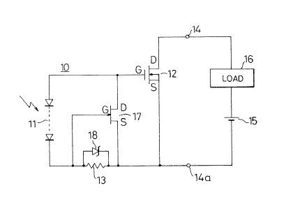
Figure 1 shows an embodiment of the semiconductor
switching circuit of the present invention. The circuit 10
includes an output FET 12 which is preferably a MOSFET, and most
preferably an n-channel enhancement mode MOSFET. The drain and
source of output FET 12 are connected through output terminals
14 and 14a in series with a power source 15 and a load 16.
Current can flow from the power source and through the load when
MOSFET 12 is switched from its high-impedance OFF state to its
low-impedance ON state. For proper operation of the circuit,
power source 15 is connected so as to make the drain of MOSFET
12 positive with respect to the source.
Circuit 10 further comprises a diode array 11, and a
resistor 13 which are connected in series between the gate and
source of output FET 12. Diode array 11 is optically coupled to
a light-emitting element (not shown), such as a light-emitting
diode, which generates a light signal in response to an input
current signal. Resistor 13 has a relatively high value. On
receipt of a light signal from the light emitting element, diode
array 11 generates a photovoltaic output. The current flowing
through load 16 can be controlled by applying the photovoltaic
output of diode array 11 between the gate and source of MOSFET
~2. This causes MOSFET 12 to switch from a first impedance state
to a second impedance state.
The final elements of the circuit are driving FET 17
and Zener diode 18~ Depletion mode driving FET 17 has its drain
connected to the gate of output FET 12, its source connected to
the source of output FET 12 and its gate connected between
1~
~X~757(~8
photovoltaic diode array 11 and resistor 13. Driving FET 17 is
preferably a junction FET (JFET) which can be biased into its OFF
state by a voltage developed across resistor 13.
Zener diode 18 is connected in parallel with resistor
13 and constitutes the constant-voltage conduction element which
is unique to the present invention. 2ener diode 18 is selected
to have a breakdown vol~age higher than the threshold voltage of
driving FET 17. Furthermore, Zener diode 18 is inserted in
circuit 10 with polarity such that when a voltage higher than the
breakdown voltage of Zener diode 18 is applied across Zen~r diode
18, it conducts and the resulting current flow establishes a
charge across the source and gate of output MOSFET 12.
The operation of the circuit shown in Figure 1 will now
be explained. To aid in understanding the present invention, the
operation of a circuit lacking Zener diode 18 will be described
first. A light signal received at diode array 11 causes a
photovoltaic voltage to be generated by diode array 11. This
voltage, in turn, causes a current to flow around circuit 10.
The current flows through driving FET 17, which is normally ON,
through resistor 13, and back to diode array 11. When the
voltage drop across resistor 13 exceeds the threshold voltage of
driving FET 17, the latter switches OFF. Consequently, the
current generated by photovoltaic diode array 11 flows to the
gate of output MOSFET 12 and elevates the potential of the gate
of MOSFET 12 relative to the source. This causes MOSFET 12 to
switch from OFF to ON. During the transient period of this
switching operation, the potential at the drain of MOSFET 12
drops from the level of power source 15 to near zero. The
potential difference between the drain and gate of MOSFET 12
therefore varies greatly, with the result that some of the charge
accumulated at the gate of MOSF~T 12 discharges through diode
array 1~ and resistor 13. The time required for this discharge
is a large fraction of the operation time, or, in other words,
the response time, of circuit 10.
~.~757~)~
In circuit 10, the minimum input current, or working
current, required to turn output MOSFET 12 ON gradually decreases
as the value of resistor 13 is increased. This is shown in
Figure 2. Curves k, 1, and m, trace the combinations of working
current and resistance which result in gate-source voltages at
the driving FET of -0.3V, -0.5V and -0.9V respectively. As can
be seen, the minimum input current to the li~ht-emitting element
which will result in MOSFET 12 turning ON, Ion, decreases as the
resistance of resistor 13 is increased. The working curr~nt is
about 2 mA when the resistance and the required gate-source
voltage are: 1.0 Mn and -0.3V; 1.7Mn and -0.5V; or 3.0Mn and -
O.9V.
As shown in Figure 3, when resistor 13 has a given
value, the response time, Ton, of circuit 10 cannot be decreased
merely by increasing the input current, I~, to the light emitting
element and, consequently, increasing the intensity of the light
shining on diode array 11. Curves n, o and p show the relation-
ship between Ton and If where the value of resistor 13 is 0.3Mn,
1.0Mn and 3.0Mn respectively. It is clear from Figure 3 that
high speed operation of this circuit is very difficult to
realize. For example, if the value of resistor 13 is greater
than 3.0Mn, the response time Ton will exceed 600 ~sec./ even
when the input current to the light emitting element, If, is
greater than 50mA. The slow response is due to the time required
to discharge the charge accumulated on the gate of MOSFET 12,
which discharge is impeded by resistor 13.
In the embodiment of the invention shown in Figure 1,
Zener diode 18 is connected in parallel with resistor 13. If,
while charge at the gate of MOSFET 12 is being discharged, the
voltage across the parallel circuit of resistor 13 and Zener
diode 18 exceeds the breakdown voltage of Zener diode 18, then
Zener diode 18 becomes conductive and the discharge current flows
mainly through Zener diode 18, bypassing resistor 13. With Zener
diode 18 included in the circuit aforesaid, the time for the
charge at the gate of output MOSFET 12 to be discharged can be
_ 9 _
,..~, ~
~'~'757~)~
made small, even when resistor 13 has a large value. Curve Q in
Figure 3 shows that, with Z,ener diode 18 in the circuit, the
relationship between If and Ton is linear. MOSFET 12 can there-
fore be switched at high-speed from its OFF state to its ON state
even when resistor 13 has a large value and the working current
is correspondingly small.
When MOSFET 12 reaches its ON state, the discharge from
the gate of MOSFET 12 terminates, the voltage across the parallel
combination of resistor 13 and Zener diode 18 drops, and the
Zener diode ceases to conduct current. A slight current
continues to flow between the drain and source of driving FET 17
and, due to the presence of resistor 13, driving FET 17 is
maintained in its high impedance state.
When the input current to the light emitting element
is cut off, photovoltaic diode array 11 ceases to receive a light
signal, the photo~oltaic output of diode array 11 is interrupted,
and the voltage between the gate and ~ource of driving FET 17
drops. Driving FET 17 then returns to its ON state, allowing the
charge which has accumulated at the gate of MOSFET ~2 to be
quickly discharged through driving FET 17. MOSFET 12 is thereby
switched into its OFF state and a high impedance results between
terminals 14 and 14a. While the charge accumulated at the gate
of driving FET 17 must be discharged through resistor 13 before
driving FET 17 can return to its ON state, the time required is
short because the capacity of the gate of driving FET 17 is much
smaller than that of output MOSFET 12. Therefore, the time taken
to discharge driving FET 17 does not substantially impair the
high-speed operation of circuit 10.
Figure 4 shows an alternative semiconductor switching
circuit according to the present invention. Each circuit element
which appears in both Figures 1 and 4 is denoted in Figure 4 by
a numher which is 100 larger than the corresponding label in
Figure 1. The circuit of Figure 4 differs from that of Figure
1 only in that the constant-voltage conduction element in
-- 10 --
7~
parallel with resistor 113 is an enhancement mode FET 118 with
its gate and drain short-circuited. The threshold voltage of F~T
118 is selected so as to be higher than the threshold voltage of
driving FET 117. FET 11~ is connected in parallel across
resistor 113 and between the gate and source Gf driving FET 117
with polarity such that when FET 118 conducts current, a charge
is developed across the gate and source of MOSFET 112.
As the voltage across the parallel combination of
resistor 113 and enhancement mode FET 118 rises past a predeter-
mined threshold voltage, the path between the drain and source
of FET 118 begins to conduct~ Because of the short circuit
between the gate and the drain of enhancement mode FET 118, FET
118 performs substantially the same function in the circuit of
Figure 4 as does Zener diode 18 in the circuit of Fig. 1. A
particular advantage of the embodiment of the invention shown in
Fiure ~ is that enhancement mode FET 118 is similar in structure
to MOSFET 112 and driving FET 117 This simplifies the process
of fabricating circuit 110 on a single chip and makes it easier
to mass produce circuit 110.
Other aspects of the operation and arrangement of
semiconductor switching circuit 110 shown in Figure 4 are
substantially the same as the corresponding aspects of circuit
10 shown in Figure l.
In the present invention, a variety of design modifica-
tions may be made to the circuits within the scope of the
appended claims. For example, while the circuits discussed above
use a MOSFET for the output transistor, a static induction type
transistor (SIT) may be used instead. The junction FET (JFET)
used as the depletion mode driving FET 17 or 117 may be replaced
by a depletion mode MOSFET or a static induction type transistor
(SIT). Further, it may be possible to use a P-channel or
depletion mode MOSFET in place of t.he N-channel enhancement mode
MOSFET 12 or 112.
According to the present invention, a semiconductor
switching circuit which is both very sensitive and which is
capable of high speed switching operation can be constructed as
described above. The output FET can be switched from OFF to ON
with a very small input current and yet the eharge at the gate
of the output FET can be quickly discharged, redueing the
transient period required for the output FET to switch into the
ON state. The prior art semiconduetor switching circuits
discussed above have not been able to simultaneously offer these
two antinomic capabilities.