Note: Descriptions are shown in the official language in which they were submitted.
~;~7Sl~S~
INTEGRATED THERMAL INK JET PRINTHEAD
AND METHOD OF MANUFACTURE
Technical Field
This invention relates generally to thermal ink
jet printing and more particularly to a novel thermal ink
jet printhead with improved resistance to ink penetration
and corrosion and cavitatlon wear. This invention is also
directed to a novel integrated circuit which combines print-
head interconnect metal~zation with MOS pulse drive circuit
metalization in a unique multilevel metal MOS integrated
circuit structure.
Back~round Art
Thermal ink jet printing has been described in
many technical publication~, and one such publication rele-
vant to this invention is the Hewlett PacXard Journal,
Volume 36, Number 5, May 1985
In the manu~acture of thermal ink jet printheads,
it i5 known to provide conductive trac s of aluminum over a
~2~5~S4
chosen resistive material, such as tantalum-aluminum, to
provide electrical lead-in conductors for conducting current
pulses to the lithographically defined heater resistors in
the resistive material. These conductive traces are formed
by first sputtering aluminum on the surface of a layer of
resistiva material and thereafter defining conductive trace
patterns in the aluminum using conventional photolitho-
graphic masking and etching processes.
It is also known in this art to deposit an inert
refractory ~aterial such as silicon carbide or silicon
nitride over the aluminum trace material and the exposed
resistive material in order to provide a barrier layer
between the resistive and conductive materials and the ink.
This ink is stored in individual reservoirs and heated by
thermal energy passing from the individually defined resis-
tors and through the barrier layer to the ink reservoirs
atop the barrier layer. The ink is highly corrosive, so it
is important that the barrier layer be chemically inert and
highly impervious to the ink.
In the deposition process used to form the barrier
layer for the above printhead structure, rather sharply
rounded cont~urs ar~ produced in the barrier layer material
at the edges of the conductive aluminum traces. These
contours take the form of rounded edges in the silicon
carbide layer which fir6t extend laterally outward over the
8~
edges of the aluminum traces and then turn back in and down
in the direction of the edge of the aluminum trace at the
active resistor area. Here the silicon carbide barrier
material forms an intersection with another, generally flat
section of silicon carbide material which is deposited
directly on the resistive material. This intersection may
be seen on a scanning electron microscope (SEM~ as a crack
in the barrier layer material which manifests itself as a
weak spot or area therein. This weak spot or area will
often become a source of structural and operational failure
when subjected to ink penetration and to cavitation-produced
wear from the collapsing ink bubble during a thermal ink jet
printing operation.
In addition to the speciic problem with the
above prior art approach to thin ~ilm resistor substrate
~abrication, it has been found that, in general, thin films
and fluidic cavities in thQse structures which have been
optimized for superior printing speed and print quality
suffer from short printing resistor operating life. This is
especially true when large over-energy tolerance is
req~ired. Resistor aging curves taken throughout the
printing life of a thermal ink ~et heater resistor reveal
strongly two mechanisms which contribu~e ~o the early demise
of the heater resistor. One is rapid resistor value
increase due to electrochemical and mechanical inter~ctions
near the resistor terminations. The ~econd is a slow but
~.Z7S85~
continuous increase of the resistance caused by the inter-
face oxidation with the thermal standoff layer and a passi-
vation layer. Simply stated, any mechanism con~ributing to
the increase of the resistor value in ohms is a mechanism
that leads toward the final resistor failure when its value
is infinite.
Disclosure of Invention
Accordingly, the general purpose of this invention
is to provide a new and improved thermaI ink jet printhead
structure and method of manufacture which, among other
things, eliminates the above cracks in the barrier layer
material and thus overcomes the associated problems of ink
penetration through and undue cavitation wear in the barrier
layer. To accomplish this purpose, the resistive heater
layer for the printhead structure is ~ormed of either poly-
cry~talline silicon or a refractory silicide, such as tanta-
lum silicide or titanium silicide or tungsten silicide or
molybdenum silicide. ~hereafter, conductive trace material
of a re~ractory ~etal such as tungsten or molybdenum is
deposited on the rèsistive heater layer. The~, a barrier
layer of silicon dioxide is deposited over the conductive
trace material using chemical vapor deposition (CVD) tech-
niques and then reflowed to form smooth contours in the area
of the barrier layer above the edges of khe conductive trace
material. Finally, an outer protective metal layer such as
il~Z~5~5~
tantalum is sputtered on top of the reflowed silicon dioxide
barrier layer material to provide even further isolation
against ink penetration and cavitation-produced wear of the
structure.
In a modified embodiment of my invention, the
above novel printhead structure is integrated with pulse
drive circuitry, such as metal-oxide-silicon-field-sffect
transistor (MOSFET) dri~ers, in a novel multi-level metal
integrated circuit. In this integrated circuit, a first
level of metalization comprises a refractory metal such as
tungsten, titanium, tantalum or molybdenum which is
patterned to define one dimension of a printhead resistor in
a resistive layer on which it lies. A passivation layer or
layers are dsposited on the first level of metalization and
selectively etched to provide an opening or openings
therein. Then, a second level of metalization, such as
aluminum, i~ deposited in this opening or openings to make
electrical contact with the ~irst level of metalization and
thereby provide an interconnect path between the printhead
resistor and MOSFET pulse drive circuitry and the lik~.
Thus, MOS or even bipolar transistors or other semiconductor
devices may be fabricated in one area of a silicon substrate
and printhead resistor~ defined in another area atop the
surface o~ ~he same silicon substra~e. Then, using the
above multi level interconnect scheme, aluminum intercon-
~27~i8~i4
nects from the outputs of these transistors may beconnected to the refractory metal connections which lead
into the various printhead resistors in novel MOSFET
driver-ink jet printhead integrated circuit
construction.
Various aspects of this invention are as
follows:
A process for fabricating a printhead
structure for a thermal ink jet printhead which includes
the steps of:
a. providing an insulating substrate layer,
b. depositing a layer of resistive material
on the surface of said substrate layer and
consisting of either polycrystalline silicon or a
chosen refractory silicide selected from the group
of tantalum silicide, titanium silicide, tungsten
silicide and molybdenum silicide,
c. forminy a chosen refractory metal
conductive pattern atop said resistive material and
having an opening therein defining one dimension of
a thermal ink jet resistor and for receiving
current pulses when heating said resistive material
during an ink jet printing operation,
d. depositing a layer of silicon dioxide atop
said conductive trace material, and thereafter
e. reflowing said silicon dioxide layer in
order to reshape the contours thereof and enable
the surface contour of said silicon dioxide layer
to more closely replicate the conductive trace
material over which it is deposited.
~ process for fabricating an integrated
thermal ink jet and driver circuit including the steps
of:
A
~L~7S854
a. providing a chosen resistive material on a
printhead substrate,
b. forming a layer of refractory metal on the
surface of said resistive material and having an
opening therein defining one dimension of a thermal
ink jet resistor,
c. providing a passivation layer or layers on
the surface of said refractory metal and having an
opening therein exposing a surface area of said
refractory metal,
d. reflowing said passivation layer or layers
at a chosen elevated temperature to provid~ smooth
contours therein which are compatible with multi-
level metal integrated circuit connections, and
e. depositing interconnect metallization in
said opening to make electrical contact with said
refractory metal, whereby MOS driver circuitry and
the like may be fabricated on a common substrate
with said thermal ink jet heater resistors in a
monolithic multi-level metal integraked circuit
arrangement especially well suited for multi-level
metal interconnections.
~n integrated circuit wherein driver circuitry
and printhead resistor interconnect circuitry are
fabricated on a common substrate, including:
a. a substrate having a layer of resistive
material thereon, said resistive material being
selected from the group consistiny of
polycrystalline silicon and a refractory metal
silicide,
b. a layer of refractory metal disposed on
said resistive material and having an opening
therein defining one dimension of a thermal ink
jet resistor, said refractory metal being selected
6a
A
~27S8S~
from the group consisting of tungsten and titanium
and tantalum and molybdenum,
c. a passivation layer or layers disposed on
the surface of said refractory metal and having an
opening therein exposing a surface area of said
refractory metal,
d. driver interconnect metallization disposed
in said opening in said passivation layer and in
electrical contact with said refractory metal,
whereby said interconnect metallization and said
refractory metal may be formed in immediately
adjacent layers in an MOS multi-level metal
integrated circuit, and
e. a metal barrier layer disposed on the
surface of said passivation layer or layers and
above an ink jet resistor to provide enhanced
insulation from ink which is disposed above said
thermal ink jet resistor, said metal barrier layer
is tantalum, said interconnect metallization is
aluminum, and one of said passivation layers is
phosphorous doped glass.
The advantages and novel features of the above
summarized printhead structure and integrated circuit
will become better understood and appreciated with
reference to the following description of the
accompanying drawings.
Brief DescriPtion of the Drawinqs
Figure l is a schematic cross section view of
the printhead device structure according to a preferred
embodiment of the invention.
Figures 2A through 2G illustrate schematically
the processing sequence used in the manufacture of the
printhead structures in Figure 1.
6b
A
~s~s~
3est Mode for Carrvinq Out the Invention
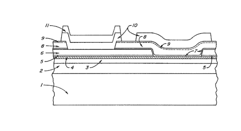
Referring now to Figure 1, the printhead device
structure according to a preferred embodiment of the inven-
tion will be initially described by identifying the various
layers therein. Then, with reference to Figure 2A through
2G, the various process steps utilized in achieving this
device structure will be described in more detail.
In Figure 1, the printhead substrate starting
material 1 is silicon and ha~ a surface thermal isolation
layer 2 o~ silicon dioxide thereon. A silicon nitride layer
6c
~Z751~54
3 is deposited on the surface of the silicon dioxide layer
2, and then a resistive layer 4 of tantalum silicide is
deposited on the surface of the silicon nitride layer 3 to
provide the layer material ~or the resistive heater elements
in a geometry to be further described.
The next two lay~rs 5 and 6 are both tungsten, and
a layer of silicon nitride 7 is formed on the top surface of
the second and thicker layer 6 of tungsten and photolitho-
graphically defined in the geometry shown to determine the
lateral extent of the heater resistor. Next, a layer 8 of
phosphosilicate glass is formed atop the silicon nitride
layer 7, and then another layer of more lightly doped phos-
phorous glass 9 is formed on the previous glass layer 8.
The dielectric passivation layers 7, 8 and 9 are now
appropriately etched using a dry etchant such as SF6 and
argon.
A layer 10 of tantalum is deposited atop the
glass layer 9 and then a further conductive layer 11 of
aluminum is deposited onto the tantalum layer 10. These
interconnection layers 10 and 11 are subsequently etched to
define the two surface barriers for the heater resistor and
the interconnect pad, respectively, on the right and left
hand ~ides of the device structure. These conductive layers
and 11 on the left hand side of Fiyure 1 serve as an
electrical interconnection to other electronics, such as
~27585~
pulse drive circuitry for the heater resistors designed in
layer 4. Thus, the heater resistors in Figure 1 may be
electrically connected by way of tungsten layers 5 and 6 and
through the conductors 10 and 11 on the interconnect pad
side of the structure in a metal-oxide-silicon (MOS)-print-
head integrated circuit o~ novel construction. For example,
the metal contact 11 may be extended in the form of a strip
of metallization to the output or drain terminal of a MOS
driver field-effect transistor which operates as an output
device of a particular MOS pulse drive circuit.
Referring now to Figures 2A through 2G, the sili-
con substrate 1 will typically be 15 to 25 mils in thickness
and of a resistivity of about 20 ohm centimeters and will
have a layer 2 of thermal silicon dioxide of about 1.6
microns in thickne~s thereon as shown in Figure 2A~
In Figure 2~ there is shown a thin 0.1 micron
silicon nitride, Si3N~, layer 3 which is deposited on the
SiO2 layer 2 by low pressure chemical vapor deposition
(LPCVD). This and other similar processes referred to herein
are generally well known in the semiconductor
processing arts and are disclosed for example by A. B.
Glaser, et al. in a book entitled Integratqd Circuit
EnaineQrin~ Desiqn, Fabricati n and Application, Addison-
Wesley, 1979 at pago 237.
Next, as shown in Figure 2C, a resistive layer 4
is formed on the Si3N4 layer 3 by sputtering tantalum sili-
~s~s~
cide to a thickness of between 500 and 1000 angstroms, andthis step is followed by the sputtering of a layer 5 of
tungsten to a thickness of about 250 angstroms. Next, a
thicXer, lower resistivity tungsten layer 6 is grown on the
thin tungsten layer 5 to a thickness of about 0.5 microns by
using chemical vapor deposition (CVD). Then, after etching
the conductive and resistive layers 4,5, and 6 previously
deposited and in the geometry shown, plasma enhanced chemi-
cal vapor deposition (PECVD) is used to deposit a layer 7 of
silicon ni.tride, SiNXHy, of approximately 1000 angstroms in
thickness on the surfacQ o~ the tungsten layer 6 as shown in
Figure 2D. These PECVD processes are known to those skilled
in the semiconductor processing arts and are described, for
example, by R. F. Bunshah et al in an book entitled
Depo~ition Technolo~ies fo~ Films and Coatinas, Noyes
Publications, 1982, page 376 et seq.
In the next ~tap shown in Figure 2D, a layer 8 of
phosphorous doped glass, SiO2, doped to approximately 8
percent phosphoroua content ls formed by chemical vapor
deposition (CVD) in the contour shown, whereafter the struc-
ture i~ annealed for approximately 15 minutes at 1000C to
stabilize a tantalu~ silicide re~lstlve layer 4 and to
reflow the phosphorou~ dope~ or phosphosilicate gla~s (PSG)
over the resistor terminations. Then, a layer 9 of phospho-
~Z7S85~
silicate glasc i~ formed on the surface of layer 8 to athickness of about 2000 angstroms and doped at 4 percent
phosphorous content. This PSG layer 9 is shown in Figure 2E
and serves to inhibit the formation of phosphoric acid which
could attack subsequently applied aluminum final conductors.
At this point in tha process, the triple layer
passivation (7, 8 and 9) is dry etched down to the CVD
tungsten layer as shown at reference number 6 in Figure 2F.
Then, cavitation barrier 10 of tantalum and the final
aluminum interconnect layer 11 are sputtered respectively to
thicknesses of about 0.6 microns and 0.4 microns. These
steps are illustrated schematically in Figure 2G and
complete the resultant structure which corresponds
identically to the composite integrated circuit structure of
Figuxe 1. The pad or interconnect layers 10 and 11 are
patterned by wet chemical etching techniques to define the
device goemetry shown in Figure 2G.
Thus, there haa been described a novel printhead
device structure and method of manufacture wherein
refractory local interconnect metalization, to wit: tung-
sten, allows high temperature reflow of the subsequently
deposited phosphorous doped silicon (PSG) glass, thereby
sealing the resistor electrode terminations. Silicon nit-
ride films are formed above and below the resistor film and
thus serve as effective oxidation barriers while the over-
lying silicon nitride serves as an additional moisture
3 ~Z7S85~
barrier. The refractory silicide resistor film exhibits
superior high temperature stability a~ well as the ability
to anneal the ~tructure up to 1100C before applying the
interconnect metalizatlon.
The above ~tructure and its silicide layer are
compatible with integrated circuit processing and allow the
building of the resistor, conductor and passivation layers
after the resistor logic and drive transistors have been
fabricated. One very signi~icant advantage of this inven-
tion is the fact that a single common semiconductor sub-
strate such as silicon may be used for the fabrication of
MOS or bipolar driver transistors in one area of the sub-
strate and for the fabrication of thermal ink jet printhead
resistors in another area of the substrate. Then these
dQvices may be interconnected using the above described
multi-level metal interconnect scheme.
There are many techniaal references on the per se
use of silicides as the gate level interconnect material for
MOS devices, and such interconnect techniques were discussed
in detail at the 1985 Semicon/East con~erence in Boston,
Massachuset~s in September of 198S. In addition, for fur-
ther reference to certain other applications, treatment, and
deposition of silicides, tungsten metalization and phospho-
silicata glass (PSG), r~ference may be made to the following
technical articles.
A
7~i~S~
TECHNICAL REFERENCES
Tunasten Metalization
N. Susa, S. Ando, S. Adachi, Journal of the Electrochemical
Societv, Vol. 132, No. 9, p. 2245
M. L. Green, R. A. Levy, _ournal of the Electrochemical
Society, Vol. 132, No. 5, p. 1243
Silicides
T. P. Chow, W. Katz, R. Goehner, G. Smith, Journal of the
Electrochemical Society, Vol. 132, No. 8, p. 1914
M. Tamielian, S. Blackstone, Journal of the Electrochemical
Society, Vol. 132, No. ~, p. 1487
R. A. Levy, P. K. Gallagher, Journal o~ the Electrochemical
Societv, Vol. 132, No. 8, p. 1986
S. P. Murarka, "Silicides for VLSI Applications'~, Academic
Press, NY (1983)
T. P. Chow, IEEE Electron Devices, ED-30, 1480 (1983)
PhosPhosilicate Gla~s tPSG)
K. Nassau, R. A. Levy, D. L. Chadwick, Journal of the
Eleatrochemical Societ~, Vol. 132, No. 2, p.409
The following table lists the ~ormation method,
thickness and physical propertie~ o~ the various layers o~
my pre~erred embodiment in accordance with the best mode
known to me at the present time for practicing the inven-
tion.
~2~585~
TABLE OF THIN-FILM MATERIALS AND PROPERTIES
FILMFORMATION METHOD THICKNESS _ PHYSICAL PROPERTY
sio2thermal oxidation 16000 A index of refraction 1.46
Si3N4 LPCVD 1000 A index o~ refraction 2 . Ol
TaSixco-sputter/sinter ~750 A sheet resistance 37 ohm/square
W sputter 250 A sheet resistance 8 ohm/square
W LPCVD 5000 A sheet resistance 0.14 ohm/square
SiNxHy PECVD 1000 A index of refraction 2.00
SiO2/8%PCVD 8000 A index of refraction -1.46
Sio2/4%PCVD 2000 A index of refraction ~1.46
Ta sputter 6000 A sheet resistance 2.7 ohm/square
Al/4%Cusputtex 4000 A sheet resistance 0.12 ohm/square