Note: Descriptions are shown in the official language in which they were submitted.
1276242
A WIDE: BAND IND~7CTIVE TRANSDERMAL
POI~ER AND DATA LINK
The present invention is directed generally to the field of medical
electronics, and more particu]arly to a method and apparatus for
5 conveying power and data through the skin of a subject without
breaking the skin.
With the increase in use of implanted electronic devices beneath
human skin, it has been increasingly desirable to be able to convey
power and/or data to the implanted device without puncturing the
10 skin. A typical approach previously followed was to use a percu-
taneous plug which could deliver power, but must break the skin to
reach the stimulator. Breaching the skin provides a potential path
for infection to enter, risking the safety of the individual as well as
the implant. Another alternative is to implant a battery. t~nfor-
15 tunately, many applications require more amp hours than a batterycan provide without frequent reimplantation.
The use of an inductive link has neither of these limitations since it
leaves the skin intact and can draw from an outside power source.
For medical applications, an inductive link is usually composed of
20 two pancake shaped coils, one implanted in the body and one out-
side the body. These coils form a transformer through which ener-
gy can be sent. Inductive links are already used to deliver power
and information into implanted stimulators. Examples of this can be
found in the Ph.D. Dissertation of M. Soma, "Design and Fabrica-
25 tion of an Implantable Multi-channel Neural Stimulator" Ph.D. Dis-
sertation June, 1980; the Ph.D. Dissertation of T. Gheewala, "A
CMOS Implantable Auditory Prosthesis tlsing Integrated Circuit
Technology," Stanford t~niversity, March 1976, and the article by
$
` ~276242
E.S. Hochmair, IEEE ~ransactions on Biomedical Engineering, Vol,
BME-31, No.2, pp.l77-186, February 1984, entitled, "System Optimi-
zation for Improved Accuracy in Transcutaneous Signal and Power
Transmission, n
5 However, inductive links as considered in these prior efforts have
their own set of difficulties. In the past, these ]inks have had
prob]ems providing efficiency, bandwidth, and insensitivity to
misa]ignment .
It is an objective of the present invention to provide a new and
10 improved inductive link.
It is another objective of this invention to provide such a link
whose gain is relatively insensitive to coupling variations between
the coils which occur with relative movement between the coils.
Yet another objective of the present invention is to provide an
15 inductive link which has a relatively wide bandwidth.
Efficiency is one of the major problems to be attacked in designing
such coup]ing systems. Efficiency is a prob]em because the freedom
of the imp]anted person is limited by the portability of the trans-
mitter power source. If the transdermal link is inefficient, an
20 implant of even modest power demand may require a large amount of
power to the transmitter. If the system requires an excessive
amount of power, the individual must carry a large battery pack.
For example, the systems described in the above-referenced Ph.D.
theses required a battery pack about the size of a brick which
25 needed recharging every eight hours.
Therefore, it is an objective of the present invention to provide a
system which is small and efficient enough for a person to wear
freely and use in everyday activities.
Inductive links have been inefficient because designs to compensate
30 for coil misalignment have been inefficient. ~he coils can move
1276242
3 61051-1952
relative to one another. As they move, their gain (voltage gain,
current gain, transconductance gain, or transimpedance gain,
depending on the input and output circuitry) changes, since their
coupling depends on their relative positions. Many applications
require a stable internal power supply, and therefore, must
regulate the output of the receiver coil.
If the gain variation is too large, the most of the
received power is not used in the stimulator, but wasted in the
voltage regulator coupled to the receiving coil \
The most commonly used approach to solving this problem,
called the geometric approach, sacrifices the coupling magnitude
in exchange for reduction in the coupling variation. It uses an
external coil which iæ larger than the implanted coil. As long as
the small coil remains within the perimeter of the larger coil,
both coils will share roughly the same number of flux lines, and
the coupling will remain fairly constant. The coils can move
laterally and even tilt somewhat with only a minor effect on their
gain. ~his approach is adopted in one or more of the above
references.
Unfortunately, in addition to being inefficient, the
geometric approach is still sensitive to changes in coil
separation; for a small separation (near field), the coupling
drops proportionally with separation. If the coil separation
doubles, then the gain is cut in half. This approach, therefore,
only partially deæensitizes the link gain to the coil's position.
Secondly, in exchange for partially controlling the
gain, the geometric approach sacrifices the magnitude of the
coupling, which raises the lo~ses in the primary coil. Since
, .. .
~276~:42
3a
61051-1952
these coils share fewer flux llnes than two equally sized coils,
their typical coupling coefficient is lower than their equally
sized counterparts. In fact, their coupling is much lower since
their shared area diminishes as the square of the lateral
misalignment tolerance, i.e., shared area -n(larger radius-
alignment tolerance) . Lower coupling requires a higher current
in the primary coil to provide the same output from the
~2762A2
--4--
receiver coil; and higher current wastes more power due to the I2R
losses of the transmitter coil.
The earlier links also had another problem, i . e ., poor bandwidth .
These links were usually single tuned (transmitter coil only) or
5 double tuned (both coils) to the carrier frequency 60 that they
cou]d be driven by a semi-passive RF transmitter (Class C, for
example) for higher efficiency. Semi-passive transmitters need a
high Q tuned circuit to operate efficiently. ~1nfortunately, the
higher the Q, the smaller the band width. The previous Stanford
10 stimulators used a separate ultrasonic data link to obtain a wide
band data path, but that link proved much less tolerant to misalign-
ment than the inductive link, and unreliable in use due to acoustic
impedance mismatches. Clearly, an efficient wide band power and
data link would solve some difficult problems.
15 In summary, the new approach described in the present invention
utilizes a pair of coils, one beneath the skin and one outside the
skin, each connected to a capacitor. The values of the capacitor and
coil inductance are selected to provide a stagger-tuned link. That
is, the values of the components are selected to place the pole of
20 one filter above the operating frequency, and the pole of the other
filter below the operating frequency of the link. The poles will
move as the coupling coefficient changes, desensitizing the link to
the coupling so that the coils can be misaligned in any manner with
little effect on the output.
25 The present invention includes a number of approaches which differ
from obvious uses of stagger tuning or any prior art approaches.
The problem is that when the coils move, the coupling coefficient
changes and so does the ratio of input to output. The present
invention applies stagger tuning to desensitize the link going into
30 the coupling coefficient rather than broaden the band width as is
normally done in stagger-tuned filters.
Second, the gain is stabilized due to an approach which takes into
account and relies on the interaction of two components; typically,
~1.27624~
5 61051-1952
gain is stabilized by isolating components from affecting one
another.
In a further departure from the approaches of the prior
art, a fully active driver or class D amplifier is preferably
utilized to effectively drive the link with a square wave signal.
This signal can be modulated to convey data information to the
implanted receiver coil beneath the skin.
In accordance with a broad aspect of the invention there
is provided an inductive link for conveying power and/or data
through the skin of a user comprising a first external coil, a
second medically implantable coil, the coils being movable
relative to one another, the mutual inductive coupling of said
coils changing with their position relative to one another, and a
means for stagger tuning said first and second coils to maintain a
gain which is relatively independent of the coil's mutual coupling
at a selected frequency or frequency band of interest.
Other advantageq of the present invention will become
apparent from the following detailed disclosure given with
reference to the accompanying drawings wherein:
Figure 1 illustrates the various coil misalignments
dealt with by the present invention,
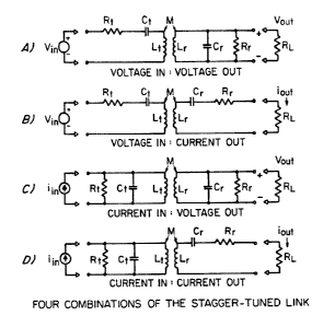
Figures 2A through 2D show the four possible
comblnations of stagger-tuned links,
Figures 3A to 3C illustrate the effective result of a
coupling compensated link voltage device using the circuit
combination shown in Figure 2A,
Figure 4 is a second graph illustrating the effective
relationship of gain versus coupling and load impedance at a given
B
~L276242
Sa
610S1-1952
operating frequency of 20 MHz, and
Figure 5 is a detailed schematic of a Class D
transmitter useful in driving the link of the present invention.
The "Voltage Driven:Voltage Out" link of Figure 2A will
illustrate the approach of the present invention to gain control.
The voltage gain across an untuned or singly tuned two-coil system
varies linearly with the coupling coefficient (assuming the load
resistance is large compared to the coil reactance), so if the
coupling increases by a factor of three, it will cause the voltage
gain to triple. Thls lax galn control is generally unacceptable
because it usually wastes most of the received power in the
voltage regulatlon.
Flgure 2A is a schematic of the transmitter and receiver
elements
~276242
--6--
of an inductive link (Lt and Lr), the tuning
elements (or=l/~Fr and ~t=l/-/L~ the transmitter loss and
receiver load elements (Rt and Rr) and the transmitter source and
receiver voltages. This circuit reduces the coupling dependent gain
5 variation by tuning the coils to two different frequencies; one above
and one below the operating frequency. If these coils' resonances
are placed optimally, their effective poles will shift as the mutual
coupling of the coils changes. The gain wi]] be compensated as a
resu]t .
10 The nvo]tage driven:voltage out" link will help illustrate the new
approach to gain control. Figure 3 is a plot of the voltage gain
versus frequency and coupling for a link that was designed to ope-
rate at 20 MHz. The numbers on the curves represent the values
of coupling coefficient; 2 means K=O . 2, 3 means K=O . 3, and so on .
15 The link is stagger-tuned; i.e., the component values are selected
as shown so that one pole is placed above the operating frequency
(20 MHz) and one pole below. The poles move as the coupling coef-
ficient changes. If they are placed properly, their positions move
to compensate for the changing coupling. To illustrate, in Figure 3
20 as the coupling increases, the poles move away from the operating
frequency, Increased coupling would normally raise the gain at 20
MHz, but the higher coupling has moved the po]es away from the 20
MHz operating frequency, therefore lowering the gain at the operat-
ing frequency. The net result, for this example, is that even
25 though the coupling coefficient changes by 250%, the gain changes
by les~: that ~10%.
Since this approach is based on coupling, not geometry, it not on]y
corrects for latera] displacement and tilt, as did the prior art
geometric approach, but it also handles coil separation, which the
30 geometric solution did not,
Also notice that the gain changes smoothly around the operating
frequency (20 MHz), giving a stable gain over a relatively large
frequency band. Classically, ~tagger tuning has been used to
1276242
7 61051-1952
increase the bandwldth of a system without excessively loading the
tuned circuits. As the example of Figure 3 shows, the new
approach to gain control has carried over the attractive feature
of a wide bandwidth. For many applications, the additional
bandwidth can simplify the design. For example, power and data
links are combined into one inductive link by sending power on the
carrier and the data by frequency-modulating tFM) the carrier as
discussed in U.S. patent No. 4,592,359 of Galbraith, et al.
entitled "An Eight Channel Implantable Neural Stimulator".
This example has clearly demonstrated a wide link gain
which i8 coupling-insensitive. With these capabilities, the power
lost across the internal voltage regulators of an implanted
stimulator can be reduced by taking advantage of the stable gain.
By uslng equal sized coils, lnstead of the mismatched coil sizes
of the geometrlc approach, the average coupling can be improved
which lowers the tranæmitter coil I2R losses. The coupling-
compensated llnk not only allows improved efflciency, but it also
provldes a large bandwldth, something that the previous approaches
have sacriflced for efflclency.
To take advantage of the efflclency afforded by the
- stagger-tuned llnk's stable galn, the link needs a transmitter
that can efflclently handle a variable load impedance whlle
malntalnlng a constant drlving voltage or current. Seml-passive
drlvers, such as class C or claæs E, are not practical because
they lose efficiency if the load impedance is not resonant at the
operating frequency, a fundamental lncompatibility with stagger
tuning. A class D transmitter, on the other hand, can drive these
loads efficiently, and can supply a constant driving source so
J
~L276242
7a
~ 61051-1952
that the link output voltage, or current, remains stable.
A class D transmitter, on the other hand, can drive
these loads efficlently, because it can supply a constant source
which is independent of the load. It simply switches the input of
the link between the two terminals of the power supply. Reactive
loads and
~2762A2
load variations, due to changing coup]ing, should not affect its
output level.
This driver also has a theoretical maximum efficiency of 100%, mean-
ing that its efficiency is not bounded by a sub-optimum theoretical
5 limit, an advantage in any design. The driver's loss is proportional
to the ratio of the voltage dropped across its switches to the supply
voltage. It is fairly simple to make this ratio quite small, and in
practice, the design tends to become more efficient as the output
power level is raised. In fact, the efficiency improves when it is
10 needed most, when the transmitter is delivering the maximum power.
The class D driver, therefore, meets the requirements for driving
the stagger tuned link; it can efficiently drive a variable load with
a stable source.
A class D driver has another advantage due to its square wave out-
15 put. The Fourier Series of a square wave has a fundamental sine
wave whose amplitude is 4/7r times the amplitude of the square wave.
The stagger tuned link passes the fundamental and attenuates the
harmonics, meaning that the class D driver provides the added
advantage of another 27% increase in gain. Other design considera-
20 tions may trade off this additional gain to further advantage. Forexample, Figure 4 shows the theoretical and experimental gain
versus coupling for the 20 MHz link described above. It has a
correction factor of 0. 745 which means that the theoretical gain is
multiplied by 0 . 745 to match the experimental results . The differ-
25 ence between theory and practice comes from operating the coilsnear their self-resonant frequencies. The parasitic capacitance of
the transmitter coil acts with the tuning capacitance to form a
voltage divider between the transmitter and the inductor. It lowers
the amount of voltage reaching the tuned circuit. In this example,
30 the additional square wave gain (27~o) was used to replenish the
gain lost to the self resonance. A typical class D driver usable
with the coils described above is shown in Figure 5.
~2762A2
Now that the concept behind the gain control and its drive require-
ments have been described and examples shown, it is appropriate to
discuss a design procedure, including some of the de~ign tradeoffs.
The following procedure was used to create a stagger tuned power
5 and data link; a "voltage driveD:voltage out" linlc. The goals for
this procedure were:
l) to minimize the variation in output voltage, due to chang-
ing load and coupling, over a band of frequencies;
2) to keep a reasonably high input impedance so a transmitter
10 would not need to supply excessively large driving currents;
3) to make the input impedance inductive so that a class D
voltage driver would switch cleanly; and
4 ) to exceed a minimum required voltage gain .
This procedure initially determines whether a design is feasible. If
15 so, then it use6 an iterative process to meet the design goals.
The procedure begins by ~pecifying the type of link, coupling
range, load range, and operating frequency. These choices may be
limited by size constraints, FCC regulations, or power requirements.
The equation below is an approximation which applies to all of the
20 link combinations. It gives the ratio of the magnitude of the mini-
mum gain to the maximum gain (G) in terms of a ratio of the mini-
mum and maximum coupling coefficients (Kmin and Kmax). Note that
O<K . <K < and O<G<I.
- mm- max- - --
G Igainmin I ~ 2~Kmax /Kmin
2~ Igain 1 1+K /K
max max min
The coupling range (Kmin and Kmax) is usually found experimental-
ly . If the gain variation is too large ( G is too small), then the
coupling range needs to be reduced (preferably by raising the min-
imum value of coupling which has the added advantages of lowering
30 the transmitter coil losses by reducing the transmitter current, and
also improving the load insensitivity of the gain by lowering the link
output impedance). One possible solution is to use larger coil
~27~42
--10--
diameters. A larger diameter wil] reduce the coupling range as ]ong
as the alignment tolerance is held constant. Another fiolution is to
use a ferrite backing on either or both coils. The ferrite will
compress the magnetic field around the coils and raise their mutual
5 coupling.
Since the gain is still somewhat dependent on coupling, it is neces-
sary to find the values of coupling which produce the minimum and
maximum values of gain. The minimum gain occurs, by design, at
the minimum and maximum values of coupling (K i and ~ ), The
10 maximum gain occurs at the optimum value of coupling given by
equation Kopt = KminKmax
From here on, the procedure tends to be iterative. Next, the min-
imum inductance of each of the two coils is chosen. The receiver
coil inductance must provide a reasonable Q (for example, greater
15 than lO) for the loaded receiver tank circuit. If the Q is too low,
the output voltage will be sensitive to changes in the load. Also,
to maintain a reasonable overall efficiency, the transmitter coi]
inductance should provide a large enough input impedance so that
the transmitter will not have to supply an excessive current into the
20 link (generally, raising the transmitter coil's inductance raises the
link's input impedance).
The next step is to set the minimum gain and reduce the gain vari-
ation over a band of frequencies. A ratio of receiver resonance to
25 the operating frequency (~rl~) is chosen. (Remember, if the link
is driven by a class D transmitter, (~r/~) should be chosen so that
the input impedance looks inductive, which allows the transmitter to
provide efficient switching . ) This ratio along with the resistances,
coupling range and coil inductances, fixes the ratio of the transmit-
30 ter resonance to the operating frequency (~t/~). The equationswhich specify ~tl~ are different for each type of link and are given
below .
~762A2
Next, plots are made of the gain versus frequency for the six com-
binations of` minimum and maximum load (Rmjn,RmaX); and minimum,
optimum, and maximum values of coupling (kmin,Kopt,lCmaX). The
required gain is obtained by varying the turns ratio (inductance of
5 the coils and adjusting ~r/~. For example, if the gain is too small,
~' then the turns ratio should be changed or ~r/~ moved cl4~urc to
unity. If the gain variation, due to loading, is too large over the
frequency band, then the receiver coil Q should be increased. If
the spread is lop-sided (more variation on one side of the band than
10 on the other), then ~r/~ needs to be slightly adjusted until the gain
is acceptably uniform about the operating frequency.
There are four combinations of link gain; voltage gain, current
gain, transconductance gain, and transimpedance gain. The link
gain equation for all four combinations has the form
F(K)= AK
-
(B K~+C)+j(DK2+E)
where k is the coupling coefficient (OCK~ anci A, B, C, D, and E
are variables dependent on the link combination.
J(k)=~ k~ ~/~
where X=B 2~D2
Y=2BC I 2DE
Z=C 2~E2
25 Summarizing for the general section: the minimum gain occurs at
k i and kmaX, while the maximum gain occurs at
kopt ~mi n~max
and is given by
f (kopt) ~
The ratio of the minimum gain to the maximum gain is
~27~242
Ikmax
2~
Ge min
k
max
, kmin
Therefore, the amount of gain variation (G) and the coupling values
where the minimum and maximum gains occur (f in=f (kmin)=f (k ),
10 and fmax=f (kopt) ) are known by simply specifying the coupling
range .
Figure 2A is a circuit diagram of a stagger-tuned link which is
driven by a voltage source and whose output appears as a voltage
source. This arrangement is the type used by the preferred em-
15 bodiment. For this circuit the general parameters are
~cl),
C~~ Q~,
D= ~a
25 E=
u~= 41C~
u~,s= 1
4C,
C!, = L~4
~ ~4
~276242
--13--
Note that ~opt = Z/X = (C2+E2) / (B2+D2) . So substituting andsimplifying give
5 ko~ ZI ~ t~-
Solving for the ratio of the operating frequency to the transmitter
resonance ~2/~l~t and simplifying gives
~ l-H~V Q~
where
H=~
Note the one restriction
Qt ~rl
Therefore, given the minimum and maximum coupling coefficient, the
20 coil Q's, the operating frequency, and the resonant frequency of
the receiver, equation gives the transmitter resonance that minimizes
the sensitivity of the gain to the coupling variations. The other
three possible stagger-tuned links shown in Fig. 3 follow an equiva-
lent approach.
25 Further details of an exemplary embodiment will be given below.
link type: "voltage driven: voltage out"
* coupling range: 0.2~K<0.5
* load range: IKS2'R<3Kn
operating frequency: 20 MHz
~ frequency range: 19MHz<f<21MHz
transmitter type: class D voltage source
* acceptable gain variation across the bandwidth, inc]uding
the load variation: 0. 5 drop from the maximum
* minimum gain: =2. 0
The ratio of minimum to maximum voltage gain i3 approxima~ely 0 . 90,
5 which is well within the goal of 0. 5 . Next, two identical coi]s, with
ferrite backings for high coupling, are chosen. They are 1. 961Jh
with a series resistance of 5 . 8Q at 20 MHz . These numbers give a
transmitter tank Q of about 40 and a receiver tank Q, including the
o l,cn load, of about four.
Next ~ r/w is chosen greater than one so that the input appears
inductive for the class D transmitter. Let ~r/~1. 1.
Figure 3B is a p]ot of the gain versus frequency for the six combi-
nations of coupling and load, using the equations in the appendix
15 for a "voltage driven:voltage out" link.
Figure 3C is an expanded view of the galn around the operating
frequency (20 M~z). The maximurn gain deviation occurs at the
high end of the frequency range (Z1 MHz). The ratio of minimum
to maximum gain is 0 . 7 which exceeds the design goal of 0. 5 . The
20 minimum gain is about 1.9 which i~ only 5% below the goal of Z, well
within the tolerancec of most components, and probably acceptable.
Remember that the receiver Q wa rather low, only 4. The depen-
dence of the output voltage on the load is the result of a voltage
division between the link output impedance and the effective load
25 impedance. If the link impedance is signi~icant compared to the
load, then the output voltage will be load dependent. The curves
labeled 1 and 4 on Fi~ure 3C illustrate this point. These curves
represent the gain for the minimu~n and maximum load3 at the lowest
value o coupling. This link has its highest output irr~pedance when
30 the coils are coupling the least. Over the design band (19 ME1~
21MHz), the large t gain spread occurs at 21 MHz and is bounded
by curve~ 1 and 4. Here, the output impedance of the linlc (equiv-
alent to about 800 ohms) is significant compared to the load, so the
~L276242
output voltage is somewhat load sensitive. Two ways of reducing
the output impedance are: one, raise the coupling coefficient (use
ferrite backings and larger coil diameters); and two, make sure that
the Q of the loaded receiver coil is reasonably high (adjust the
5 receiver coil inductance).
As mentioned before, this link places some requirements on the
driver. Figure 5 shows a preferred embodiment of a transmitter
design used to drive the link. This circuit is a class D FM voltage
driver with several features for portable, efficient operation. Its
10 frequency is fairly insensitive to changes in the power supply volt-
age, so that it can operate from transistor radio batteries without
regulation. Its frequency deviation is controlled by a CMOS com-
patible input which interfaces easily to portable digital logic. It
also uses core drivers in the output stage to rapidly and efficiently
15 switch the high output currents.
The stagger-tuned link, in this example, has a minimum input im-
pedance of about 47û, a fairly small load for the transmitter to
drive. An efficiency of 35% allows the link to operate for a full day
(16 hours) on two nine volt transistor radio batteries. This effici-
20 ency provideg a major reduction in power consumption and batterysize over previous Stanford stimulators (a worst case power con-
sumption of 140mW instead of 400mW, and two nine volt batteries
instead of a brick-sized battery pack).
The link receives its power from an RF carrier sent across the
25 inductive link, and extracts its data from a frequency-modulation
(FM) of this carrier. This approach decouples the information from
the output voltage, again keeping the output voltage fairly constant
for the sake of efficiency. But FM requires a wider bandwidth than
that needed for just the data. This link provides that additional
30 bandwidth. This link is still capable of delivering a base-band data
rate of one megabit per second. This data rate i~ very high for a
neural stimulator. In fact, the band-width limiting element of this
system was not the link, but the FM receiver (due to transistors
with only a 20 MHz beta cutoff frequency). The stagger-tuned link
~276Z42
-16-
can provide both a large bandwidth and a high efficiency; two
characteristics which were mutually exclusive in previous links.
Inductive links provide a safe means of delivering both power and
data into devices implanted in the body. With the appropriate
5 applications of stagger tùning, these links can now provide a high
efficiency by taking advantage of a coupling desensitized link gain.
They can also supply a large bandwidth without adversely effecting
their efficiency. This technique is successful in neural stimulators
and can easily be applied to many other applications requiring
10 coupling insensitivity.