Note: Descriptions are shown in the official language in which they were submitted.
~ 3~
DIGITAL ENGINE ANALYZER
Bac~ground of the Invention
This application deals generally with apparatus
that analyzes analog electrical signals by converting them
into digital signals and then displaying them on a cathode
ray tubeO The analyzer has particular applicability to
the diagnosis of internal combustion engines. Most engine
analyzers in the marketplace today are of the analog type.
A vehicle produces several kinds of electrical signals
such as primary and secondary ignition signals which the
analyzer displays. In the case of an analog scope, the
analog signal wave is processed and applied to the cathode
ray tube. The waveform is continuous and therefore
continuously matches the electrical signal itselE. In
a digital analyzer, the analog engine signals are converted
into digital information and that digital information is
displayed on the cathode ray tube. The waveform can be
frozen, that is, the operator can carefully analyze a
waveform that was generated at a particular incident o~
time that has already passed. This capability permits
examination of the waveform without the fluctuations or
flicker of the waveform that one commonly sees in an analog
engine analyæer. The sweep rate for analog engine
analyzers varies as a function of engine RPM, so that
flicker results particularly at low RPM values. The
digital analyzer has a constant sr~eep rate. Since the
sweep rate is independent of variation in engine RPM,
flicker of the displayed waveform is eliminated, even at
low engine RPM. Also the digital waveform can be storëd
for future use.
Another advantage of a digital analyzer is that
alphanumeric information such as the engine speed, firing
voltages, and dwel:L can be displayed on the screen.
There are digital analyzers in the marketplace
today. However, they have certain disadvantages, First
they are lar~e, heavy and expensive and must operate from
a 1~0 volt, AC power supply.
Because the firing line has such a rapid rise
.
. . ~.
-- 2 --
tlme, it often occurs between two adjacent data sampling
~oints of the analog to digital converter so that the
peak display is not completely accurate. Also the ap-
proach of prior art digital analyzers in separating the
5 alphanumeric information and the waveform informa~
tion on the CRT screen is not satisfactory.
Often engine sp~cifications require a wave-
form of a certain character at a specified engine speed.
It is time-consuming and rather difficult for the op
10 erator to monitor the change in engine speed so:as to
be exactl~ at or nearly at the specified speed and
then examine the waveform.
While certain prior art.digital analyzers
do have the capability of some storage of waveforms
15 for future use, they are unable to save data that has
been frozen fo.r any particular waveform and for bar
graphs.
The invention provides apparatus for analyz-
ing recurring analog signals each having a portion with
20 a fast rise time, comprising a fast analog to digital
converter for relatively rapidly converting analog
signals into main digital signals, peak detector means
for determining the peak value o~ t:he ~ast rise time
portion of each analog signal, a slow analog to digital
25 converter ~or relatively slowly converting the peak
values into peak digital signals, a storage means for
storing the peak digital signals, control means re-
sponsive to the occurrence of the fast rise time portion
of an analog signal to be displayed to produce an enable
30 signal, gate means having a signal input coupled to
said storage means and a control- input coupled to said
co~trol means, said gate means being responsive to the
enable signal to provide the peak digital signal, data
means having a first input coupled to said ~ast analog
35 to digi-tal conv~rter and a second inpu~ coupled to said
~ate mean~ an~ being operative to crea~e a hybr.id
~27 Ei3~3
-- 3 --
digital signal in which the peak of the fast xise time
portion of -the main digital signal is replaced with
the peak digital signal, and a cathode ray tube for
displaying a waveform corresponding to the hybrid
5 digital signal.
In another aspect of the invention, there is
provided an engine analyzer for analyzing a plurality
of recurring analog signals respectively produced by
a pluralit~ of cylinders in .the engine, each having a
10 portion with a fast rise time, comprising a fast ana-
log to digital converter for relatively rapidly-convert-
ing analog signals into main digital signalsl peak
detector means for determining the peak-value of the
f~st rise time portion of each analog signal, a slow
15 analog to digital converter for relatively slowly
converting the peak values into peak digital signals,
a plurality of registers corresponding in number to the
number of cylinders and respectively storing the peak
values corresponding to the cylinders, control means
20 responsive to the occurrence of the.fast rise time
portion of an analog sig~al to be displayed to produce
an enable signal, gate means havi:ng a signal input
coupled to said registers and a control input coupled
to said control means, said gate means being responsive
25 to the enable signal to provide the peak digital sign-
nal data means having a first input coupled to said
fast analog to digital converter and a second input
coupled to said.gate means and being operative to
create a hybrid digital signal in which the peak of the
30 fast rise time portion of the main digital signal is
replaced with the peak digital signal, a cathode ray
tube ~or displa~ing a waveform corresponding to the
hybrid digital signal, and microprocessor means for
monitoring the number of the c~linder which i9 ~iring at
35 any instant o~ time to insure that the peak value being
d~livered to said second lnput corresponds to khe cylinder
number of the digital siynal applied to said -~irst input.
~7G~
-- 4 --
In another aspeGt of the invention, there is
provided apparatus ~or analyzing recurring analoy
signals each having a portion with a fast rise time,
comprising a fast analog to digital converter ~or
5 relatively rapidly converting analog signals into main
digital signals, peak detector means for determining
the peak value of the fast rise time portion of each
analog signal, a slow analog to digital converter for
relatively slow converting the peak values into peak
10 digital signals, storage means for storing the peak
digital signals, data means having a first input
coupled to said fast analog to digital converter and
a second input coupled to said storage means and being
operative to create a hybrid digital signal in which
15 the peak of the fast rise time portion of the main
digital signal i5 replaced with the stored peak digital
signal, and display means for displaying a wave~orm
corresponding to the hybrid digital signal.
In another aspect o~ the invention, there is
20 provided an engine analyzer for analyzing a plurality
of recurring analog signals respectively produced by
a plurality of cylinders in the engine, each having a
portion with a fast rise time, comprising a fast ana-
log to digital converter ~or relatively rpaidly con-
25 verting analog signals into main digital signals, peakdetector means for determinin~ the peak value o~ the
fast rise time portion of each analog signal, a slow
analog to digital converter for relatively slowly
converting the peak values into peak digital signals,
30 signal storage means including a plurality of registers
corresponding in number to the number o~ cylinders and
respectively storing the peak values corresponding to
the cylinde~s, signal combining means coupled to said
~ast analog to digital converter and to said signal
35 storage means and being operative to create a hybrid
digital signal in which the peak of the fast rise time
por-~ion of the main ~i~ital signal is replaced with
the peak digital ~ al, display means ~or displaying a
3~3
- 4a -
waveform corresponding to the hyb:rid digital signal,
and monitorin~ means for monitoring the number of the
cylinder which is firing at any instant of time to
insure that the peak digital signal being delivered to
5 said signal combining means corresponds to peak value
for the cylinder number of the main digital signal
applied to said signal combining means.
The invention consists of certain novel
features and a combination of elements hereinafter
10 fully described, illustrated in the accompanying
drawings, and particularly pointed out in the appended
claims, it being understood that various changes in
the details may be made without departing from the
spirit, or sacrificing any of the advantages of the
15 present invention.
For the purpose of facilitating and under-
standing the invention, there is illustrated in the
accompanying drawings a preferred embodiment thereof,
from an inspection of which, when considered i.n con-
20 nection with the following description, the invention,its construction and operation, and many of its advan-
tages will be readily understood and appreciated.
FIG. 1 is a front elevation view of a digital
engine analyzer provided by the present invention;
FIG. 2 is a block diagram of the electronic
circuits of the digital engine analyzer shown in FIG. l;
FIGS. 3-14 illustrate various screen displays
provided by the digital engine analyzer;
FIG. 15 is a block diagram of the analog circuits
of the electronic circuits shown in FIG. 2;
FIG. 15A is a block diagram of a noise blanker
circuit of the analog circuits shown in FIG. 15,
FIG. 16 is a detailed block diagram of digital
circuits of the electronic circuits shown in FIG. 2;
FIGS. 17-24, when arranged as shown in FIG.
47 provide a detailed block diagram of the digital circuits
shown in FIG. 16;
FIG. 18A is a block diagram of the A/D address
counter;
FIG. 18B is block diagram of the non-volatile
memory and memory bank s~7itch control logic;
FIG. 18C is a timing diagram illustrating the
time relationships of signals of the circuits shown in
FIGS. 18A and 18B;
FIG. 18D is a block diagram of the VCO clock
generator;
FI~,. 19A illustrates the peak control logic of
the digital circuits;
FIG. 23A illustrates the layout of a portion
of the character RO~I;
FIG. 24A is a block diagram of the display memory
control circuits;
FIG. 25 is a schematic circuit diagram of the
curtain circuit;
FIG. 26 is a schematic circuit diagram of the
dot energizing circuit;
FIG. 26A illustrates a portion of the secondary
sync pattern illustrated in FIG. 4, "enlarged form~,
'
~2~
FIG. 26B illustrates a portion of the waveform
shown in FIG. 26A which has been supplemented by "fill-in"
dots;
FIGS. 27, 27A, and 27B depict a flow chart of
the main program in the microprocessor of FIG. 16;
FIGS. 28~ 28A and 28B depict the modes 00-04
of the subroutine for the main microprocessor;
YIG. 29 depicts the instructions subroutine for
the main microprocessor;
F I G S . 3 0, 3 OA a nd 3 OB d ep i c t th e
primary/secondary subroutines for the main microprocessor
FIGS. 31 31A, 31B and 31C depict the alternator
subroutine for the main microprocessor;
FIGS. 32 and 32A depict the KV bar graph
subroutine for the main microprocessor;
FIGS. 33 and 33A depict the dwell bar graph
subroutine for the main microprocessor;
FIGS. 34, 34A 34B and 34C depict the cylinder
shorting bar graph subroutine for the main microprocessor;
FIG. 35 depicts the instructions subroutine for
the display microprocessor;
F I G S . 3 5 3 6 A a n d 3 6 B d e p i c t t h e
pr imary/secondary waverorm subroutine for the display
microprocessor;
:FIG. 37 depicts the alternator subroutine for
the display microprocessor;
FIG. 38 depicts the KV b~r graph subroutine for
the display microprocessor;
FIG. 39 depicts the dwell bar graph subroutine
for the display microprocessor;
FIGS. 40 and 40A depict the cylinder shorting
bar graph subroutine for the display microprocessor;
FIGS . 41, 41A and 4 lB depict the sync interrupt
routine;
FIGS . 41C and 4 lD depict the flow chart for
and VCO calculation subroutines, respectively;
FIG~ 42 depicts the ~low chart for the RPM Set
point;
~t7~ ~3~3
7--
FIGS. 43 and 43A depict the flow chart for the
~reeze mode;
FIGS. 43B depicts the flow chart for the
millisecond calculation subroutine;
FIGS. 44 and 44~ depict the flow chart for the
serial interrupt routine;
FIGS. 45 and 45~ depict the flow chart for the
convert complete interrupt routine;
FIG. ~6 depicts the flow chart for the dwell
calculation subroutine; and
FIG. 47 shows how FIGS. 17-24 are arranged.
Description of the Preferred Embodi~ent
Turning now to the drawings, and more
particularly to FIG. 1 thereof, there is depicted a digital
engine analyzer lO incorporating the features of the
invention being used for analyzing an internal combustion
engine. The digital engine analyzer lO is a portable unit
which operates on AC power or standard 12 volt battery
po~er. The digital engine analyzer 10 includes a CRT
monitor ll for displaying waveform patterns as well as
graphic and alphanumeric information. A 24 key keyboard
12 is provided to select functions and enter data into
the digital engine analyzer lO. A power switch 13 is used
to switch the digital engine analyzer on and off and
an intensity control 14 is used to increase or decrease
the brightness of the data and pattern displayed on the
CRT monitor ll. The electronic circuits o~ the digital
engine analyzer 10, which are sho~n in block diagram form
in FIG. 2, are enclosed within a housing 15.
Referring to FIG. 2, the electronic circuits
of the digital engine analyzer lO include analog circuits
16 and digital circuits 17. The digital engine analyzer
10, which is microprocessor controlled, receives analog
inputs over ive input leads 21-25 which connect to
suitable terminals located on the back panel (not shown)
of the unit. A further lead set 26 includes separate leads
26a and 26b which provide power ~rom a llO VAC outlet or
' ' :
,
J~4~t~
--8--
12 VDC power, respective]y depending on how the unit is
being used.
Lead 21 is an inductive pick up which clamps
over the number 1 spark plug wire on the engine being
analyzed to monitor the current supplied to that spark
plug, providing a reference point for identifying
cylinders. Lead 22 is connected to a terminal of the
distributor or of tne fuel injectorl depending on the test
being performed, and is used to monitor primary ignition
signal, ignition dwell, fuel injection signal and for
cylinder shorting operations. Lead 23 is a capacitive
pick up which clamps over th2 coil wire on remote ignition
coil type systems to sense the high-voltage surges from
the secondary of the ignition coil that will be distributed
to each of the spark plugs. For vehicles using an HEI
system, an HEI pick up is employed for the secondary input
lead 23. Lead 24 provides a connection to the alternator
or battery or other voltage source of the engine. Lead
~5 provides a ground reference relative to the engine.
The analog circuits 16 include four analog signal
processing circuits 31-34. A power supply circuit 3
receives an AC or DC power input via lead set 26. The
analog signal processing circuit 31 receives the ~1 spark
plug signal on lead 21, and the primary signal on lead
22 and the secondary signal on lead 23 and provides sync
signal outputs to the digital circuits 17. Analog signal
processing circuit 32 derives a dwell signal from the
primary signal. Analog signal processing circuit 33
responds to a control output from the digital circ~its
17 to effect cylinder shorting. The primary/fuel injector,
secondary and alternator/voltage signals on leads 22-2
are applied to analog signal processing circuit 34 the
outputs of which are passed to a multiplexer 36 which
operates in the manner of two analog selector switches,
one for passing slow time varying analog signals such as
the alternator voltage or the battery voltage, to a slow
A/D converter 37 and the other passing rapidly time varying
analog signals such as the primary and secondary signals
3~
to a fast A/D converter 38. The slow A/D converter and
the fast AjD converter convert the analog signals from
the engine to digital signals for use by the digital
circuits 17 to provide various operating modes and features
to the CRT monitor 11. Further inputs to the digital
circuits 17 are provided by the keyboard 12 which allow
selection of screens and features.
The digital engine analyzer 10 is operable in
ten modes, namely: Start-up, Instructions, Primary
Pattern, Secondary Pattern, Al-ernator Pattern, Fuel
Injector Pattern, Voltage Pattern, KV Bar Graph, Dwell
Bar Graph and Cylinder Shorting Bar Graph. Features
available for some or all these modes include
Freeze/Memory, Cursor/~Ssec, RPr~ Setpoint, Cylinder
Shorting, Expand ~aveform, and Standard/Special Trigger.
Referring again to FIG. 1, the ~-arious operating
modes and features are selected via the keyboard 12 which
also enables entry of data into the digital engine analyzer
10. The keyboard 12 consists of seven mode select keys
INSTR, PRI PATTERN, SEC PATTER~, D~ELL BAR GRAPH, SHORTING
BAR GRAPH, KV BAR G~APH, ALT & FUEL INJ.; eight digit keys
1-8; six feature select keys FREE~E, 0/EVEN, 9~0DD, RP~
SET POINT, --/STD TRIG and -- /SPCL TRIG (hereinafter
referred to as LEFT ARROW/STD TRIG and RT ARP~OW/5PCL
TRIG); and three control keys EI~TER, RESET and CLEAR.
The PRI PATTERN key is used to select the Primary
Pattern mode. The SEC PATTERN key is used to select the
Secondary Pattern mode. The Dl1ELL BAR GRAPH ~ey is used
to select the Dwell Bar Graph mode. The SHORTING BAR GRAPH
key is used to select the Cylinder Shorting Bar Graph
mode. The KV BAR GRAPH key is ~sed to select the KV Bar
Graph mode. The ALT & FUEL INJ key is used to select a
screen which prompts the operator to select one of three
modes, namely Alternator Pattern mode, Fuel Injector
Pattern mode, or Voltage Pattern mode.
The digit keys 1-8 are used for data entry, for
selecting cylinders in a screen mode, for shorting
individual cylinders in the Cylinder Shorting Bar Graph
.~ . . . .
' ~
--10--
mode, and for selecting modes from an operator prompted
statement.
The INSTR key is used to select the Instructions
mode by which instructions as to how to operate the digital
engine analyzer are displayed on the screen. The FREEZE
key is used to freeze both pattern and data on all of the
mode screens (Primary Pattern, Secondary pattern, Dwell
Bar Graph, KV Bar Graph, ~.. etc.). I'his key is also used
when saving data in non-volatile memory 164 (FIG 16) and
non-volatile memory 115 (FIG. 16) of the digital circuits
17.
The 0/EVEN key is a dual function key enabling
a ZERO (0) entry for data entry purposes and for causing
shorting of the even cylinders in the firing order when
the digital engine analyzer is operating in the Cylinder
Shorting Bar Graph mode. The 9/ODD key is a dual function
key enabling entry of the digit 9 for data entry purposes
and for causing shorting of the odd cylinders in the firing
order when the unit is operating in the Cylinder Shorting
E3ar Graph mode.
The L~FT ARROW/STD TRIG key is a multi~unction
key which enables selection of the Standard Trigger feature
when used with the Primary and Secondary Patte.n modes.
This key also is used to control the travel of the cursor
"curtain", a reverse video highlighting of portions of
the waveform displayed, for the Cursor-r~sec mode fea~ure
available for frozen patterns, to control the "flashing"
cursor for the Firing Order section of the engine data
screen provided for Start-Up modes, to control the
horizontal expansion of any waveform screen and also to
control paging through the Instructions mode.
The RT ARRO~/SPCL TRIG key is a multifunction
key which enables selection of the Special Trigger feature
when used with the Primary and Secondary Pattern modes.
This key al50 is used to control the travel of the cursor
"curtain~ for the Cursor/Msec feature, to control the
"flashing" cursor ~or the Firing Order section of the
~ngine Data Entry ~creen, to control the horizontal
:, ~
.
expansion of any waveform screen, and also to control
paging through the Instr~ctions mode.
The RPM SET POINT key is used to select the RPM
set point feature in which live screens become frozen
automatically when en~ine RP~ reaches or exceeds a selected
value.
The ENTER key is ~sed to enter data and select
the edge control for the Cursor/~lsec feature when working
with fro~en patterns. In the Primary and Secondary Pattern
modes, the E~TER key allows the user to toggle between
the Trigger and the Expand features. The RESET key is
used to reset the electronic circuits and restart the
program, bringing back the start-up or cylinder data entry
screen depending on whether or not engine identification
data is saved in non-volatile memory.
The CLEAR key clears data (writes data to 0
value) when used with the Cylinder Shorting Bar Graph mode
or with the KV Bar Graph mode.
Operating Modes and ~eatures
sefore considering the electronic circuits of
the digital engine analy~er in more detail, it will be
helpful to briefly describe the operating modes and
features of the digital engine analyzer. The diyital
engine analyzer displays ten basic screen patterns on the
CRT monitor 11 as follows:
1. Start-up 6. Vol~age ~aveform
2. Primary waveform 7. Cylinder Shorting Bar Graph
. Secondary waveform 8. Dwell Bar Graph
4. Alternator waveform 9. KV Bar Graph
5. Fuel Injector waveform 10. Instructions
Upon power up or RESET, the CRT monitor 11 will
enter the Start-up mode and display the start-up screen
shown in FIG~ 3 for cylinder data entry mode. If data
such as number of cylinders, number of cycles and firing
order has been retained in the non-volatile memory, the
operator is askcd a ques~ion "is this information correct?"
~f the data is correct, the number one (1) on the keyboard
is depressed to accept the data. If the data is not
7~3~
-12-
correct, the number two (2) on the keyboard is depressed
to switch to an engine data entry screen.
If the engine data entry screen is displayed,
the digital engine analyzer has not retained en~ine type
data or has incorrect data and is requesting that data
be entered. The first question displayed asks for the
number o~ cylinders in the engine. The numbers 1-8 on
the keyboard are used to ans~er this question. When a
number key is depressed, that number is displayed in the
flashing cursor on the screen. Once the correct number
is displayed, the ENTER key is depressed to proceed to
the next input required. If an improper key is depressed,
an error message will be displayed. Once a proper valu`e
(1-8) has been depressed, the error message will be removed
from the screen. When the error message is present, the
ENTER key is treated as an improper key. Af.er the number
of cylinders has been entered, the CRT monitor will display
a statement asking ~or the number of cycles. The numbers
2 or 4 on the keyboard are used to respond to this
statement. ~hen the desired number is displayed, the ENTER
key is depressed to proceed to the next input required.
Again, if an improper key is depressed, an error message
~ill be displayed. Once a proper value (2 or 4) has been
depressed, the error message will be removed from the
screen.
A~ter the number of cycles has been entered,
the digital engine analyzer will display a statement asking
for the firing order of the engine. The keyboard number
keys within the range of the number of cylinders must be
used to answer this question, otherwise an erroc message
is displayed. The LEFT ARROW/STD TRIG and RT ARRO~/5PCL
TRIG keys on the keyboard can be used to move the cursor
left or right if only a few numbers need to be corrected.
Once the correct firing orde~ is displayed, the ENTER key
is depressed to proceed, and the start-up screen referred
to previously is displayed on the CRT monitor 11 including
the question n is this information correct?a
., -
' - ~ , . .
: ' . .
When the displayed engine information is accepted
by depressing the 1 key, the CRT display screen is switched
to a function selection screen which displays the titles
of the modes of the digital engine analyzer 10. Any of
the modes that have display data stored in non-volatile
memory have an asterisk next to the mode name Any one
of these modes can be selected by depressing the
appropriate key on the keyboard. If there is data in the
non-volatile memory for that mode, that data is displayed,
otherwise the screen displays a live waverorm or bar graph
of the selected function.
Primary Pattern ~iode
Referring to FIG~ 4, the Primary mode, accessed
by depressing the PRI PATT~RN key, is used for checking
the primary ignition waveforms of an engine. The waveform
for each cylinder is displayed individually and any
cylinder can be selected by depressing tne correspondingly
numbered digit key. The firing order of the engine is
displayed on the screen at ~a with the selected cylinder
highlighted. The engine RPM and the average dwell of the
engine are also displayed on the screen at 4b and 4c
respectively. The title PRI~lARY PATTERN is displayed at
the top of the screen at ~d. RPM is displayed in
increments of 10 RPM and average dwell is displayed in
increments of one degree.
Regarding the lead connections necessary for
the Primary Pattern mode, the lead 25 (FIG. 2) is connected
to the negative ~-) terminal of the battery or to a good
vehicle ground. The lead 22 is connected to the proper
test point, either to the coil negative term;nal or the
distributor or the tachometer terminal of an HEI
distributor. The inductive pick-up lead 21 is placed over
the #1 spark plug-wire.
Depressing the ENTER key allows the user to
toygle the LEFT ARROW/STD TRIG and RT ARROW/SPCL TRIG keys
bctween Tr lg~er Gontrol and Wave~orm Expansion features.
The selected ~eature wi~l be shown on the screen~ When
the word "TRIG" is displayed on the screen as in FIG. 4
~7~
-14-
at 4e, the LEFT ARROW/STD TRIG and the RT ARROI~/SPCL TRIG
keys on the keyboard can be used to shift the location
of the waveform on the screen for better or more desirable
viewing. The LEFT ARRO~/STD TRIG key places the waveform
near the left edge of the screen as shown in FIG. 4. The
RT ARROW/SPCL TRIG key places the ~aveform more in the
center of the screen as shown in FIG. 5. ~hen the ~ord
l'EXPAND'I is displayed on the screen as in FIG. 5 at 5a,
the RT AR~O~/SPCL TRIG and LEFT ARROW/STD TRIG keys on
the keyboard allow .he user to expand and contract the
displayed waveform for a desirable viewing size.
Depressing the ~T ARROW/SPCL TRIG causes expansion of the
~aveforn and depressing the LEFT ARRo~/STD TRIG causes
contraction of the ~aveform.
Depressing a number key, one (1) through eight
(8) (on an eight cyinder engine, or 1 through 6 on a six
cylinder engine, etc.), selects the cylinder of the engine
for which the Primary Pattern is to be displayed on the
screen. Once a cylinder is selected, that cylinder number
in the firing order displayed at 4a is sho~n highlighted
in inverse video. Subsequent depressing the key
corresponding to the selected cylinder c~uses shorting
of that cylinder ~or as long as the key is held depressed.
Shorting stops when the key is released.
Other features that can be used in conjunction
with the Primary Pattern mode are the RPM Set point feature
and the Freeze feature. The Cursor/~lsec feature can be
used while the Freeze ~eature is active. ~hen frozen,
the waveform for all cylinders can be selected for viewing
one at a time. Freezing the waveform also saves all of
the primary waveforms and display information in the
non-volatile memory 164 and non-volatile memory 115
respectively ~FIG~ 16).
Secondary Pattern Mode
Referring to FIG. 6, the Secondary Pattern mode,
accessed by depressing the SEC PATTERN key, is used for
checking the s~condary ignition waveforms of ~n engine~
The wave~orm ~or each cylinder is displayed individually
.- ' ' '
~ .. . ' ' ', " ' , . ' ' '
'
. :
~L~
and any cylinder is selected by depressing the
correspondingly numbered key. The title SECONDARY PATTERN
is displayed at the top of the screen at 6a. The firing
order of the englne is displayed on the screen at 6b with
the selected cylinder highlighted. The engine RPM and
the secondary voltage in kilovolts (KV) for the selected
cylinder are also displayed on the screen at 6c and 6d,
respectively. The RPM is displayed in increments of 10
RPM and the KV values are shown in 1 KV increments. The
screen shows a secondary voltage up to 10KV. The displayed
numer ic KV value can be used to check the actual cylinder
KV .
Regarding the lead connections for the Secondary
Pattern mode, the lead 25 (FIG. 2) s connected to the
negative (-) terminal of the battery or to a good vehicle
ground. The lead 22 is connected to the proper test point
either at the coil negative terminal or the distributor
or tachometer terminal of an HEI distributor. The
inductive pick-up lead 21 is placed over the ~1 spark
plug-wire. If the engine under test has a remote coil,
the capacitive pick-up lead 23 is clamped over the coil
wire. If the engine has HEI ignition, the HEI picl;-up
is clampod over the distributor.
~ aveform Expanding, l~aveform Shifting and
Cylinder Shorting features are available as for the Primary
Pattern mode. Other features that can be used in
con; unction with the Secondary Pattern mode include the
RPM Set point mode and Freeze feature. The Cursor/~lsec
feature can be used while the Free~e feature is active.
When frozen, all cylinders can ~;till be selected for
viewing one at a time. Freezing the pattern also writes
all of the secondary waveform data into the non-volatile
waveform memory 164 (FIG. 16).
Alternator, Fuel In jector, and Voltage Pattern ~odes
Referring to FIGS. 7-9, the Alternator, Fuel
In jector ~ and Voltage Pattern Modes are accessed by
depressing the ALT & FUEL INJ key which causes an
Alternator/Fuel In jector/Voltage menu to appear . The
'
,
~2~
screen ~or one of the three modes, Alternator, Fuel
Injector, or Voltage Pattern is selected by depressing
a digit key lr 2 or 3, corresponding to the desired mode.
The screens for the Alternator and Voltage Pattern modes
(~IGS. 7 and 9) display the engine RPM (at 7a and 9a) the
DC voltage level (at 7b and 9b) of the waveform along with
the waveform and appropriate titles ALTERNATOR PATTERN
(at 7c) and VOLT~GE PATTERN (at 9c). The screen for the
Fuel Injector Pattern mode, ~FIG. 8) displays the ~aveform
of fuel injector, the engine RPM at 8a and tne title FUEL
INJECTOR PATTERN at 8b.
The RPM reading is displayed in ten RPM
increments. The voltage levels tested must be in the range
of -28.00 volts to +28.00 volts and will be displayed with
a resolution of 0.01 volt (10 millivolts). Voltages
greater than +28 volts will cause the word "OVrRRANGE"
to be displayed on the Alternator and Voltage Pattern
screens.
For the lead connections for this mode, the lead
25 (FIG. 2) is connected to the negative ~-) terminal of
the battery or to a 9OOa vehicle sround. The inductive
pick-up lead 21 is placed over the ~1 spark plug-wire.
Also, for the Alternator Pattern mode, the lead 24 is
connected to the output of the alternator or positive
battery terminal. For the Fuel I~jector Pattern mode,
the lead 22 is connected to a fuel injector adapter. For
the Voltage Pattern mode, the lead 24 is connected to any
point where the voltage level is to be measured and does
not exceed 28 volts.
The RT ARROW/SPCL TRIG and LEFT ARROW~STD TRIG
keys on the keyboard allow the user to expand and contract,
respectively, the displayed waveform for a desirable
viewing size. Other features that can be used with the
Alternator Pattern mode are RPM Set point and the Freeze
feature~ The Freeze feature includes the use of the
Cursor/M~ec ~unction ancl also saves the displayed waveform
and inEormation in the non-volatile waveform memory 164
and non-volatile display memory 115 (FIG. 16),
respectively.
Cylinder Shortin~ Bar Graph Mode
Referring to FIG. 10, the Cylinder Shorting Bar
Graph Mode provides two modes of cylinder shorting, namely
individual and Even/Odd. The Cylinder Shorting Bar Graph
mode is entered by depressing the SHORTING ~AR GRAPH key
on the keyboard. The screen shown in FIG. 10 displays
the title CYLINDER SHORTING at the top of the screen at
10a, the individual cylinder shorting bar graph at 10b,
along with the master engine RPM at 10c. In the upper
right corner of the screen, at 10d, is displayed the number
of seconds that shorting has been occurring. On the left
side of the screen at 10e is a vertical listing of the
firing order. Next to that listing at 10f is a column
listing the RPM changes that have occurred due to cylinder
shorting. To the right of that column is a column at 10g
showing the time in seconds that each cylinder has been
shorted. To the right of the time column is the area ~Yhere
the bar graphs will be displayed when shorting occurs.
The shorting feature is acco~plished in the
cylinder shorting mode by depressing and holding the digit
key corresponding to the cylinder (or ~VEN or ODD keys)
that the operator wishes to short. The number of seconds
that the key is depressed and held is displayed (10g) ~n
the screen. The RPM drop column at 10f shows the RPM
change with reference to the RPM at the time the key ~as
first depressed. The time for which the cylinder selected
is shorted is displayed in the tilne shorted column 10g
in the row with the cylinder number and this time value
changes to match the time displayed in the upper right
corner (lOd) of the CRT monitor. The bar corresponding
to the selected cylinders being shorted changes
proportionally to the RPM change. During shorting, the
RPM reading at 10c in the upper left hand corner of the
screen is frozen at the value at which shorting started.
The RPM change value that is displayed at 10f
is the change from the RPM value at 10c in the upper left
-18~
corner. It is possible that the RPM change will be an
increase ra~her than a decrease in RPM, caused by an
abnormal intake valve condition, failure to disconnect
the EGR valve, or due to a vacuum leak, for example. Eor
this case, a "+" sigrl is placed next to the RPM drop
corresponding to the cylinder tor Even or Odd) being
shorted, and the bar corresponding to the RPM change is
hollow or in outline form rather than solid. The bars
are formed by 10 character segments each representing a
change of 20 RPM for a maximum display value of 200 RPM
for the bar graph. The segments (full and partial block
segments~ are generated by a character generator 157 (FIG.
163 described hereinafter.
For lead connections for this mode, the lead
25 (FIG. 2~ is connected to the negative (-) terminal o~
the battery or to a good vehicle ground. The lead 22 is
connected to the coil negative terminal or the tachometer
terminal of an HEI distributor. The inductive pick-up
lead 21 is placed over the ~1 spark plug-wire.
Individual cylinder shorting is used to test
the power balance of the cylinders with respect to the
engine load. Each cylinder is individually shorted by
the operator and the resulting RPM changes are displayed
numerically and in bar graph form.
The Even/Odd cylinder snorting feature is used
for checking and adjusting the balance of multi-barrel
carburetors on V-type engines with split (2-plane) intake
manifolds. Even/Odd shorting effects shorting of all the
even cylinders in the firing order at one time or of all
the odd number cylinders in the firing order at one time
and records the results numerically ana in bar graph form.
Depressing the O/EVEN key or the 9/ODD key switches the
display to the Even/Odd feature. ReEerring to FIG. 11,
the screen for the Even/Odd feature is very similar to
that Eor the Cylinder Shorting Bar Graph mode except the
~iring order At 10e is replaced by the terms EVEN and ODD,
~lle) and the bar graph scale cylinder identification is
replaced with ~n n E" (Eor Even) or an n O~ ( for Odd).
~2~
--19--
Operation in the Even/Odd shorting feature is
accomplished in the same manner as the individual cylinder
shorting. The only difference is that the O/EVEN or the
9/ODD keys are used, rather than a digit key 1-8.
If a cylinder is to be shorted a second time,
the value displayed on the screen for that cylinder is
first changed to zero and then the new results are shown.
Pressing the CLEAR key while in this mode causes
all of the displayed values to be changed to zeros.
The Freeze feature is available for use while
in this mode. Using the Freeze feature saves the displayed
information in non-volatile memory. Only the last display
frozen is saved in non-volatile memory.
Dwell Bar Graph Mode
Referring to FIG. 12, the Dwell Bar Graph mode,
entered by pressing the DI~ELL BAR ~RAPH key, provides a
display of the dwell of each individual cylinder of the
engine~ The screen displays the title D~ELL B~R GRAPH
at 12a. The firing order of the engine is shown in a
column at 12b and the dwell of each cylinder is displayed
numerically at 12c and in bar graph form at 12d to the
right of the corresponding cylinder identification number.
The engine ~PM and the average d~ell are also displayed
At 12e and 12f, respectively. The RPil reading is displayed
only in increments of ten. The dwell scale reference for
the bar graph information display is determined by the
number of cylinders and cycles of the engine and ~ erent
grids are used for different engine configurations as will
be described. Duty cycle is representea at the bottom
of the bar graph at 12g.
Regarding the lead connections for this mode,
the lead 25 IFIG. 2) is connected to the negative (-)
terminal of the battery or to a good vehicle ground. The
lead 22 is connected to the coil negative terminal or the
tachometer terminal of an HEI distributor. The ind~ctive
pick-up lead ~1 is placed over the ~1 spark plug-wire.
'
~Z7~:3~3~3
~20-
The Free~e feature is available for use while
in this mode. Using the Freeze feature saves the displayed
information in non-volatile memory.
KV Bar Graph Mode
Referring to FIG~ 13, the KV Bar Graph mode,
entered by depressing the KV BAR GRAPH key, provides a
measurement of ~he kilovolt values of the secondary
voltages for each cylinder. The screen displays the title
KV BAR GRAPH at 13a and RPM in numerical form at 13b
The firing order for the engine is shown in a column at
13c and minimum and maximum KV values for each cylinder
are shown numerically at 13d and 13e, respectively, to
the right of the corresponding cylinder identification
number. Individual cylinder KV values are shown in bar
graph form at 13f in colu,nns indexed to cylinder numbers~
In the live waveform bar graph shown at 13f in EIG. 13,
the bars represent the most recent KV sample taken for
each cylinder. For minimum/maximum KV values, samples
of the secondary voltage for each cylinder are taken and
the minimum and the maximum values for each cylinder are
stored and displayed numerically. The maximum value
displayed in a bar is 20KV. The numeric display shows
values from 0 to SOKV. The bar graph and numerics have
a 1 KV resolution. ~hen the i~lemory feature is active,
the KV bar graph displays maximum and minimum KV values
and bars for the last samples taken of each cylinder.
Regarding lead connections ~or this mode, the
lead 25 (FIG. 2) is connected to the negative (-) terminal
of the battery or to a good vehicle ground. The inductive
pick-up 21 is placed over the ~1 spark plug-wire. If the
engine under test has a remote coil, the capacitive pick-up
lead 23 is clamped over the coil wire, otherwise, if the
engine has HEI ignition, the HEI pick-up is clamped over
the distributor.
While in the KV Bar Graph mode, the RPM Set point
and the Freeze features can be used. Pressing the FREEZE
key alsv saves the displayed information in non-volatile
memory.
-21-
RPM Set point Feature
The RPM Set point feature allows the operator
to select an RPM value at or above ~hich the Freeze feature
is activated automatically, thereby saving the data
displayed on the screen as it was at or incrementally
greater than the selected RP~I value. The proximity to
the exact selected value is determined by the rate of RPM
change of the engine being tested at the time its RP~
surpasses the set point value and the ability of the
microprocessor to sample RP~ data fast enough.
The RPM Set point can be used ~hen operating
in any waveform mode or the KV Bar Graph mode. Once in
a selected test mode, the operator can enter a set point
by depressing the RPM SETPOINT key on the keyboard and
then depressing number keys to enter the desired set point
value. Referring to EIG. 13, a set point indication will
appear near the top center at 139 on the screen along ~ith
spaces for four numbers representing the selected set point
value. The right~most space will be blinking until a set
point value is entered. During the time a set point value
is being entered, the RP~ value is not being updated and
all other control over the display is interrupted. The
number key~ are used to enter the desired RPM Set point
value. Once the desired numbers have been entered, the
ENTER key is depressed to enter the selected set point
value and return the system to normal testing.
The operator can then contin~e testin~ the
engine, but at any time the engine RPM meets or exceeds
the set point value, the display freezes. To exit the
Ereeze condition mode and continue testing, the operator
depresses the FREEZE key on the keyboard.
The RP~ Set point is removed if the RPM SETPOINT
key is depressed ~hile the engine RPM is less than the
current set point. Changing to a different functivn screen
also removes the set point. To change the ~M Set point
valu~, the previ~u~ set point ;s cleared and then the ne~
value i5 entered in the manner described above.
~,~Ji~ED;~3
Freeze Feature -22-
The Free~e feature provides a completely still
p;cture of the selected waveform or bar graph. This allows
the user to analyze the display without the screen image
moving or changing due to the updating of the information
being displayed. The freeze feature is activated by
depressing the FREEZE key on the keyboard. The word
"FROZEN" is displaye~ in the upper left corner of the
screen at 14a, as shown for the secondary waveform
displayed in FIG. 14.
With continued reference to FIG. 14, if the
primary or secondary waveforms have been selected and
frozen, all cylinders can be selected and viewed one at
a time. Also available when the Freeze feature is active
for all waveform screens is the Cursor/~lsec feature. ~^~hen
an arrow key is depressed, the cursor appears as a vertical
line through the left edge of the waveform pattern on the
screen. When the RT ARROW/SPCL TRIG key is depressed,
the cursor expands to the right defining an area or
"curtain" displayed in inverse ~ideo extending from the
left edge of -the screen to the right edge of the cursor.
Depressing the LEFT ARROW/STD TRIG or RT ARRO'I~/SPCL TRIG
keys will move the right edge of the cursor curtain left
or right.
The E~TER key on the keyboard enables the user
to toggle the selected edge of the cursor from the right
edge 14c to the left edge 14~ or vice versa. Thus, after
the ENTER key is operated, the left edge of the cursor
area is selected and when the RT ARROW/SPCL TRIG key is
depressed the left edge of the cursor curtain moves toward
the right. Subsequently, when the LEFT ARRO'~/STD TRIG
key is depressed, the left edge of the cursor curtain moves
toward the left. An arrow in the upper right or upper
left corner of the screen at 14e, (or 14e') indicates
which side of the cursor is selected~
The millisecond time associated with the section
o~ waveform contained within the cursor curtain appears
at the top center of the display at l~b. Neither edge
3$;~
-23-
can move past the other edye. Each time the cursor area
is changed, the millisecond display on the screen is
adjusted accordingly. The Freeze feature is disabled by
depress;ng the FREE~E key or any function key.
Memory Feature
The Memory feature provides storage for all bar
graphs and a single waveform, such as primary ignition
patterns for all cylinders, secondary patterns ior all
cylinders, etc., for later viewing. The memory provides
non-volatile storage of data for about three days, even
when po~er is not supplied to the digital engine analyzer.
Information for a particular bar graph or
waveform is entered into non-volatile memory when that
screen is frozen. Retrieval of the stored information
can be accomplished by either selecting a stored function
while in the data entry screen or by freezing a function
screen and then selecting the desired function which has
already been saved in non-volatile memory. Switching
between diffe~ent memory screens is then possible. If
a selected screen has not been entered into memory, the
screen comes up live, ratner than frozen as it would be
in memory.
Depressing the FREEZE key while the Memory
feature is activated causes the ~creen to become live.
The stored screen is valid within the memory if it was
a bar graph screenO Selecting any live ~aveform screen
destroys the stored wavefor~ information. All stored
information is destroyed when the sta,t-up data entry
screen (FIG. 3) is accessed. If a particular bar graph
screen has been stored in memory and that mode is
reselected and then frozen, the new information will be
placed in non-volatile memory. The Cursor/Msec feature
associated with the Freeze feature is also available for
use on a waveform stored in non-volatile memory.
Instructions ~50de
~ epressing the INSTRUCTIONS key on the keyboard
bring~ an abbreviated version o~ the digital engine
analyzer operating instructions onto the screen of the
" , .
.
.
3P~
CRT monitor. The first two payes of the instructions are
a guide by which specific functions can be located
elsewhere in those instructions. The RT ARROW/SPCL TRIG
and LEFT ARRO~/STD TRIG keys on the keyboard allow the
user to page forward and backward, respectively, through
the instructions which display advice on test modes,
features and control functions.
Analog Circuits
Referring to FIGo 15, there are essentially five
signal inputs to the analog circuits 16. These inputs
provided over leads 21-25, respectively, include number
1 inductive pickup, the primary/fuel injector, secondary
pickup, the alternator/voltage and ground. A separate
lead set 26 extends the 12 VDC battery voltage (or another
cable if an AC source is used) to the analog circuits 1~.
The analog signal processing circuit 31 generates
sync pulses, analog signal processing circuit 32 generates
a dwell signal, analog signal processing circuit 33
provides a cylinder shorting function, and analog signal
processing circuit 34 provides analog signal selection.
Sync Pulse 5eneration
The analog signal processing circuit 31 includes
three sync processing circuits 31a, 31b and 31c. The
number 1 inductive pickup signal on input lead 21 is passed
to sync processing circuit 31a which is comprised ~ a
pulse shaper 81, a driver circuit 82 and an inverter 83.
The pulse shaper 81, which is comprised of two voltage
comparators, detects ringing information from the inductive
pickup which is a current sensing type device that clamps
over the ~1 spark plug wire. ~en ringing occurs, the
pulse shaper 81 shapes the ringing siynal and provides
a pulse called the number 1 sync pulse. The ~1 SYNC pulse
occurs once and usually co;ncides with the number 1
cylinder of a given firing order. For an 8 cylinder engine
the number 1 sync pulse would occur every time the first
cylinder fires. The ~1 SYNC pulse is then invert~d by
invert~r ~3 and appli~d directly to the main micraprocessor
151, FIG. 16, as ~1 SYNC-X, where the suffix "x" denotes
.
~-i7~..~Y~
-25-
complementary state of the signal, and this convention
will be used throughout this application. The main
microprocessor uses the pulse ~1 SYNC-X when making RPM
c~lculations and any other calculations related to engine
RPM and to enable the main microprocessor 151 to keep track
of which cylinder is firing. The ~1 SYNC pulse also is
applied to driver circuit 82 which drives external
apparatus via an output loop (not shown) on the back panel
of the digital engine analyzer.
The primary/fuel injection input on lead 22 is
extended to sync processing circuit 31b which includes
an attenuator 84, a wave shaper 85, a sync select circuit
86, a noise blanker circuit 87 and a sync inverter 88.
The secondary pickup signal on lead 23 is passed
to sync processing circuit 31c which includes a
programmable amplifier 97, a wave shaper 98, a wave shaper
99, a noise blanker circuit 100 and a peak insert select
circuit 101.
Referring to sync processing circuit 31b, the
primary signal passes through attenuator 84 to wave shaper
85, the output o which is connected to an input of the
sync select circuit 86 which includes an electronic
selector switch. The signal output of wave shaper 85 is
applied to one of ~he three inputs of the sync select
circuit 86 which has a second input connected to the ou~put
of the ~aveform shaper 9~ and a third input connected via
conductor 86a to the main microprocessor to receive a
signal PRIM/SEC-X which selects the primary or the
secondary sync signal.
Referring to sync processing circuit 31c, the
gain of the amplirier 97 is coded as a function of the
particular pickup (HEI, etc.), the pickup lead set having
t~o extra wires for coding of this input. The coding
selects the ~ain for the amplif;er 97. The signal at the
output of the programmable amplifier 97 passes through
wave shaper 9~ the output of which is connected to an input
of the sync select circuit 86. Selection of the particular
sync required, either one derived Erom the primary or
: .
.
-26-
second~ry signal, is selected by the signal line PRI~5/SEC-X
from the main microprocessor 151.
The selected sync signal is fed into the noise
blanker circuit 87, which insures that only one sync pulse
is generated for each cylinder firing. The noise blanker
circuit 87 indirectly triggers off of the high voltage
spike of the ignition signal. This high voltage spike
results ~7hen the primary current of the ignition coil is
interrupted, normally once per cylinder firing. The
typical primary and secondary signals have significant
voltage variation other than the ~lanted trigger voltage,
due to noise or variations inherent to the waveform. The
function of the noise blanker circuit 87 is to ignore these
variations for a certain percentage of the period of one
s;gnal during ~hich noise problems are likely to exist.
The noise blanked signal generated by the noise blanker
circuit 87 is inverted by sync inverter 88 and becomes
the signal S~NC-X which ultimately goes to the main
microprocessor 151. The signal SYNC-X is used for
synchronizing the writing of waveform data into the
waveform memory circuit 152 (FIG. ~0), and also for
computation of RPM and VC0 rates in conjunction with the
pulse ~1 SYNC-X.
Referring to sync processing circuit 31c, the
sec~ndary signal is passed through amplifier 97, thro~gh
wave shaper 99 and noise blanker circuit 100, which
perEorms the same function as noise blanker cirucit 87,
to one input of the peak insert select ci~cuit 101. The
sync signal provided at the output of noise blanker circuit
~7 is passed to a second input of the peak inse~t select
circuit 101. Separate noise blanker circuits 87 and 100
are provided to enable selecting a noise blanked sync pulse
signal called PEAK INSERT to be derived from either the
primary or secondary input signals.
The main microprocessor 151 selects the
appropriate pulse derived from the primary or secondary
sign~, based upon the operating mode at that time. If
the primary screen is selecte~ the main microprocessor
.. .
, . ~
-27-
normally selects the sync pulse derived from the prirnary
signal. If the secondary screen is selected, the main
microprocessor normally selects the sync derived from the
secondary waveform. The signal SWITCH CONTROL 0, which
is a third input to the peak insert select circuit 101,
is set at logic high ~hen the Primary Pattern mode is
active, and is set at logic low when the Secondary Pattern
mode is active. The signal PEAK INSERT is ultimately used
as a sync source for peak control logic 216 (FIG. 1~) in
the digital circuits 17.
Noise Blanker Circuit
-
The ignition signals produced by a vehicle
ignition system coniain information relating to the
combustion process of each cylinder. The voltage generated
by the coil just prior to combustion commonly referred
to as the firing line" on the secondary waveform is used
to initiate the sync pulses for operating the analyzer.
However, the ignition signals also tend to include
extraneous information due to "noise" they generate. The
blanker circuits 87 and 100 (FIG. 15) produce sync pulses
coinciaent with the firing line of a particular cylinder
and insure that noise" does not produce false sync pulses
for the desired pulse width. The desired pl~lse width is
a relatively fixed percentage of the period of the incomin~
signals at most engine speeds~
Referring to FIG. 15A the blanker circuit 87
includes a constant c~rrent source 130, a constant current
drain 131, a capacitor 132, a reset comparator 134 and
a control switch 135. The constant current source 130
charges the capacitor 132. Because the current is
constant the charge of the capacitor 132 is substantially
linear. The constant current drain 131 is inoperative
at this time and the output o~ the control switch 135 is
low~
~ hen a sync pulse ~rom the sync select circuit
~6 occurs, the output of the control switch 135 becomes
hi~h thereby rendering constant current drain 131
operative, to permit the capacitor 132 to d;scharge
- .
. ~ '. -
.
therethro~gh. The reset compaeator 13~ has a signal input
connected to the capacitor 132 and also has an internal
threshold circl~it which provides a threshold for the reset
comparator. The capacitor 132 discharges to ground through
the constant current drain 131 until the voltage
thereacross falls to the threshold value of the reset
comparator 134. Upon reaching such threshold value, the
reset comparator 13~ provides a switching voltage which
is applied to the reset input of the control switch 135,
causing its output to become Iow, thereby turning off the
constant current drain 131.
The rate of charge of the capacitor 132 and thus
the slope of the increasing port ion of the sawtooth
waveform is defined by the value o~ the capacitor 132 and
the charging resistance (not shown) in the constant current
source 130. The discharge rate of the capacitor 132 and
thus the slope of the falling portion of the sawtooth
waveform is determined by the value of the capacitor 132
and the resistance (not shown) in the constant current
drain 131 through which it discharges. Both rates are
constant and thus unaffected by the engine speed.
During the increasing portion of the sawtooth
waveform, the output of the control switch 135 is low,
and during the falling portion of the sawT-ooth waveform,
the output is high. Since the rates of charge and
discharge do not change, the durations of the rising and
~lling portions do change and, in fact, are inversely
proportional to engine speed. Stated another way, the
time during which the output of the control swi~ch 135
is low is inversely proportional to engine speed. If the
engine speed is doubled, thereby doubling the frequency
of the sync pulses applied to the control switch 135, the
duration that the output of the control switch 135 is low
is halved.
The blanker circuit 100 (FIG. 15), used to
process the sync signals from the engine secondary, it
may have a construction identical to that depicted in FIG.
15~. Or, it could incorporate a switch identical to the
.
--29--
control switch 135 but use the same elements 130-134.
In that event, the o~tput of the reset comparator 134 would
be coupled to the control switch in each of the blanker
circuits 87 and 100.
Dwell Si~nal Generation
The analog signal processing circuit 32 (FIG. 15)
includes an attenuator 102 and an inverter 103. The
primary ~7aveform is passed through attenuator 102 and
through inverter 103, tile output of which is the signal
D~IELL-X which is used by the main microprocessor for
determining d-~ell for a particular cylinder.
Cylinder Shorting
Cylinder shorting 33 is done electronically by
way of the analog signal processing circuit 33. ~7hen the
operatGr selects cylinder shorting by keying in appropriate
information to the main microprocessor 151 using keyboard
12 (FIG. 16), the main microprocessor uses an algorithm
within its program to compute when a cylinder should be
shorted. At the appropriate time, the main micro!?rocessor
151 sets low the signal SHOXT-X to enable the analog signal
processing circuit 104. The analog signal processing
circuit 104 includes a Zener diode (not shown) and an SCR
(not shown) which, when gated on, provides a load in the
primary side of the ignition coil. Tllis circuit does not
provide a complete short, but prevents that particular
cylinder from firing.
Analog Signal Processing Circuit
Re~erring to the analog signal processing circuit
34, this circuit includes alternator diode pattern
amplifier 106, an attenuator 107, selector switch 108,
inverter 109, ~ multiplexer 110, and an amplifier 112
having an associated gain selector circuit 113, a peak
select swi tch 119 and a peak detection circuit 120. One
~unction of the analog waveform processing circuit 34 is
to select which of the inputs: primary signal, secondary
signal, alternator diode pattern, battery voltage or fuel
injector is passed to th~ fast A/D converter,
The Alt/Volt input on lead 24 is a composite
of both DC and ~C including the actual battery voltage.
For the purpose of permitting the operator to view the
alternator diode pattern, the signal input on lead 24 is
passed to the analog signal processing cireuit 34 which
provides two different circuit paths, one eireuit path
including the alternator diode pattern amplifier 106 and
the other circuit path including attenuator 107. The
respeetive outputs of amplifier 106 and attenuator 107
are conneeted to separate inputs of the alternator pattern
selector switch 108 which has a third input connected to
receive a signal PEAK/HOLD from the main microprocessor
151.
In the Alternator sereen, there are three modes
which can be selected: Alternator, Fuel Injector and
Voltage. The selector switeh 108 is controlled by the
signal PEAK/HOLD which is provided by the main
microprocessor. The main microprocessor establishes whieh
input is to be seleeted based upon information the operator
has keyed into the system via the keyboard 12. This signal
PE~K/HOLD is set to the level required to enable the
seleetor switch 103 to pass either the diode pattern signal
or the attenuated battery voltage~ through inverter 109
and on to the input of the multiplexer (IIUX) 110. The
diode pattern signal is an AC coupled signal ~hich shows
only the ripple voltage of the alternator/battery sueh
that the eondition o~ the alternator diodes and stator
windings can be determined. The attenuated battery voltage
indieates the eharging systems regulated voltage. The
voltage signal is a DC coupled signal that allo~s available
voltage, voltage drop, continuity, and electronie ignition
piekup coil tests to be performed.
The analog signal processing circuit 34 further
provides peak value detection for capturing the full value
of the firing line peak voltage for each cylinder. The
peak value is used in calculating KV peak values for
seeondary signals and for generating peak value in~ormation
which is inserted into the waveform at the proper time
-31-
so that the full value of the firing peak will be displayed
on the CRT screen. To this end, the analog signal
processing circuit 34 includes a peak detector circuit
120 and a peak gate 119.
The main microprocessor 151 under progra~ control
determines when the peak value for the next cylinder in
the firing order is to be obtained and sets the PEAK/HOI,D
signal to logic high, enabling the peak gate 119 (not
sho~n). When enabled, the pea~ gate 119 gates the primary
(or secondary) signal to the pea~ detector circuit 120.
At the end o~ the firing period for the selected cylinder,
the main microprocessor sets signal PEAK/HOLD low,
disabling peak gate 119.
The peak detector circuit 120 captures the peak
value of the signal and provides an output which
corresponds to the peak value of the signal during the
time period the peak gate is enabled.
The multiplexer (MUX) 110 operates as t~o analog
data selector switches one for passing the slow A/D
inEor~ation, such as the atten~ated battery voltage and
the peak value information, to conductor 37a and the other
for passing the fast A/D information, such as the secondary
signal, primary signal, and alternator diode signal or
fuel injector signals to the input of amplifier 112, the
output of ~hich is connected to conductor 38a.
The state of the multiplexer 110 is controlled
by the signals SWITCH CONTROL 0 and S~ITCH CON~ROL 1
provided by the main microprocessor and applied to
multiplexer inputs 110a and 110b. Signals SWITCH CONTROL
0 and SWITCH CONTROL l are binary coded to deEine four
states to enable the multiplexer 110a to pass one of four
signals, primary (01), secondary (00), alternator and volts
(10) or Euel injector (11) to the East A/D converter 3~
(FIG. 16). The Eirst bit of each code is the signal SWITCH
CONTROL 0 and the second bit is the signal SWITC~I CONTROI-
1. Whenever SWITCH CONTROL 1 is low, the output of peak
detector circuit 120 is pased by multiplexer 110b to the
slow ~/D converter 37 Via conductor 37a. The voltage at
-32-
the ou~put of the attenuator 107 is passed to conductor
37a when signal SWITCH CONTROL 0 is low and signal SWITCH
CONTROL 1 is high.
~ hen Fuel Injector Pattern mode is selected,
the main microprocessor sets up hardware in the analog
circuits 16 to configure the analog circuits for operation
in the Fuel Injector Pattern mode. ~n particular,
amplifier 112 is gain selected based on the mode which
is active, the gain being insreased to accommodate the
Fuel Injector Pattern mode. The gain of the amplifier
112 is increased to insure that the fuel injector pattern
is correctly proportioned on the CRT screen. The gain
selection is done electronically under the control of the
main microprocessor.
~ hen the main microprocessor 151 detects that
the Fuel Injector mode has been selected, siynals SI~ITCH
CONTROL 0 and SWITCH CONTROL 1 are set high and ANDed to
generate a signal FUEL GAIN used to set the gain for the
wave~orm ampliEier 112, by switching in a larger feedback
resistor to the aJnplifier 112. The signal, S~ITCH CONTROL
1 also enables the multiplexer 110 to extend the fuel
injector input (present on input 22) to the conductor 38a.
In addition, the main microprocessor sets high the signal
PRI~5/SEC-X for sync select circuit 86 to select the pulses
from the primary/fuel injector input 22, in this case fuel
;njector pulses. These pulses are noise blanked by noise
blanker circuit ~7, inverted by inverter 88 and passed
on as SYNC-X to the digital circuits 17.
Power Supply Circuit
The power supply 35 includes a DC-DC converter
employing a pulse width modulator which responds to the
12 VDC battery voltage to provide pulses which drive the
primary of a transformer so as to generate ~5, ~12, and
~15 VDC. The supply is over-current protected and will
shut down above a predetermined load current.
~i~ital_Circuits
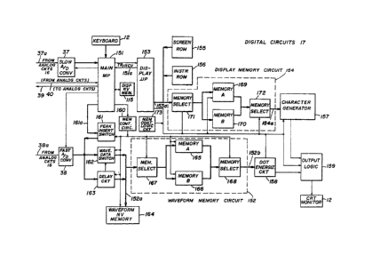
ReE~rrin~ to FIG. 16, the digital circuits 17
include a rnain rnicroprocessor lSl, a wave~orm memory
circuit 152, a display microprocessor 153, a display memory
circ~it 154, screen ROM 155 and instruction ROI~ 156. The
digital circuits further include a character generator
157, a dot energizing circuit 158 and output logic 159.
The main microprocessor 151 and the display microprocessor
153 also have associated memory control circuits 160 and
173, respectively.
~ he main microprocessor communicates directly
with the analog circuits 1~ (F~5. 15) via control line
39. Signal inputs to the digital circuits 17 from the
analog circuits 16 are provided by conductor 37a t~hich
conducts slow A/D information, conductor 38a which conducts
the fast A/D information and via signal conductors 40.
The main microprocessor 151 also communicates
directly with the display microprocessor 153 via serial
data transmit/receive lines 151a and receives and stores
KV peak values for each cylinder and supplies these values
to the ~7aveform memory circuit 152 via peak insert switch
161 at the appropriate time.
Peak Insertion
Digressing, the firing line on the ignition
signal, on the primary or on the secondary, has an
extremely rapid rise time as can be seen in FIGS. 4 and
6. ~either the fast analog to digital converter 38 nor
the slow analog to digital converter 37 acts sufficiently
fast to insure that the peak of the firing line will occur
precisely at the data point. ~7ithout additional circuitry,
the peak of the firing line on -the CRT screen would be
likely to be less, and perhaps substantially less, than
the actual peak value.
The present application discloses a circui~ for
detecting the peak of the firing line and causing such
peak to be displayed so that the ignition waveform on the
CRT screen does, indeed, accura~ely reflect its peak.
~ hen either the Primary or Secondary Pattern
mode is selected, t~e main microprocessor 151 instructs
the analog waveEorm processing circuit 3~ (F~G. 15) to
sample the waveform and capture the full height of the
'
firing line for each cylinder, providing a signal
representing the firing line peak value. At the correct
time, this information provided by the slow A/D converter
37 is accessed and converted by the main microprocessor
and then inserted into the waveform information being sent
to the waveform memory circuit ]52 by the fast A/D
converter 38 so that the full value of the firing peak
for any cylinder firing will be displayed on the CRT
screen.
Fast A/D converter 38 supplies in~ormation
directly to the waveform memory circuit 152 via a data
switch 162 or delay circuit 163. Non-volatile data storage
is provided by non-volatile display memory 115 and
non-volatile waveform memory 164.
There are two general classifications of data
that are processed. One is waveform data, such as the
digital data representing the primary and secondary
waveforms which are constructed, temporarily stored in
the ~aveform memory circuit 152 and then extended to CR~'
monitor 11. The other type of data is alphanumeric address
data which is temporarily stored in display memory circuit
154 and which when applied to character generator 157
provides character data to the CRT monitor 11.
The waveform ~emory circuits 152 include
identical memory banks, memory-A 165 and memory-B 166.
A memory bank switching arrangement is employed~ Selection
of which memory is read into and which memory is read out
of is controlled by memory control circuits 160 which in
turn control memory select circuits 167 and 168.
Similarly, the display memory circuit 154,
associated with the display microprocessor 153, employs
a bank switching arrangement including memory-A 169,
memory-B 170 and associated memory select circuits 171
and 17~. ~ddress data for the character generator 157
which formats fi~ed screen patterns is stored in screen
ROM 155 and the instruction ROM 156, both of which RO~ls
are read out Yia display memory circuit 154. The accessing
of the screen ROM 155 and instruction ROM 156 as well as
the addressing of the display memory circuit 154 is
controlled by the display microprocessor 153 via memory
control circuits 173. ~he address data read out of display
memory circuit 154 is extended to the character generator
157 which supplies appropriate digital signals representing
alphanumeric information to be displayed to output logic
159 whlch drives the CRT monitor 11.
The slow A/D information (as well as the Engine
Information such as number of cylinders and cycles, entered
by the user) is stored in the non-volatile display memory
115 under the control of the main microprocessor 151.
The slow A/D converter 37 handles information such as the
KV peak and battery voltage, and provides digital values
corresponding to the analog values of the signals. The
main microprocessor also receives inputs from the keyboard
12. The main microprocessor scans the ~eyboard 12, detects
any ~ey operation and effects the command or stores the
data represented by the keys operated. The main
micropLocessor sends d;gital information to the display
microprocessor via serial data transmit/receive lines 151a,
including mode identification signals derived from keyboard
operation.
r~aveform information is stored in the
non-volatile waveform memory circuit 164 under control
of the memory control circuits 160. The fast A~D converter
38 provides conversion of analog sisnals to digital signals
for primary and secondary signals, alternator diode pattern
signals and fuel injector signals and voltage pattern.
Due to the nature of the signals, the fast A/D converter
38 must have a very fast response time. Due to the fast
response time of the fast A/D converter 38, the ~ast A/D
converter 38 enters data directly into the waveform memory
circuit 152. In other words, the main microprocessor 151
does not take part in directing the fast A/D waveform data
to waveform m~mor~ circuit 15~. The fast A/D waveform
data is entered into memory-A 165 and mc~ory-B 166 through
hardware control by the memory control circuit 160 and
memory select circuits 167,168.
The main microprocessor operates under the
control oE programs stored in its ROM to receive and
process the slower information such as the pulses ~1 SYNC-X
and SYNC-X from which it derives synchronization. The
main microprocessor responds to the SYNC-X pulses, computes
RPM and generates a VCO signal based on engine RPM which
is used to correlate the sampling rate with engine speed
for the fast A/D converter 38 and storage of wa~eform data
in waveform memory circuit 152 and non-volatile waveform
memory 164.
There are two ways waveform data can be entered
into the waveform memory circuit 152 from the fast A/D
converter 38. One is from the fast A/D converter 38
through data switch 162~ The other way is through delay
circuit 163. The delay circuit 163 digitally delays the
digital data to effectively shift the displayed waveform
to the right (see FIG. 5) on the CRT screen to facilitate
analysis of the leading edge of the ~7aveform. In an actual
embodiment, the delay furnished by the delay circuit 163
~as fixed at 128 bytes. Since the extent of the CRT screen
was 512 bytes, the waveform on the CRT screen is moved
to the right approximately 25~ of the screen width. If
the waveform from the fast A/D converter 38 passes through
the data switch 162, the leading edge of the wavef~rm under
analysis is at the left-hand mar~in of the screen.
The non-volatile waveform memory 164 also shares
the data bus 152a. When enabled, incoming data is stored
in the non-volatile waveform memory 164 which can store
waveform data for up to eight cylinder firings. However,
the non-volatile waveform memory 16~ can only store at
one time, the data for the primary or the secondary
waveforms for all eight cylinders, or the fuel injector
wave~orms or the alternator diode or voltage patterns.
The peak value which is determined by the peak detector
circuit 120 ~FXG~ lS) is received and stored by the main
microprocessor 151 and eventually is supplied to data bus
. .
' ~ . ' ' . :
-37-
152a for application to the inputs of the delay circuit
163 and the waveform data switch 162, one of which is
enabled to pass the peak value data of all the waveforms
to the appropriate memory bank at the proper time.
In summary, for waveform data, the waveform
memory circuit 152 receives waveform data from the fast
A/D converter 38 (or peak insert data from the main
microprocessor via peak insert switch 161) via waveform
data switch 162, or the delay circuit 163, or data stored
in the non-volatile waveform memory 164. The source of
data is selected by the memory select circuit 167 under
the control of the memory control circuits 160.
A memory bank switching arrangement is employed
in passing waveform from the selected input source to the
CRT monitor 11 (FIG. 2). ~Semory select circuits 167 and
168 are operable in complementary fashion, allowing data
to be read into one of the memories, such as memory 165
while data is being read out of the other memory 166.
When data has been received for the selected waverorm,
the memory control circuits 160 switches the functions
of memory 165 and memory 166 such that data is read out
of memory 165 while incoming data is read into memory 1~6.
Data stored in non-volatile display memory llS representing
calculations such as RPM, Dwell, etc. made by the main
microprocessor, is passed to the display microprocessor
153 via data serial transmit/receive lines lSla.
The information read out of wavefor~ memory
circuit lS2 passes to dot energizing circuit 158 which
controls turn-on of the electron beam for the CRT monitor
11. The function of the dot energizing circuit is to
provide a more continuous waveform by filling in the dots
in the column of the one of two adjacent points located
in diferent row~, as in rising or falling waveforms.
With this arr~ngement, only 512 bytes are re~uired to
address the portion o~ the screen on which the waveform
is displayed. The dot energizing circuit 158 eliminates
the need ~or memory mapping or bit mappin~ to the screen.
~2763~3~
The OUtp~1t of ~he38dot energizing circuit 158
is extended ~o output logic 159 which also receives data
from the display memory circuit 154 and forms a composite
signal of waveform and display format data and drives the
CRT monitor 11 (FIG. 2).
The display data is handled in a similar manner
as far as memory is concerned. A bank switching
arrangement is employed. The display microprocessor 153
indirectly controls through memory select circuits 171
and 172, into which of the memories 169 or 170 data is
written to while data is being read out of the other
memory. ~he display microprocessor 153 uses the input
data bus 153a for transferring address data bet~een the
screen ROM 155 and the instruction RO~I 156 and the display
memory circuit 154 and uses output data bus 154a for
transferring address data from the display memory circuit
154 and the output logic circuit 159. The screen ROM 155
stores address data for application to the character
generator 1S7 to format the various screen patterns. The
instruction ROM 156 stores address data for application
to the character generator 157 to format instruction
screens which display information in text form such as
how to use the digital engine analyzer 10 (FIG. 1). The
display microprocessor 153 on demand from the control
signals provided by the main microprocessor 151 in response
to keyboar~ entry, accesses either the instruction ROM
156 or the screen ROM 155 to read out the appropriate
information which is passed via data bus 153a to the
display memory circuit 154. The display microprocessor
153 also does some calculation of data, particularly
conversion of data such as RPM value from hex code to
decimal format and passes this data via data bus lS3a to
the display memory circuit 154. The display microprocessor
also converts decimal values to ASCII or the code necessary
for use in character ~eneration.
Switching oE memories 169 and 170 between read
and write modes is controlled by memory select circuits
171 and 172 which receive control signals and address
.
- .
i3~
--3g--
information from the display microprocessor 153 via memory
control circuits 173. The output of display memory circuit
154 is extended to the character generator 157 which
responds to the addresses supplied thereto to output the
appropriate character data through the output logic 159
for application to the CRT monitor 11 (FIG. 2).
Detailed Digital System
FIGS. 17-24, when arranged as shown in FIG. 45,
illustrate a detailed block diagram or the circuits of
the digital circuits. Referring first to FIGS. 17 and
19, the main microprocessor 151 has an associated port
expander 201 including port expander circuits 201a and
201b ~7hich are used to expand the output capability of
the main microprocessor via a data and control bus 203
to which are connected inputs of the port expander 201,
inputs and outputs of the non-volatile display me~nory 115
(FIG~ 16), and the output of the slow A/D converter 37
(FIG. 16) and keyboard bus switch 202.
The main microprocessor receives input signals
~1 SYNC-X, DWELL-X, and SYNC-X from the analog signal
processing circuit 31 (FIG~ 15) and the STATUS signal from
the slow A/D converter 37. The main microprocessor
provides control signals RUN, LB-X, HB-X for the slow A/D
converter 37, analog circuit control signals SHORT-X and
PEAK/HOLD for the appropriate circuits, port expander
select sig nals I/O 1, I/O 2, WR-X, RD-X, and control
signals FREEZE, LATCH CONTROL, WRITE-X, S~ROBE-X,
NON-VOLATILE and HANDSHAKE for the memory control circuit
160, as well as RESET and KBD-ENABLE-X for the keyboard
bus switch 202 and transmit and receive serial data for
the display microprocessor 153.
The port expander 201 outputs main microprocessor
siynals PRI/SEC-X~ CYL IDO, CYL IDl, CYL lD2, FREEZE CLK,
SW ITCH CONTROL 0 and SW ITCH CONTROL 1 and data words COL
ON, COL OFF, PEAK DATA and VCO.
The k~yboard 12 has an associated keyboard bus
switch 2û2! which interfaces the key~oard 12 with the main
microprocessor via bus 203.. The main microprocessor
~L~f;i~
continuously scans the rows of the keyboard and column
information as sent to the main microprocessor via keyboard
bus switch 202 to enable determination of change in
function of any of the switches.
The keyboard is divided into rows and columns.
The main microprocessor scans the keyboard monitoring what
row it is in and looking for column information. When
a key is depressed, the corresponding column line becomes
low. The main microprocessor determines wllich column is
low and applies the algorithm for that row and column
entry. ~his is essentially a matrixing techni~ue, the
main microprocessor knowing the row and scanning the
columns.
Data Format
Referring to FIGS. 17 and 24, the main
microprocessor 151 communicates directly with the display
microprocessor 153 via serial data transmit/receive lines
151a. The information sent to the display microprocessor
153 via serial data transmit~'receive lines l51a includes
data such as the number of cylinders, the cylinder firing
order, measured data or data calculated by the main
microprocessor 151, such as engine RPM, voltage, KV values,
average dwell, etc., control information indicating that
a mode or feature is being activated or deactivated, and
mode words which identify each of operating modes and
features. Each set of data sent to the display
microprocessor 153 by the main microprocessor 151 is
preceded by a mode identifier word. In accordance with
a "handshake" arrangement, the displa~ microprocessor 153
upon receipt of data from the main microprocessor 151 sends
back to the main microprocessor the mode identifier word
to indicate that the data transmitted by the main
microprocessor has been received.
In the present illustration, the operating modes
and features are assigned the following mode identifiers:
.
.
-41-
Decimal Hex ~Sode/Feature
O 00 Start-up Screen
1 01 ~o. of Cylinders
2 02 No. of Cycles
3 03 Firing Order
4 04 Select Function
05 Primary Mode
6 06 Secondary Mode
7 07 Alternator Mode
8 08 Voltage Mode
9 09 Fuel Injector llode
OA Cylinder Shorting Bar Graph Mode
11 OB Dwell Bar Graph Mode
12 OC KV Bar Graph ~50de
13 OD AlternatorJFuel Question
14 OE Instructions Mode
OF not used
16 10 not used
17 11 Shorting Feature
18 12 Freeze Feature
19 13 RPM Setpoint Feature
14 Cylinder Selected
21 15 Memory Feature
VCO Clock Generator
-
The main rnicroprocessor also responds to the
signal SY~C-X to generate a VCO data word related to engine
speed in units of time. The main microprocessor includes
internal timers, hereinafter referred to as timer O and
timer 1, which are enabled to count at the rate of 1 pulse
per microsecond for time durations determined by the pulse
SYNC-X, for determining VCO rate and RPM rate. The RPM
and VCO rates are calculated under software control as
will be described with reference to the RPM calculation
subroutine, the flow chart for which is illustrated in
FIG~ 41C, and the VCO calculation subroutine, the flow
chart for which is illustrated in FIG. ~lD.
The rnain rnicroprocessor outputs a VCO data word,
via the port expander 201a, which is extended to a VCO
. ,
--42--
clock generator 204 (FIG. 18) of the memory control
circuits 160 ~FIG. 16). Referrring to FIG. 18D, the VCO
clock generator 204 comprises a digital/analog converter
205, an amplifier 206, voltage to frequency converter 207,
a VCO clock gate 207a and a pair of monostable circuits
208 arld 208a.
The digital/analog converter converts the VCO
data word to an analog voltage which is amplified by
amplifier 206 and applied to the voltage to frequency
converter 207 which, through VCO cloclc gate 207a, outputs
a VCO clock signal which varies in frequency from
approximately 0 Hz to approximately 250 RHz.
The VCO clock gate AND's the VCO clock signal
with a signal FREEZE-X output by the non-volatile waveform
memory 164 (FIG. 16). When the Freeze/i~emory feature is
activated, the main microprocessor sets the FREEZE line
high and sets LATCH CONTROL high which latches a flip flop
in the miscellaneous control logic 215 ~FIG. 18) . This
sets high signal FRE:EZE LATCH which is applied to the
non-volatile waveform memory 164 and inverted to become
FREEZE-X (FIG. 20) . The VCO clock signal is ORId with
a signal FREEZE CLOCK, a 125 KHz rate signal generated
by the main microprocessor as a fixed rate clock pulse
which is used whenever the Freeze/Memory feature is
active. The VCO clock signal or FREEZE CLOCK signàl,
depending upon whether or not the Freeze feature is active,
clocks monostable circuit 208 which in turn clocks
monostable circuit 208a. The monostable circuit 208
generates write signal WR/RDY which is applied to the fast
A/D converter 38 causing it to sample at the VCO clock
rate. ~onostable circuit 208a generates a signal MEM WRITE
which is used by the memory control circuits 160. Two
monostable circuits 208 and 208a are employed because
different pulse widths are required for the two signals
WR/RDY and MEM WP~ITE.
Re~erring to FIG. 19, the fast A/D converter
38 ~amples the analog signals supplied to the analog input
at a rate determined by the VCO clock signal or FREEZE
- - , '
.
~7~
-43-
clock when Freeze feature Is activated. The digital output
of the fast A/D converter 38 is applied to data bus 152b
and ultimately ex.ended to waveEorm memory circuit 152
(FIG. 20) and non-volatile waveEorm memory 164 (FIG. 20)
by waveform data switch 162 or delay circuit 163.
The slow A/D converter 37 under the control of
the main microprocessor 151 receives slow time varying
signals including peak data and voltage at its analog
input. The slow A/D converter 37 converts signals supplied
to its analog input when its input RUN is set high by the
main microprocessor 151. T~hen a conversion has been
completed the slow A/D converter 37 sets its STATUS output
high~ The STATUS output is read by the main microprocessor
151 under software control. The main microprocessor then
loads the data provided by the slow A/D converter 37 into
temporary registers in the main microprocessor for use
in calculations. Data obtained from the result of such
calculations is passed on to the display ~icroprocessor.
Peak data obtained from the slow A/D converter 37 is stored
in internal registers of the main microprocessor, a
separate register being provided for each cylinder, and
that information is transferred to port expander 201b
(FIG. 17) at the appropriate time and ultimately extended
to data bus 152b via peak insert switch 161 under control
of the main microprocessor 151 and the pea~ control logic
216 (FIG. 18).
Selection of data source, that is waveEorm data
switch 162, delay circuit 163, or the non-volatile waveform
memory 164 is controlled by the memory control circuits
160 (FIG. 20)~
Gates 163a and 163b associated with delay circuit
163 pass the signals NO~AL-TRIG and PRE-TRIG respectively
to the delay circuit 163 and waveform data switch 16~.
These are complementary outputs and are produced by the
miscellaneous control logic 215 (FIG. 18) in conjunction
with the main microprocessor 151. When NORMAL~TRIG is
selected, the main microprocessor 151 sets the CYL IDO
line low via the port expander 201b and momentarily togyles
,~
.
_d~4 _
the latch control line high. This causes the NOR~IAL-TRIG
output of the miscellaneous CONTROL LOGIC to be latched
low and the PRE-TRIG output to be latched high. In this
case I NORMAL-TRIG enables the waveform data switch 162
and PRE-TRIG disables the delay circuit 163.
Wh e n P R ~ ~ T R I G i s s e 1 e c t e d, t h e m a i n
microprocessor 151 sets the CYL IDO line high via the port
expander 201b and moznentarily toggles the latch control
line high. This causes the NORMAL-TRIG output of the
miscellaneous CONTROL LOGIC to be latched high and the
PRE-TRIG output to be latched low. In this case,
NORMAL-TRIG disables the waveform data switch 162 and
PRE-TRIG enables the delay circuit 163.
The signal FREEZE LATCHED is extended through
gates 163a and 163b to inhibit both the waveform data
switch and the delay circuit when the Freeze feature is
active. ~aveform data normally passes through the ~aveform
data switch 162 from the fast A/D converter 3B to ~ ave~orm
memory circuit 152 (FIG. 20) . ~aveform data is also
~ritten into non-volatile waveform memory 164 (FIG. 20)
which is controlled and addressed by memory control
circuits 160 (FIG. 18) to be written into ~hen FREEZE or
MEMORY features are inactive and to be read from when
FREEZE or MEMORY features are active. I~aveform data from
the fast A/D converter 38 passes through the delay circuit
163, when the ~aveform data swi tch 162 is inhibited, and
FUEL INJECTOR mode or PRE-TRIGGER features are selected~
In an actual ernbodiment, the main microprocesso~
151 was the INTE~ type 8051, the port expanders 201a and
201b were the INTEL type 8155 s_atic MOS RAM, the slow
A/D converter was the INTERSIL type 7109 12 bit binary
A/D converter, the fast A/D converter 38 was the National
Sem i cond uc tor Type 0 8 2 0 8-b i t h i gh spe ed compat ible A/D
converter, the digital/analog converter 205 was the
National Semiconductor type DAC 1220 and the
voltage/~requency converter was the Type 4153
voltage-to-~requency converter available fro~ Raytheon. The
delay circuit 163 was Zilog type 8060 buffer unit and FIFO
~3~3
expande~, the peak insert s5witch 161 and waveform data
switch 162 were the TI Type 74HCT245 Octal Bus
transceiver. The non-volatile waveform memory 164 was
the RCA/ type 6116 CMOS 2048 x 8 bit static memory and the
display non-volatile memory 115 was the Type 6561 256 x
4 CMOS RAM available from Harris Semiconductor.
~aveform llemory and Memory Control Circuit
Referring to FIGS. 18 and 20, the memory control
circuits 160 include A/D address system 212, memory bank
switch control logic 213, non-volatile memory logic 214,
miscellaneous control logic 215 and peak control logic
216. The memory select circuit 167 includes A/D address
switch 217, CRT address switch 218, A/D address switch
219 CRT address switch 220, and data switches 221 and 223.
The memory select circuit 168 includes data output switch
222 and data output switch 224.
As indicated, a bank switching arrangement is
employed in which data is written into one memory such
as memory 165 while data is being read out of the other
memory 166. Then the memory configurations are switched
and data is read out of memory 165 while data is written
into the other memory 166.
The two-memory-bank sys~em enables data to be
read into one waveform memory circuits at the slow rate
at which it is generated and at the same time read out
to enable data previously obtained and stored in the other
waveform memory circuit at the high rate required to
display the waveform data on the CRT screen without
flicker. If a new ~rame is created less frequently than
thirty times per second, the screen flickers. Sixty times
per second yields more favorable results. There are
131,072 intersections on the screen (512 X 256) which when
multiplied by 60 (screens per second) is 7.8 MHz. Thus,
an 8 MHz sweep rate is selected.
The rate at which data is delivered to the
waveforJn memo~y circuit varies with engine speed. The
rate at which data can be accepted ~rom the viewpoints
of sampling and addressing is in the range of 0 to 250
. .
KT~z, for a four cylinder engine. I'he latter value
corresponds to an engine speed of 14,648 rpm for 512
samples per waveform. At the maximum engine speed, data
is being read out of the waveform memory circuit 152 at
a rate 32 times faster than it is being delivered to the
wavefrom nemory circuit (8 MHz/250 KHz). At 1,000 rpm,
data is being read out of the waveform memory circuit
almost 500 times faster than it is being delivered to the
CRT screen.
Thus, the dual memory bank system enables data
to be read from one memory fast even though it is being
delivered to the other memory slowly. Of course, ,he data
for each frame will not be new. In fact, it will be the
same for at least 32 screens at the highest engine speed
and almost 500 frames at 1,000 rpm.
A/D address switches 217 and 219 pass write
addresses to the memory 165 and memory 166, respectively
and CRT address switches 218 and 220 pass read addresses
to the memory 165 and memory 166, respectively. Similarly,
data switches 221 and 223 extend waveform data from data
blls 152a to the memory 165 and memory 166, respectively
and the associated memory is configured for a write
operation. Data switches 222 and 224 pass data read out
of memory 165 and memory 166, respectively, to the output
waveform data bus 152b.
~ Semory 165 and memory 166 are selected by the
memory control circuits 160 (FIG. 18) which enable A/D
address switch 217 and data switch 221 to provide addresses
through A/D address switch 217 for storing waveEorm data
provided to the memory 165 through data switch 221 while
CRT address switch 220 is enabled to supply addresses to
memory 166 read out data through data switch 224 to the
output waveform data bus 152b.
After a block of data from a current sampling
interval has been stored in memory 165, such data block
be ng the 512 bytes representing a primary signal,
secondary signal I or other waveform information, the
waveform memory configuration is switched under the control
--47--
of the memory control circuits 160 (FIG. 18). Accordingly,
A/D address switch 217 and data switch 221 will be disabled
and CRT address switch 218 will be enabled to provide
addresses to memory 165 to read out data to the output
waveform data hus 152b through data switch 222 which is
also enabled. CRT address switch 220 and data switch 224
will be disabled and A/D switch 219 and data switch 223
will enable the waveform data from the next sampling
interval to be written into memory 166.
Thus, the switches 217-224 provide hardware
switching of address lines and data input lines and data
output lines, allowing data from one of the data sources,
wave~orm data switch 162 (FIG. 19), delay circuit 163
(FIG. 19) or non-volatile waverorm memory 164 (FIG. 19)
provided on data bus 152a to be read into one of the
memories such as memory 165 while data previously read
into memory 166 is being read to the CRT monitor.
The data supplied to the ~1aveform memory circuit
152 is a number representing the vertical height of a
particular point on the waveform to be displayed on the
screen. Ihe waveform is represented by 512 bytes, each
byte addressing a successive column of the CRT screen and
the magnitude coded by that byte corresponding to the row
of the screen. The information displayed is the waveform
for the cylinder selected. In other words, the waveform
for only one cylinder can be displayed at a time. ~'aveform
data for all cylinders, 512 bytes per cylinder, for the
selected screen, such as primary pattern screen, is stored
in the non-volatile waveform memory 164 (FIG. 16). ~hen
Freeze or Memory feature is activated, the data for the
selected cylinder is read out o~ the non-volatile waveform
memory 164 (FIG. 16) to the wave~orm memory circuit 152
for display on the CRT monitor.
As indicated, data is written into the waveform
memory circuit 152 at a ~irst rate and read out of the
wa~re~orm memory circuit 152 at a second rate. The input
addressing rate is a variable rate dependent upon the
frequency of ~he VCO clock signal which is established
7~3~
-48-
by the VCO clock generator 204 (FIG. 18) and which
establishes the sampling rate for the fast A/D converter.
Thus, waveform data being received by the digital circuits
is written into the waveform memory circuit 152 at a rate
corresponding to the sampling rate of the fast A/D
converter.
The data is read out of the waveform memory
circuit 152 at a rate of 15,750 Hz, the horizontal scan
rate for the CRT address counter 159 (FIG. 21) which also
controls the s~eep rate for the CRT monitor 11 (FIG. 2).
It is pointed out, that when the Freeze or ~lemory features
are active, data is read into the waveform memory circuit
152 at the rate of the 125 KHz freeze clock which is
generated by the main microprocessor.
In an actual embodiment, the address and data
switches 217-224 were the Type 74HCT245 TI Octal Bus
Transceiver, supplemented by an additional address switch,
such as the TYPE 7425244, and the mem~o ~ 165 and memory
166 each comprised two Type 2149H2 INTEL 1024x 4-bit ROM.
Memory Control Circuits
The memory control circuits 160 (FIG. 18), which
include A/D address system 212, memory bank switeh control
logie 213, non-volatile memory logie 214, miseellaneous
control logic 215 and peak control log;e 216, will now
be described.
Referring to FIG. 18A, the A/D address system
212 includes A/D address eounter 225, latch 225a, VCO cloek
gate 226, hardware cylinder counter 227, and ~/D address
counter reset circuit ineluding syne gates 22~-230, gate
231, freeze gate 232, divider cireuit 233 and A/D address
eounter reset circuit 234~ The A/D address counter.225
reeeives gated VCO clock pulses through VCO clock gate
226 and defines 512 addresses for the waveform memory over
output address bus 211a~ The reset circuit 234 resets
the A/D address counter in response to each SYNC pulse.
The reset pulse is gated with the VCO clock signal for
~ynchronization purposes~
,.
.. , ' . :
,-
,
~3`~3~
The hardware cylinder counter 227 is driven by
successive SYNC pulses provided (as reset pulses) to count
up fr~m 0 providing an indication of the cylinder which
iS flrlng.
The SYNC pulses are normally passed to the reset
circuit 234 (and to the hardware cylinder counter 227~
through gate 228, gate 231 and freeze gate 232 which passes
SYNC pulses to A/D address counter reset circuit 234 only
~hen Freeze Feature is not active.
When the Fuel Injector mode is active, gate 228
is inhibited by signal FUEL-X and gate 229 is enabled.
The SYNC pulses are divided by the divider circuit 233
which performs a divide-by-4 circuit operation resulting
in one reset signal being passed through gate 229, gate
231 and FREEzE gate 232 to the A/D counter reset circuit
234 for each four fuel injector pulses.
Gate 230 prevents resetting of the A/D address
counter 225 by SYNC pulses when the Freeze mode is active.
In Freeze mode, the A/D address counter 225 counts
continuously.
Referring to FIG~ 18, the miscellaneous control
logic 215 comprises three data latches 215a-215b and 215c
having their data inputs connected outputs FREEZE mode,
CYL ID0 and CYL IDl, respectively, of the main
microprocessor (signals CYL ID0-IDl being passed via ~ort
expander 201b), and their clock input connected to a LATCH
CONTROL signal output of the main microprocessor. The
data latches 215a-215c are used to generate output signals
FREEZE LATCHED, NORMAL TRIG and PRE-TRIG, and FUEL and
FUEL-X, respectively.
The signal FREEZE LATCHED is generated when the
Freeze mode is entered. Signal NOR~AL TRIG is normally
high, but latch 215b is reset to set signal PRE-TRIG high
when the Special Trigger ~eature is enabled. Signal FUEL
is set high when F~el Injector mode is selected. The main
microprocessor outputs signals over the lines FREEZE,
cylinder ID0 and cylinder IDi, for only a short time during
an operating cycle, and generates a write command to latch
~ . .. ___ . , _ _ . ._ ,. ., . . _ _ . _ , ,~ . . ,,, _ . _ ._
', ~ , , ' .
.
-50-
these signals into the data latches 215a-215c when the
appropriate commands are generatedv
Referring to FIG. 18Br the memory bank switch
control logic 213 includes a cylinder comparator circuit
236, address and data switch logic 237 and memory enable
and write logic 238. The cylinder comparator circuit 236
compares the outputs of the hardware cylinder counter 227
(FIG. 18A) with the cylinder identification received over
lines ID0-ID2 from the main microprocessor. The main
microproce~sor ID lines ID0-ID2 and the outputs of the
hardware cylinder counter 227 (FIG. 18A) identify cylinders
as numbers 0-7, with the 0 being significant. Therefore,
cylinder number 1 is identified as 0 on the lines ID0-ID2
and hardware cylinder outputs ADDR9-ADDRll, cylinder 2
as 1, etc. The output of the cylinder comparator circuit
236 goes high when the hardware cylinder counter 227
reaches the count of the selected cylinder as indicated
by the cylinder ID lines ID0-ID2. The address and data
switch logic 237 receives the cylinder compare pulse and
switches the state of memory bank select signals .~5A and
MB with the falling edge of the cylinder co~pare pulse.
The memory enable and write logic 238 inclu~es
~ND gate 238a, AND gates 238b, 238c and A~D gates 23~d,
238e. In the memory enable and write logic 238, gate 238a
AND's the cylinder compare pulse with the gated memory
write pulse ~EM WRITE provided by non-volatile memory logic
214 (FIG. 18D) and gates 238b and 238c combine the
resulting signal with the memory select signals MA and
~B to generate write enable signals WRA, WRB, Signals
WRA and ~RB are combined by gates 23~d and 238e with
signals MA and MB to provide select signals CSl, CS2 for
the memory 165 and memory 166 (FIG~ 20), respectively.
Still referring to FIG. 18B, the non-volatile
memory logic 214 comprises gate circuit 235 which passes
signal MEM WRITE, generated by the VCO clock generator
when a slgnal counter CTR ~OLD OFF-X, provided by the A/D
address system 212 ~FIG. 18), is high~ The signal ME~
WRITE is combined with the signal FREEZE-X by gate 235a
~ ~o~$~
(not shown) to generate si~nal FREEZ~-X and MEM WRITE which
control activation o~ the non-volatile memory 164 (FIG. 20)
when FREEZE mode is active.
Waveform data for each cylinder (including peak
values) which are passed through the waveform data switch
162 (FIG. 19) (or delay circuit 163) are written into the
non-volatile display memory 164 under the control of the
address system 212 (FIG. 18). The hardware cylinder
counter outputs are the high order address lines of the
non-volatile waveform memory 164. The waveform data are
being stored in the non-volatile waveform memory 164 in
increments of 512 bytes per cylinder. Therefore, the
non-volatile waveform memory 164 stores up to eight 512
bytes of waveform data. When Freeze or Memory feature
is activated, the waveform data stored in the non-volatile
waveform memory is read out of the non-volatile waveform
memory 164 to the waveform memory circuit 152 unde~ the
control of the A/D address system 212.
Operation of Waveform and Memory Control Circuits
Referring to FIGS. 18 and 20, for purposes of
illustration of the operation of the waveform memory
circuit 152 and memory control circuits 160, it is assumed
that the Primary Pattern mode is selected and that the
main microprocessor has sent suitable control signals to
the analog circuits 16 (FIG. 15) to initialize the analog
circuits The control signals generated by the main
microprocessor for the Primary Pattern mode initialization
of the analog circuits include signals SWITCH CONTROL 0
at logic high, SWITCH CONTROL 1 at logic low, and
PRIM/SEC-X high. These conditions for these signals select
the primary signal and the primary sync. The control of
the slow A/D converter 37 (FIG. 19) and the fast A/D
converter 38 (FIG. 19) will be described in the next
section entitled Peak Insertion, and the instant
description will be limited to the addressing and loading
oE ~he ~avçEorm memory circuit 152 ~or the condition where
Primary ~attern mode is selected.
y~
-52-
I'he main microprocessor will respond to the pulse
SYNC-X and #l SYNC-X to calculate VCO and RPM values as
described more ~ully in the sections entitled VCO
Calculation and RP~ Calculation. The main microprocessor
sets cylinder ID lines ID0-ID2 to identify the cylinder
for which the waveform will be displayed on the CRT
monitor. In the present example, it is assumed that the
third cylinder has been selected and accordingly the binary
coding for 2 (starting from 0, with zero significant) is
set on cylinder ID lines ID0-ID2. This information via
port expander 201b is extended to the cylinder comparator
circuit 236 (FIG. 18B) . A gated VCO clock generated by
the VCO cloc~ generator is extended to the address counter
225 tFIG. 18A) . The VCO clock rate is calculated by the
main microprocessor in correspondence to the RPM rate for
engine speed such that there will be approximately 512
VCO clock pulses for every cylinder firing. These address
pulses are applied via A/D address lines 211a to the
non-volatile waveform memory 164 (FIG. 20) and to the
inputs of the A/D address switch 217 and A/D address switch
219 associated with memory 165 and memory 166,
respectively.
Referring to FIG. 20 and to the timing diagram
shown in FIG. 18C, it is assumed initially that signal
MAf FIG. 18C, line G is set high and signal MB, FIG. 18C,
line H is set low, si~nal CSl, FIG. 18C, line I is set
high and signal CS2, FIG. 18C, line J is set low. Under
these conditions, memory 165 is selected to be read from
and memory 166 is selected to be written into during the
time the waveform signal for the selected cylinder,
cylinder 3, is being processed by the fast A/D converter.
Thus, address switch 219 is enabled to pass the write
pulses to the memor~ 166 and data switch 223 is enabled
to pass the prirnary signal wave~orm data on data bus 152a
to the memory 166 where it is stored in consecutive
locations in accordance with the address pulses applied
to memory 166 through address switch 219. Also, CRT
address switch 218 i5 enabled to pass CRT address to memory
',
.
~71$:3~
-53-
165 with data switch 222 being enabled to pass the data
read out to the output waveform data bus 152b.
ReEerring to FIG. 18A, the SYNC-X pulses are
inverted by inverter 228a and passed through AND gate 228
(since signal FUFL-X is at logic high), and the SYNC pulses
pass through gate 231 and Freeze gate 232, since signal
FREEZE-X is a logic high level, to reset circuit 234.
The first SYNC pulse resets A/D address counter 225 which
then counts VCO clock pulses to generate 512 address pulses
for the memory 166. After 512 address pulses have been
generated, latch 225a is set by signal ADDR-X 8; setting
high the signal CO~NTER HOLD OFF. The SYNC pulse gated
by HANDSHAKE by gate 227a also resets the hardware cylinder
counter 227 to zero. The hardware cylinder counter 227
is then incremented each time a SYNC pulse is received
and counts up from 0-7 for an eight cylinder engine and
is then reset when the signal HANDSHA~E is sent by the
main microprocessor. The outputs ADRS 9-11 of the hardware
cylinder counter 227 are passed to the cylinder comparator
circuit 236 (FIG. 18B) and compared witll the state of the
cylinder ID lines IDO-ID2, which are set to a binary 2
code since the waveform for cylinder 3 is to be displayed.
Referring to FIG. 18B and the timing diagram
~'IG. 18C, the SYNC pulses, FIG. 18C, line A, generated
after the occurrence of the ~irst ~1 sync pulse shown at
260 in FIG. 18C, line N, increment the hardware cylinder
counter. The outputs, FIG. 18C, lines B-D on lines ADDR
9 - ADDR 11 represent the binary count (starting with zero)
for the number of SYNC pulses received. When three ~YNC
pulses are received, the binary count equals that for the
state of t~e cylinder ID lines IDO-ID2, and the output
oE the cylinder comparator circuit ~36 goes high (FIG. 18C)
line E. This causes the gated MEM WRITE signals to be
passed to the select input CSl and the write WRA of memory
165 to cause the waveEorm data for cylinder 2 being entered
onto the data input bus 152a, that is the waveform data
Eor cylin~er 3, to be written into the memory 165.
- : , : . .
-
.,
.
'
In response to the next SYNC pulse, cylinder
hardware counter 227 (FIG. 18A) is incremented causing
the output of the cylinder comparator circuit 236 to go
low (FIG. 18C, line E). This causes the address and data
switch logic 237 (FIG. 18B) to switch the states of signals
MA and MB (FIG. 18C, lines G and H). The memory enable
and write loyic 238 causes signal CSl to go to logic low
and signal CS2 to go to logic high (FIG. 18C, lines I and
J). With these conditions set, A/D address switch 217
is enabled to pass address pulses to memory 165 and data
switch 222 is enabled to gate waveform data from input
data bus 152a to memory 165. Also, CRT address switch
220 is enabled to gate CRT address pulses to memory 166
and data switch 224 is enabled to pass the data read out
o~ memory 166 to the output data bus 152b. Although the
read operation will start immediately, the write operation
will be delayed until the next time cylinder 3 is fired
as indicated by the output of the cylinder comparator
circuit 236 going to a logic high level. It should be
noted that the switching of memory 166 from write to read
condition and switching of memory 165 from a read to a
write condition is done under the control of hardware
circuits and is a function of the cylinder selected. Read
out of the data from the memory selected for a read
operation is controlled by the addressing circuits
associated with the display memory circuit 154, the data
being read out at the rate required for synchronization
with the CRT monitor, independently of the frequency of
the write operation. Although memory bank switching may
occur midway in a read cycle, corresponding memory
locations will be accessed in the memory being switched
from a write to a read operation so that the same memory
locations in the memory selected ~or read will be accessed
at the time of the rnemory bank switching operation.
Re~erring to FIGS. 18A and 18C, just beEore the
end o~ the ~iring period of the last cylinder, cylinder
3 in ~he present example, the main microprocessor sets
high the signa~ HANDSHAKE which is applied to gate 227a
'
_~,5_
at the reset input of the hàrdware cylincler counter (FIG.
18C, line M) . This output is ANDed with the next SYNC
pulse (FIG. 18C, line A) generating a clear pulse CLR
(FIG. 18C, line F) which resets the cylinder hardware
counter 227 to zero in preparation for the next cylinder
count operation.
Also, af ter 512 address pulses have been
generated, the output on address line ADDR-X 8 goes low
generating signal CTR HOLD OFF-X which is applied to gate
235 (FIG. 18B) as an inhibit signal to prevent the gated
MEM WRITE pulse from being passed to the memory enable
and the write logic 238 until the A/D address counter 225
is reset. The A/D counter reset circuit 234 is clocked
at the VCO clock rate to insure that the A/D counter 225
is not reset prematurely.
Peak Insertion
.
Referring to FIG. 15, when either the Primary
or Secondary Pattern mode is selected, the signal SWITCH
CONTROL 1, from port expander 201b (FIG. 17), on conductor
110a is at a logic low. For the Primary Pattern mode,
the signal SWITCH CONTROL 0, from port expander 201b, on
conductors 110b and 101a is at a logic high. For the
Secondary Pattern mode, such conductors are at a logic
low. A high logic level for signal SWITCH CONTROL 0 causes
the peak insert select circuit 101 to select the sync pulse
derived from the primary wave~orm, whereas the opposite
log ic level of signal SWITCH CONTROL 0 causes selection
of the sync pulse derived from the secondary waveform.
Signals SWI~CH CONTROL 0 and SWITCH CONTROL 1 control
multiplexer 110 to select which of the primary signal or
the secondary signal is passed to the slow A/D converter
37 and the fast A/D converter 38.
Assume, for example, that the Primary Pattern
mode îs selected. Then, the main microprocessor sets
signal PRIM/SEC-X high on conductor 86a high, thereby
causing sync select circuit 86 to select the primary
wave~orm as th~ source oE the signal sync . The primary
sync signal is passed to the peak in~sert select circuit
.' ' ' , . . ' . '
. . .
.. . . . .
': ', ' ' .:
.
'R~
-56-
101. For the Primary Pattern mode, signal SWITCH CONTROL
0 is set at loyic high, causing the peak select circuit
101 to pass the sync signal to its output as signal PEAR
INSERT.
The logic low level on conductor 110a and the
logic high level on conductor 110b causes multiplexer 110
to select the primary waveform, appearing at the output
of buffer 111, to be passed to the peak gate 119 and
through amplifier 112 to the fast A/D converter 38.
Multiplexer 110 also connects the output of the peak
detector circuit 120 to the input of the slow A/D converter
37.
The main microprocessor lSl operates under stored
program control to determine if the peak value for the
next cylinder in the firing order is to be inserted. If
so, signal PEAK/HOLD is set to a logic high, enabling the
peak gate 119 to gate the primary waveform to the peak
detector circuit 120. In that circuit, the peak value
of the primary sync pulse is determined and its value
stored. At the end o~ the firing period for the selected
cylinder, the main microprocessor sets signal PEAK/HOLD
low, disabling peak gate 119, and provides a logic high
at the RUN input of the slow A/D converter 37 (FI&. 19),
wh;ch had, until that event, been disabled.
The slow A/D converter 37 converts the peak value
stored by the peak detector circuit 120 to a two byte
digital word. ~1hen the conversion is complete, the STATUS
output (FIG. 19) of the slow A/D converter 37 is set high.
The converter 37 generates a signal CONVERSION COMPLETE
which is applied to the peak detector circuit 120 to reset
same.
Referring to FIGS. 17 and 19, when the output
STATUS of the slow A/D converter 37 becomes high, the main
microprocessor 151 sets the slow A/D converter RUN input
at logic low and enables outputs HB-X and LB-X, in
succession to read out the two bytes of peak value data~
The di~itaJ.ly coded peak value ~rom the converter 37 is
read into an internal register of the main microprocessor
-57-
dedicated to the selected cylinder. Other registers are
respectively dedicated to the other cylinders. The main
microprocessor keeps track of the cylinder count and
transfers the digital peak val~le data to port expander
201b where it is latched. The peak value latched in the
port expander 201b will be from either two or three
dlstributor revolutions previous to the present cylinder
firing, depending on the number of cylinders selected~
However, the peak data will be inserted as one byte into
the primary waveform data of the proper cylinder. Peak
value insertion is done under the control of the peak
control logic 216 shown in FIG. l9a.
The peak insert signal provided by peak insert
select circuit 101 (FIG. 15) is applied to the peak control
logic circuit 216 which generates two output signals PEAK
and PEAK ENABLE. Signal PEAK is coupled to the fast A/D
converter 38 to inhibit same for a one byte period. Signal
PEAK ENABLE is coupled to the peak insert switch 161 (FIG.
19) which gates the peak value data stored in the port
expander 201b to the waveform data bus 152b.
More specifically, the pealc control logic circuit
216 includes gates 331, 333 and 334 and a latch circuit
332. The signal PEAK INSERT is coupled to the signal input
of the gate 331, the control inputs of which are connected
to receive signals SWITCH CONTROL-X 1 and FUEL-X. Signal
SWITCH CONTROL-X 1 is high during the Voltage and
Alternator Modes and signal FUEL-X is high during the Fuel
Injector Mode. A high on either of the control inputs
disables the gate 331, while a low enables same. Signal
SWITCH CONTROL-Xl is low during the Primary and Secondary
Modes, so that the gate 331 is enabled while the analyzer
is in such modes, and the signal PEAK INSERT is stored
in the latch circuit 332.
The gate 333 has a signal input coupled to the
latch circuit 332, one control input to receive signal
A~D-X ~. Si~nal PEAK CLOC~ enables the gate after the
beginning o the operation of VCO, that is, with the start
of each 512 count cycle for the A/D address counter 225
--58--
(FIG. 18A) . Before that tirne, the gate 333 is disabled.
Signal ADRS-X ~ enables the gate 333 only during the first
half of the sweep, that is, up to count 256 and disables
the gate for the second half, that is, between COUIltS 256
and 512. In combination, therefore, the gate 333 is
enabled during the window of counts 0 to 256.
Gate 33~ has its signal input coupled to gate
333 and its control input coupled to receive signal
SHORT-X. During the Cylinder Shorting l~lode, the signal
on such control input disables gate 334. The output of
gate 334 in the signal PEAK SIG and its complement YEAK
ENABLE is generated by inverter 335 (not shown) .
Referring to FIG. 19, the signals PEAK ENABLE
and PEAK are generated from the present cylinder firing.
The signal PEAK ENABLE enables the peak insert tri-state
switch 161 to pass the peak information stored by port
expander 201b (FIG. 17) to the waveform data bus 152b.
At the same time signal PEAR is applied to the fast A/D
converter 38 to inhibit same for the duration of one VCO
clock pulse.
Freeze/Memory Feature
Referring to FIG. 20, the Freeze feature is
activated as a result of the operator depressing the freeze
key or the RPM set point being exceeded. The Memory
feature i5 activated upon entering a start-up screen mode
with waveform data saved in the non-volatile memory, or
in changing from a mode in a freeze state to a mode which
has waveform data saved in the non-volatile memory~ The
main microprocessor causes signal FREEZE to be latched
in data latch 215a of the miscellaneous control logic 215
tFIG. 18) . This signal is applied to the non-volatile
waveform memory 164, which configures same for read
operation, allowing waveform data previously written into
the non volatile waveform memory 164 to be read out of
it in response to address pulses supplied by the A/D
address generator 212 (FIG. 18). The signal FREEZE L~TCHEI~
is also appli~d ko the delay circuit 163 (FIG. 19) via
gate 163b, ~nhibiting that circuit. The signal FREEZE
. - - . . , :
~' , ~, . .
'
..
.~p~
-59-
LATCHED is applied to the waveform data switch 162 (FIG.
19) via gate 163a, terminating signal NORMAL ENABLE thereby
inhibiting the waveform data switch 162. Accordingly,
waveform data present on input data bus 152b from the
output of the A/D converter 38 is prevented from being
extended to the data bus 152a which now receives data from
the read out of the non-volatile waveform memory 164.
Writing of the in-formation read out of the
non-volatile me~ory 164 is controlled by the A/D address
system 212 (FIG. 18), including selection and memory bank
switching operations. However, the A/D address system
212 is clocked at the freeze clock rate rather than the
VCO clock rate and is prevented from responding to sync
pulses.
More specifically, with reference to FIG. 18DJ
signal FREEZE is applied to the VCO clock inhibit gate
207a, which is then prevented from passing the VCO clock
pulses. The FREEZE CLOCK pulses provided by the main
microprocessor at the 125 KHz rate trigger the monostable
circuits 208 and 208a of the VCO clock generator 204.
Referring now to FIG. 18A, the freeze clock
pulses are passed to the A/D address counter 225 for
incrementing the A/D address counter 225 at the fixed
freeze clock rate. The signal FREEZE inhibits the ~reeze
gate 232 to prevent sync pulses from being applied to the
hardware cylinder counter 227 or the to A/D address counter
reset circuit 23~. The A/D address counter address line
A~RS8-X iS gated with the signal FREEZE LATCHED and this
signal is applied to the hardware cylinder counter 227,
to increment the counter 227 at the end of each 512 byte
time interval, effectively replacing the SYNC signal which
normally increments the hardware cylinder counter.
When the Freeze eature is disabled, as by
selection of a different mode or subsequent operation of
the FREEZE key, the main microprocessor changes the state
o~ the signal FR~EZE LA~CHED in the data latch 215a (FIG.
18) which initializes the ~/~ address system 212, the
non-volatile memory 164 (FIG~ 20), waveform switch 162
.. . . . . .. . . . . . . . . . .. . .
'
~' ' ' ' ' ' '
.
(FIG. 19) and dela~ circuit ~3 (FIG. 19) to the operating
condition described previously.
Fuel Injector Mode
When operating in the Fuel Injector mode, at
least two complete injector pulses are displayed on the
screen at one time. Although approximately four fuel
injector pulses are usually displayed, the leading edge
of one of the pulses and the trailing edges of another
one of the pulses may be missing. The pattern can be
expanded for detailed viewing by activatin~ the ~aveform
Expansion feature and the pattern can be frozen by
activating the Freeze feature to permit the operator to
make a time measurement of fuel injector "on time" or any
other segment of the pattern.
The operation o~ the memory control circuits
160 (FIG~ 18) during Fuel Injector mode is similar to that
previously described for the Primary Pattern mode, and
the differences in operating modes is now described.
Referring first to FIG. 17, when Fuel Injector
mode is selected, the main microprocessor outputs switch
control data to port expander 2nlb setting signal SWITCH
CONTROL 0 and SWITCH CONTROL 1 to logic high levels. These
outputs are processed by fuel gain s~7itch logic 239 which
sets signal FUEL GAIN high. This signal is extended to
the analog circuits 16 (FIG. 15).
Referring to FIG. 15, the signal FUEL GAIN is
applied to the gain selector switch 113 which switches
a larger feedback resistor to the wave~orm amplifier 112.
~ s described previously, the fuel injector signal
applied to lead 22 passes through primary attenuator 84
and wave shaper 85 to sync select circuit 86 which is set
to pass the sync pulse derived from fuel injector pulses
through ~lanker cicuit 87 and inverter 88 as output
SYNC-X. Also, the ~uel injector signals are passed through
buffer 111 to the multiplexer 110 which is selected to
pass this input since signals SWITCH CONTROL 0 and SWITCH
CONTRO~ 1 ar~ hoth set to logic high levels. The output
o~ the multiplexer 110 is passed through wav~form amplifier
; . . ,, '
' ~ .
~27~
--61--
112 and via conductor 38a to the fast A/D converter 38
(FIG~ 17) .
Referring to FIGS~ 17-19, when Fuel Injector
mode is selected, the main microprocessor sets cylinder
ID line IDl (from port expander 201b) high, momentarily,
and latches this signal into the data latch 215c causing
signal FUEL to set at logic high level and its complement
FUEL-X is set at logic low level. These control signals
are applied to the A/D address system 212 (FIG. 18A) and
are used as gating signals to pass or block information.
When Fuel Injector mode is selected, the main
microprocessor also causes cylinder ID line ID0 (from port
expander 201b) to be set high and latches this input into
data latch 21~b which latches signal NORMAL TRIG high and
latches signal PRE-TRIG low. These signals are applied
to the delay circuit 163 to enable same and disable the
waveform data switch 162, as previously described for
Freeze feature, so that the fuel injector pulses provided
at the output of the fast A/D converter are extended via
data bus 152b through the delay circuit 163 to the waveEorm
data bus 152a.
Referring to FIG. 18A, the signal FUEL is applied
to the A/D address system 212 where it enables gate 229
to permit the A/D address counter 225 to be reset by
incom ing SYNC pulses . The signal FUEL-X inhibits gate
228 but the signal FUEL enables gate 229 to pass the
incoming SYNC pulses, which are divided by divide-by-four
circui~ 233, to the gate 231 and through freeze gate 232
to the A/D address counter reset circuit 23q. SYNC pulses
are divided by four to enabl~ up to four injector pulses
to be displayed on the screen of the CRT monitor at the
same time. The P./D address counter 225 receives only one
reset sync pulse for four fuel injector pulses.
Referring to FIG. 18B, the memory bank switch
control log ic 213 operates in the manner prev iGusly
described with respect to the Primary Pattern mode to
effect memory bank switching operatiQns, with the state
of signals MA and MB bein~ reversed Eor each eight fuel
injector pulses but with the select signals CSl/CS2-X,
and write signals WRA/WRB-X being generated for a tirne
corresponding to four fuel injector pulses to enable at
least to complete four injector pulses to be displayed.
In the next cycle, the complements of the select signals
and write pulses are generated for a period corresponding
to four fuel injector pulses.
Referring to FIG. 18A, the sync pulses derived
from the fuel injector pulses passed by gate 229, gate
231 and FREEZE gate 232 also increment the hardware
cylinder counter 227. As ind icated, because of the
divide-by-4 function of gate 231, when eight injector
pulses have occurred, only two count up pulses have
occurred. At such time, address line ADRS 10 of the
hardware cylinder counter 227 is set to logic high level
and this output enables gate 227c to reset the cylinder
hardware counter 227 to zero when signal FUEI. is high.
Referring to FIG. 18B, the cylinder comparator
circuit 236 provides a logic high level at its output
whenever the state of the cylinder counter 227 (FIG. 18A)
corresponds to the state of the cylinder ID lines IDO-ID2.
When Fuel In jector mode is selected, the main
microprocessor sets the cylinder ID lines IDO-ID2 low so
that the output of the cylinder comparator circuit 236
will be set to logic high whenever the hardware cylinder
counter 227 is cleared. This transition causes the signals
MA and l~iB to chan~e state e~fecting a memory bank switch
operation via address and data switch logic 237. Also,
memory enable and write logic 238 switches the state of
select lines CSl and CS2 to enable the appropriate switches
for routing the A/D address pulses and the waveform data
to the correct bank of memory when writing to memory and
similarly to turn on appropriate switches for routing CRT
address pulses and data to the CRT when reading from the
memory.
In summary~, A difEerent memory bank is written
to every eighth fuel injector pulse. Four fuel injector
pulses are written to mernory during each write phase.
--63--
Display Microprocessor and Syne Generator
Referring to FIGS. 21-24, the main microproeessor
151 sends mode select and function identifier words,
eentrol signals and numerieal data to the display
mieroprocessor 153 over serial transmit/receive lines
151a. The display microproeessor processes and generates
data to the display memory eircuit 154 and transfers data,
representing character address data, from the screen ROM
155 and/or the instruction ROM 156 to the display memory
cireuit 154 from which it is ultimately moved to the
charaeter generator 157 (FIG. 16).
For example, when the Primary Pattern mode is
seleeted, the display microproee ,sor causes the address
data representing the format for the Primary Pattern mode
sereen (FIG. 4) to be read into both memory 169 and memory
170.
A memory bank switchin~ arrangement, similar
to that for the waveform memory cireuit 152 (FIG. 20) is
used for the display memory circuit 154. However, the
display mieroprocessor 153 controls the memory bank
switching and memory bank switching is effeeted on the
basis of need to update the data being displayed, as when
updated data is received from the main mieroprocessor
rather than on a periodic basis. Note that the screen
format information is fixed and then once the sc~een format
information is written to both memory 169 and memory 170
from sereen ROM 155, this information need not be rewritten
until a new mode is seleeted. Variable information, sueh
as numerieal data values is stored in eorresponding
seetions of the memory 169 and the memory 170 dedieated
to variable data, and this data is updated on the sereen
as often as is neeessary under eontrol of the display
mieroproeessor.
Referring to FIG. 21, the syne generator 240
reeeives a master eloek signal at 2 MHz provided at the
QUtpUt of~ the master eloek and divider 240a whieh generates
an 8 MHz signal whieh is divided down to provide the 2
MHz signal for the syne generator 240.
4~
-64-
The sync generator 240 provides a composite sync,
a vertical drive signal and its complement at 60 Hz
horizontal drive signal and its complement at 15,750 Hz,
a composite sync, a gated composite sync, and a vertical
blanking signal.
In an actual embodiment, the display
microprocessor 153 was the INTEL Type 8051 the master clock
240 was the Intersil Type 720~ CMOS clock generator with
external frequency determining elements selected to provide
a 8 MHz clock signal, and including a divide by four stage
to provide the 2 MHz signal for the sync generator 240.
The sync generator was the Fairchild Semiconductor Type
3262A. The screen ROM and instruction ROM were the l'ypes
P2764 and P27128, respectively.
Display Memor~ Circuit
Referring to FIGS. 22 and 24, the display memory
circuit 154 is controlled in a manner similar to that for
the waveform memory circuit 152 (FIG. 20) with tri-state
address and data switches bein~ employed to enable
addressing of each memory selectively for read operations
via common address bus 250a and for write operations via
a common address bus 153b writing data provided on input
data bus 153a and reading out data to the CRT monitor via
output data bus 154a.
Thus, memory select circuit 171 includes
character address read switch 241 and character address
write switch 242 associated with memory 169, character
address read switch 243 and character address write switch
244 associated with memory 170 and data switches 246 and
~4~ which provlde paths for data written into memory 169
and memory 170, respectively.
Memory select circuit 172 includes data switch
245 which provides a path for data being read out of memory
169, and data switch 2~7 which provides a path for data
being read out oE memory 170.
Memory enabling and write signals Eor the two
memorie~ 16~ and 170 and associated address and data
switches are provided by the memory control circuit 173
3~
--65--
(FIG. 24) which outputs complementary select signals MAl
and MBl for the address and data switches 241-2~8 and
outputs complen~entary write signals WRAl-X and WRBl-X for
the memory 169 and memory 170, which enable one memor~
such as memory 169 to be written into while the other
memory 170 is being read from and vice versa.
Write addresses for the display memory circuit
154 are provided by the display microprocessor on address
bus 153bo Read addresses for memory 169 and memory 170
are generated by character read circuit 249 which includes
a di~7ide by seven counter 249a, a character column address
counter 249b and a character row counter 249c.
Referring to FIGS. 22, 2~ and 24A, the memory
control circuit 173 enables bank switching to occur only
during the vertical blanking period for the CRT monitor
to prevent the display of random data as may occur during
bank switching. The memory control circuit 173 (FIG. 24A)
includes latch 173a, latch 173b, yate circuit 173c and
gate circuit 173d. Latch 173b provides complementary
memory enabling signals MAl and MB1 which control enabling
of memory 169 and memory 170 and address and data switches
241-248 for read and write operations. Gates 173c and
173d, when enabled by the display microprocessor, pass
signals MAl and Msl, respectively, as write signals WRAl-X
and WRBl-X to the memories 169 and 170.
Referring to FIG. 22, when signal MAl is logic
high, memory 169 is selected to be read out, with address
switch 241 being enabled to pass read addresses to the
memory 169 and data switch 24S being enabled to pass the
data read out to the output data bus 154a. At the same
~ime, signal rssl enables memory 170 ~or a write operation.
Write address switch 244 and data switch 248 also being
enabled to supply addresses and data to the memory 170,
the data being written into the memory 170 in response
to the write signals WRAl-X. When latch 173b (FIG. 24A)
is to~gled, its outputs switch state and memory 169 is
selected Eor a write operation and memory 170 is enabled
-66-
to be read from, with address switches 242 and 243 and
data switches 2~6 and 247 being enabled.
Referring to FIGS. 24 and 24A, latch 173b is
switched in response to the vertical drive pulse whenever
the display microprocessor changes the state signal RD-X.
The use of the vertical drive pulse to switeh latch 173b
ensures that the bank switching will occur during the
vertical blanking period. To ensure that latch 173b has
been switched before activatin~ the memory write signals,
the display microproeessor via signal VERT PRESET sets
the lateh 173a, enabling the latch to be reset in response
to the next vertical drive pulse. The display
microprocessor monitors signal DET provided at the output
of latch 173a. When signal DET becomes logic low, if the
memory is to be updated, the display microprocessor then
generates signal WR-X which is passed by one o~ the gates
173c and 173d as determined by the state o signals MAl
and MBl respeetively.
In an aetual embodiment, the memory 169 and
memory 170 each were the RCA Type 6116 CMOS 2048 x 8-bit
RAM. The address and data switches 241-248 were the TI
Type 74HCT245 Octal Bus Transceiver, supplemented by an
additional address switeh, such as the Type 77LS244.
Character Generator
Referring to FIG. 24, the character address data
read out of the display memory circuit 15~ (FIG. 22) is
applied to the eharacter generator 157 which includes a
eharacter ROM 261, charaeter matrix row address generator
262 and alphanumerie data generator 263. The character
address data on the bus 154a read out of display memory
eircuit 154, represents characters selected to be displayed
on the CRT sereen. Address data is provided by the
character matrix row address counter 262~ The ROM 261
responds to sueh address data and the eharacter address
data on the bus 154a to provide information on the dot
matrix formation of the character to the alphanumeric data
g~nerator 263. The output of the alphanumerie data
generator is applied then to the output logie eireuit 159
r~3
(FIG. 23) to ultimately cause the selected characters to
be displayed on the CRT screen.
Character ROM
FIG. 23A illustrates the layout for a portion
of the character ROM 261, s~ch as the Type P2764, which
stores 256 characters in a 16 by 16 grid of character
matrices, such as character rnatrices 261a-261j and 261k,
261m, and 261n. The character ROM 261 (FIG. 24) is
addressed in an eight bit code from the display memory
154 (FIG. 22) . The 256 character matrices are arranged
in 16 addressable character rows OH (row O in hexidecimal
code) to FH (row F in hexidecimal code) by 16 addressable
character columns OH to FH, portions of rows 5H-AH Of
columns OH to 9H being illustrated in FIG. 23A. Each
character matrix such as character matrix 261k for the
character "P" at location 50H is defined by seven matrix
columns D7 to Dl and by nine matrix rows R0 to R8. Each
character matrix row (R0 to R8) is addressed by character
ROM address lines A0 thru A3. The character column is
addressed by character ROM address lines R~4 thru RA7,
and the character row is addressed by character ROM address
lines R~8 thru RAll. Character ROM address lines RA4 thru
RAll receive the eight bit code from the display memory
circuit 154 (FIG. 22)~
Each character matrix stores data which defines
a character, the data being read out and ~ltimately applied
to the output circuit to drive the CRT monitor to turn
on or off the bealn at appropriate times to cause the
character to be displayed on the CRT screen. For example,
character ROM location SOH stores the data for generating
the character I~Pn. When the display memory circuit 154
(FIG~ 22) provides the code for "P", row 5, column 0 is
selected and with successive horizontal sweeps of the CRT
monitor, the character data for the character llp" is read
out a row at a time . The character matrix row address
generator 262 (FIG. 24) addresses the character a row (R0
to E~) at a tirne, causing read O~lt o the seven bit word
~columns D7 to Dl) representing the coding Eor that row
-68-
of the character. As each logic high level point
(represented by the solid square) is read, the CRT beam
is turned O}l. The beam is turned off for logic low level
point.
The character ROM 261 (FIG. 24) stores all
alphanumeric characters necessary to display all the
pattern screens shown in FIGS 4-14, including numbers
0-9 and letters A-Z (upper and lower case) in both standard
and inverse video form, increasing the flexability of the
character display system. The standard and inverse video
form characters are stored in corresponding columns with
the inverse form being located eight rows from its standard
form. For exainple, the address for "P" is 50H, and for
inverse "P" it is DOH. Full and partial character blocks
are provided for each of the bar graph screens, that is,
KV Bar Graph, Dwell Bar Graph, and Cylinder Shorting Bar
Graph. Standard characters are addressed in the character
ROM using standard ASCII code. The non-standard characters
in the character ROM are addressed by a similar code.
The character blocks for the Dwell Bar Graph
are located row AH, columns lH thru 9H of the character
ROM 261. Locations AlH and A9~ store "blank" screen
segments. Location A8H stores a Eull block (twenty-two
full blocks are written to display a dwell bar full screen
in length). Locations A2H thru A7H each store a partial
character bloc~ for the dwell bar graph.
Character ROM Addressing
Referring to FIGS. 22 and 2~, as was previously
described, whenever a mode, such as Primary Pattern screen
mode, is selected the display microprocessor 153 causes
the character ROM address data necessary to display the
Primary Pattern screen which is stored in the screen ROM
l55 to be written to both memory 169 and memory 170. The
address data stored in the display rnemory circuit 154 is
read out under the control of the character read circuit
249. ~hat data is presented to the character ROM to be
cl1splayed.
.. .. . . . . . . . .. .
- ~9 -
More speci~ically, the character column address
counter 249b is incremented once for each fourteen dot
matrix columns. There are 512 dot matrix columns in a
horizontal row. The character column address counter 249b
is set to zero by the horizontal drive signal at the end
of each horizontal sweep.
The character row counter 249c is incremented
once for each 16 CRT row sweeps, to count 16 character
rows on the CRT screen. The character row counter 249c
is set to zero by the vertical drive signal at the end
o~ each vertical sweep.
In addressing the display memory circuit 154,
the count outputs A5 thru A8 of character row counter 249c
and count outputs A0 to A~ of character column address
counter 249b enable read out in sequence the codes for
the character selected for display. The codes read out
are applied to address inputs RA4-~All of the character
ROM which receives row select address counts on inputs
R~0 thru RA3 from the character matrix address row
generator 262.
Character row counter 249c, which is a four bit
counter, counts the ~OW 3 pulses generated by the row
counter 158A (FIG. 21). The character row counter 249c
is reset by the vertical blanking pulse at the end of each
vertical sweep.
The character column address coun~er 249b
comprises a five bit counter. Pulses at a 4 MHz rate which
is 1/2 the rate needed to produce 512 dot matri~ columns
are divided by the divide-by-seven counter 249a and applied
to the count up input of the chara~ter column address
counter 249b such that the character column address counter
249b is incremented once for every fourteen dot matrix
columns. The character column address counter 249b chan~es
its output state once for every Eourteen dot matri~
columns. Each change in state of the output of the
ch~r~cter col~lmn ad~ress counter 249b corresponds to the
next charactec in the row which is indicated by the
character row counter 249c. The character row counter
:. :
3~
249c changes its output state once for every 16 hori~ontal
row pulses.
Charaeter read circuit 249 addresses each of
the 512 byte storage locations of the display memory 169
(or 170) in sequence reading out the address data in code
(one byte) which is stored at the memory location being
addressed. This character address data, applied to the
eharacter ROM address inputs selects the row and column
of the character ROM 261. The particular row within the
character which is to be read out is determined by the
character matrix row a~dress generator 262.
The character matrix row address generator 262
comprises a four bit eounter whieh counts the ~oW-X 0
pulses provided by the row eounter 158A (FIG. 21) . The
charaeter matrix row address generator 262 is reset by
the leading edge of a ROW 3 pulse (at the first row of
the next character) provided by row counter 158A sueh that
the character matrix row address generator 262 counts to
a count of 9 and is then reset. Because pulse ROW-X 0
is used to increment the character matrix row address
generator 262, the initial count up from its reset stage
is advanced 1/2 cloek cyele. Also, beeause the ROW 3 pulse
is used to reset the eharacter matrix row address generator
262, the count of 9 output is held for only 1/2 clock
eyele. The eharacter matrix row address generator 262
is reset to zero by each vertical drive signal at the end
of eaeh vertieal sweep.
As described previously, the eharaeter matrix
is defined by nine eharacter matrix rows are RO-R8. For
rows Rl thru R7, the use of the RCT~-X O pulse rate will
cause the eharacter matrix row address generator 262 to
hold the addressed row for two row counts, effeetively
doubling the vertieal size of the eharaeter. For rows
R0 and R8, the data will be held for only one row.
Thus, in response to the eharaeter address data
and the eharael:er matrix row address applied to the
eharaeter ROM address inputs, the character ~<OM 261 outputs
an 8 bit word ineluding bits Dl-D7 whieh are coded to cause
-71-
the CRT beam to be turned on or turned off to generate
the addressed character matrix row information on the
screen. The eight bit data word is loaded into the
alphanumeric data generator 263 in response to a load
command derived from the divide-by-seven counter 2~9a.
An eight bit data word which is loaded into the
alph~numeric data generator 263 in parallel is clocked
out serially by a clock pulse at the 4 MHz rate and applied
to the output circuit 159 for application to the CRT
monitor 11. Since the bits are clocked out at the 4 MHz
rate, each bit is held for two dot matrix columns at the
8 MHz rate, so that two pixels are lit in response to each
data bit read out of the alphanumeric data generator 263,
which in one actual embodiment was the TI Type 7~LS165
Parallel Load Shift Register.
In summary, each column and each row of character
data is read out in a manner which doubles the size of
the character disp]ayed. Each seven bit word of character
data read from the character ROM 261, representing a matrix
row of the character, is loaded into the alphanumeric data
generator 263 which comprises a parallel-to-serial
converter. The seven bit data word is clocked out of the
alphanumeric data generator at a 4 MHz rate, which is one
half the rate which would produce 512 dot matrix columns
in a single horizontal sweep. Thus, each bit of the 7-bit
character matrix row data is held for the time of two dot
matrix columns doubling the horizontal size of each
character read out of the character ROM 261.
As previously indicated, the character matrix
row address generator 262 is stepped once for every two
CRT horizontal sweeps to cause the character matrix row
data to be held for two CRT row sweeps, doubling the
vertical height of each character on a row by row basis.
Thus, each a single dot becomes a four-by-four pixel matrix
due to doubling of the horizontal and vertical size of
each pixel~ ~lso, the character data for a 9 row by 7
columll character i5 stored in character ROM locations for
an ~ row by 7 column character. Although each character
-7~-
stored ln the character ROM lS defined by 9 rows R0-R8,
the first and last character matri~ row data is held for
only one CRT row sweep and 7 columns Dl-D7, defining a
character 9 row high by 7 columns long ~appearing to be
18 rows by 14 columns). The row R0 and row R8 are not
held, when the character data is read out.
By way of illustration of the operation of the
addressing of the character ROM 261, it is assumed that
the Primary Pattern mode screen (FIG. 4), is to be
displayed. In the top character row of the Primary Pattern
screen, the first seven characters are "blanks", the next
seven characters are the title "PRIMARY", the next
character is a "blank" and the next seven characters are
the title "PATTERN". The remaining characters in the first
character row are all blanks, except for location lDH which
is a "degree sign" for the displa~ of dwell in the second
character row.
Referring to FIGS. 22 and 24, the main
microprocessor accesses the screen ROM 155 and reads the
character address data for the Primary Pattern screen to
the display memory circuit 154, the format data being
written into one memory, such as memory 169, then into
the other memory 170, the memory switching being controlled
by the display microprocessor.
The character code data is stored sequentially
for each row, and thus in the present example, the first
seven byte locations in memory 169, assumed to be
configured for a read operation, store the code for a
"blank", the eighth location stores the code 50 for the
letter "P", the ninth location stores the code 52 for the
letter "R~, etc~
At the start of a read cycle, the address outputs
oE the character row counter 249c and the character column
address counter 249b access the memory locations which
store the ASCII code for the first character in the first
character column which is 20H, the ASCII code for a
"b~ank". ~'his code is applied to the character ROM 261
selecting the character location 20H. The character matrix
'' '
.
.
:,~, ' ~ . ' ' -
- '
-73-
row address generator 262 addresses character matrix R0.
Accordingly, the character ROM 261 outputs an 8 bit word
including 7 logic low level bits D7-Dl which are loaded
into the alphanumeric data generator 263 in response to
a load pulse generated by the divide-by-seven counter
249a. The divide-by-seven counter 249a includes a latch
(not shown) which is reset by the horizontal drive signal,
generating signal LOAD-X which is used to clear the latch
thereby generating signal LOAD at the start of each read
cycle. The data loaded into the alphanumeric data
generator 263 is shifted out at the 4 ~IHz rate and applied
to the output logic 159 (FIG. 23~.
When the character column address counter 249b
is incremented, after 14 dot matrix columns have been
swept, the second character in the first character row
is addressed by the address outputs provided by the
character row counter 249c and the character column address
counter 249b. The character code is read out of the memory
and applied to the character ROM 261. The character matrix
row address generator 262 is addressing the first character
matrix row R0, causing the character ROM 261 to output
the appropriate data.
This operation continues, with the character
column address counter 249b being incremented to select
the next successive character in the display memory 154
and read out the code stored at the address location to
the character ROM 261. The data ~or the Eirst matrix
character row R0 is read out for each of the characters
in the first character row.
When the character column address counter 249b
reaches a count of 32, the character column address counter
2~9b is reset to 0 by the horizontal drive signal. Also,
the character matrix row address generator 262 steps from
a count of 0 to a count of 1. The read se~uence is then
repeated with the character column address counter 2~9b
ef~ecting read out of the codes for successive characters
in the ~irst character row, but since the character matrix
address counter has incremented one count, the row one
.
.p`~
-74-
data for each character is read out to the alphanumeric
data generator 263. As has been indicated, the character
matrix row address generator 262 is incremented b~ the
row-X0 count, and for character rows Rl-R7 the character
matrix row address generator 262 will be incremented every
other horizontal row pulse so that the character data words
for character matrix rows Rl thru R7 will be read out
twice Due to the reset of the character matrix row
address generator 262 by the ROW 3 count, the character
matrix row R8 data will be read out only once.
After 16 CRT row counts, all the character data
for the first row of characters has been read out and
applied to the output logic circuit 159 (FIG~ 23). At
this time, character row counter 249c is incremented and
the character data for the second row of characters is
read out, with the code for each character of the second
character row being read out and applied to the character
ROM 261 and the character matrix row address generator
262 addressing each matrix character row, a row at a time
as described above.
Sample Dwell Bar Calculation
The character ROM 261 is operated as a look-up
table when creating bars for such features as Dwell Bar
Graph, KV sar Graph, and Cylinder Shorting Bar Graph.
There are eight different screen formats for
the Dwell Bar Graph mode. The screen format used is
selected by the display microprocessor on the basis of
the number of cylinders and the number of cycles of the
engine being analyzed, as indicated by engine start-up
data which was received from the main microprocessor.
The screens have different scale factors displayed
numerically, six of the screens having maximum values of
45, 60, 90, 120, 180, 360, and two have lesser
values. Twenty character blocks are used to display 60
and 120. Twenty-two character blocks ~re used to display
45, ~0, i80O~ and 360. The other two screens are based
on the screens which display 45 and 60. Since a fixed
number ~0 or 22) o character blocks is used to d.isplay
~ , ,
-
7~3~
different dwell scales, a di~ferent division factor and
multiplication factor are used to convert a dwell numerical
value to a graphical bar representation.
The following is a sample calculation showing
operation o~ the display microprocessor in creating a bar
for the dwell bar graph, to demonstrate how the character
generator 157 is used as a look--up table. The dwell bar
segments are located in character RO~ locations (FIG. 23A)
Al thru A8, location A8 storing data for a full character
portion and locations Al thru A7 storing partial character
portions from zero to six columns long, respectively,
address Al being the starting address for the dwell bar
segments.
For example, it is assumed that the display
microprocessor has received data ~rom the main
microprocessor indicating that a ~ cylinder, 4 cycle engine
is being tested. Display~microprocessor software uses
that information to select the correct screen pattern.
The dwell bar graph in this case would have a scale from
O to 90 degrees with 22 blocks providing a full scale
display across the screen. Since each block is
approximately 4 degrees, the dividing number for a 4
cylinder, 4 cycle engine is 4. Since each full block is
four degrees, one degree represents approximately 2 columns
of a character block~ Thus, the multiplying factor is
2.
Assuming that the dwell reading is 30 degrees,
this value is 1/3 of the ~ull screen value o~ 90 degrees,
and thus 1/3 o~ the total number 22 of blocks are needed
for a full scale screen. Thus, to display 30 degrees,
7.5 blocks, approximately, would be needed. Therefore,
when this bar is created, the bar graph should show
approximately 7.5 blocks to represent the dwell information
to be displayed.
To yenerate the address, the scaling factors
are applied to the numerical data received from the main
mi~roproc0~sor. First/ the dwell value o~ thirty degrees
(1~ in hexadecimal code) is divided by 4, the dividing
- : .
,
tr2~ 3~
-76
factor in this example. The result of this calculation
(done in hexadecimal) is 7 with a remainder of 2. The
resultant whole number 7 determines the total number of
full blocks required for the bar. The remainder 2, is
multiplied by the multiplying factor which ic 2, in this
case, providing an incrementing factor of 4. This factor
is used to increment the character address from the initial
row address Al to locate the partial character required
for this bar graph.
In this example, the starting address for block
characters for the dwell bar graph is Al. When the
incrementing factor of 4 is added to this starting address
Al, the address is incremented to A5. The character stored
at address A5 is a partial character block approximately
1/2 the size of a full block. Therefore, the ini-tial whole
number of 7 designates the need for 7 full blocks across,
and the partial character, now being designated as being
at location A5 in the character generator ROM designates
a partial block of 1/2 size. The display microprocessor
then proceeds to write 7 full blocks across the screen
horizontally, and then places the partial block required
at the end, so that the bar displayed is 7.5 blocks in
length for representing a dwell value of approximately
30 degrees ~or a 4 cylinder, 4 cycle engine.
Output Logic
Referring to FIG. 21 an~ 23, the output logic
circuit lS9 which drives the CRT monitor data input
includes a split screen comparator circuit 271, a CRT data
gate 272, curtain circuit 273, and a line driver 274.
The split screen comparator circuit 271 provides
a data steering function directing alphanumeric data to
the CRT monitor during a first portion of the vertical
sweep and directing waveform data to the CRT monitor during
the rest of the vertical sweep, for the waveform pattern
screens Primary Pattern, Secondary Pattern, Alternator
Pattern, Voltage Pattern and Fuel Injection Pattern. For
such screens, an alphanumeric display i5 produced on the
, : . '
:-
.
--77--top one-fourth of the CRT screen and the waveform pattern
is displayed on the lower three-fourths of the CRT screen.
The split screen comparator circuit 271 has
reference terminals 271a preprogrammed to a preset count
and a signal input coupled to receive ROW DATA from the
row counter 158a (FIG. ~1) . The comparator circuit 271
compares the output of the row counter 158A with the preset
count. In an actual embodiment the preset count was 191
and the row counter 158a eounted down from 255 to 0 as
the CRT beam is swept across the CRT screen row by row.
When the output of the row counter 158a is less than the
preset count, signal 3ATA CONTROL from the split screen
comparator circuit 271 becomes high. The signal DAT~
CONTROL and its complement DATA CONTROL-X are applied
respectively, to the output stage of the dot energizing
eireuit 158 (FIG. 21), and the alphanumeric data generator
263 (FIG. ~4) . During waveform modes, for the -first 64
sweeps of the CRT beam, signal DATA CONTROL is low,
defining an inhibit signal r inhibiting the dot energizing
eireuit 158 and thereby preventing waveform data from being
applied to the CRT data gate 272. Also, during the first
64 sweeps, signal DATA CONTROL-X is high, defining an
enable signal, enabling the alphanumeric data generator
263 and thereby allowing alphanumerie data to be coupled
to the CRT data gate 272. For the remaining 192 sweeps
of the CRT beam, signal DATA CONTROL is high, enabling
the dot energizing eireuit 158 to pass waveform data to
the CRT data gate, while signal DATA CONTROL-X being low
inhibits the alphanumerie data generator 263 and prevents
passage of alphanumerie data to the CRT data gate.
The preset eount is produeed in the split screen
eomparator eireuit 271, under the eontrol of the display
mieroproeessor 153, only when a waveform pattern mode is
selected, as indicated by the mode identifier word
transmitted to the display microprocessor 153 from the
main microprocessor. l'h~ display microprocessor responds
to such mode identifier word to s~t high the signal SCREEN
CONTROL from the display mieroproeessor 153, whieh enables
.
. ~ ' , : ' ' .
:, ' ' ' ' ~
~.~7`~i~3~
-78-
the preset count for the split screen logic circuit. When
signal SCREEN CONTROL is low, the split screen comparator
circuit 271 maintains signal DATA CONTROL low for the
entire vertical sweep cycle of the CRT beam, allowing a
full screen display of alphanumeric information~
The alphanumeric data and the waveform data
passed by the CRT data yate 272 passes through the curtain
circuit 273 to the line driver 274 the signal output of
which drives the CRT monitor data input.
Curtain Circuit
The curtain feature provides the operator with
the ability to define and make a time measurement of any
portion of a displayed waveform. For example, referring
to FIG. 14, the secondary waveform is illustrated in a
curtain or defined area 14d of the screen. The data in
the defined area 14d, is inverted resultiny in an inverse
video effect. Normally, a waveform is displayed in green
with a black background. The curtain feature causes the
waveform in the defined area 14d to be black and the
background green, resulting in a good highlight of the
portion of the waveform ~ithin the defined area. The
background area of the waveform is illuminated with the
waveform being the dark area. A time measurement in
milliseconds is displayed at the center of the screen (l~b,
FIG. 14) whenever the curtain feature is activated. The
"curtain" is a visual aid to the user. The left side of
the "curtain" is identified by an address of where to start
inverse video and the right side is identified by an
address as to where to end the inverse video.
As previously explained, the CRT data gate 272
(FIG. 21) combines the waveform data provided at the output
of the dot energizing circuit 158 (FIG. 21) with the
alphanumeric data provided at the output of alphanumeric
data generator 263 (FIG. 2~).
Information is derived from the keyboard 12
~FIG. 17) for selectin~ the width of the "curtaina. The
~EFT ARROW/ST~ TRIG ke~ and RT ~RROW/SPCL TRIG key are
used to adjust the left and right edges o~ the "curtain".
.
, :
When the operator depresses one of these keys, the curtain
circuit (via outputs from the main microprocessor) senses
which key is depressed. When the operator releases the
selected key, the limit is established and the length of
tirne the key is depressed is used by the main
microprocessor to generate commands for the display
microprocessor via the curtain circuit 273. As indicated,
there are 512 address lines relating to columns on the
screen and the main microprocessor provides signals which
determine column on and column off to determine beam on
and beam of~ ti~es for all the rows scanned.
When the operator releases the key, the main
microprocessor determines the column off requirement and
that information becomes one of two inputs to the curtain
circuit 273, along with CRT address lines. Since the
address lines are actually addressing every point of the
screen, these 512 lines are constantly addressed at the
proper rate for proper scanning. These three inputs,
column on, column off and the address lines are used to
determine whether the beam should be on or of~.
Referring to FIG. 25, the curtain circuit 273
will be described. The curtain circuit 27~ includes a
column on comparator circuit 301, a column off comparator
circuit 302, an intermediate logic circuit 303, a clock
gated circuit 30~ and a data output gate 305.
The column on comparator circuit 301 receives
a COL ON input and a CRT ADD input. The colu~n off
comparator circuit 302 receives a COL OFF input and a CRT
ADD input~ The intermediate logic circuit 303 receives
inputs over two lines from comparator circuit 301
indicating whether the CRT address count is greater than
or equal to COL ON data, and two lines from comparator
circuit 302 indicating whether the CRT address count is
less than or equal to the COL OFF data. Intermediate logic
circuit 303 provides a pulse to gate circuit 304 when at
least one output o~ both comparator circuits/ one from
each compar~tor circui~: is logic high. Gate circuit 304
also receives ~he 8 M~læ clock and the data control line
-~
" ' ': ,. ' ' :
~7~3~3
--~o--
signal on other inputs. The gate circuit 304 provides
a gate pulse to the data output gate 305, the output of
which is extended to the line driver 274 (FIG. 23~,
The curtain circuit input data ("COL ON" and
"COL OFF") are generated by the main microprocessor 151
after scanning the keyboard 12 (FIG. 17) and applying the
appropriate algorithim to such data. The COL ON data
refers to the specific address at which the defined area
or curtain begins, while the COL OFF data indicates where
the defined area ends. Column on comparator circuit 301
compares the magnitude of the COL ON data with the columnar
position or current address of the CRT beam (CRT ADD) .
If the CRT address count is greater than or equal to the
COL ON data, the appropriate output line of the comparator
3~1 becomes high. In a similar manner, column off
comparator circuit 302 compares the magnitude of the COL
OFF data with the current columnar position or address
of the CRT beam (CRT ADD) ~ If the CRT address count is
less than or equal to the COL OFF data, the appropriate
out:put line of the comparator circuit 302 becomes high.
All four output lines define the inputs of the intermediate
logic circuit 303.
The intermediate logic circuit 303 produces a
logic high whenever the CRT address count is greater than
or equal to the COL ON data and also less than or equal
to the COL OFF data. In other words, whenever the count
of the CRT address counter 174 (FIG. 21) is in -the operator
defined area 14d (FIG. 1~) of the displayed waveform, the
intermediate logic circuit 303 produces a logic high~,
The output of the intermediate logic circuit
303 rnust be gated with the 8 MHz clock to insure that the
comparator circuit 301 and 302 have had adequate time to
settle. Since all data to the CRT monitor 11 (FIG,. 23)
i5 clocked out using the 8 MHz clock, this clock, or
actually it's inverse is used to gate the output. The
output i5 actually gated during the second half of the
clock pul e insurln~ that all data passed on is valid.
,
.'' ' ' ' : .
,
.. :
.
~t~
-81-
The gate circ~it 3n~ has an input coupled to
conductor 304a on which appears an inhibit signal DATA
CONTROL. The CRT screen is divided into an upper portion
in which the alphanumeric data appears and a lower portion
in which the waveform appears~ The curtain feature must
be disabled while the beam is in the upper portion of the
screen. As previously explained, an inhibit signal appears
on the conductor 304a whenever the electron beam is in
the upper portion of the screen, and the inhibit signal
is absent when the electron beam is in the lower portion
of the screen. The inhibit signal being applied to the
control input of the gate circuit 304 will disable same
when the electron beam is in the upper portion of the
screen. The logic signal at the output of the gate circuit
304 becomes high during the presence o~ the curtain and
when the electron beam is in the lower portion of the
screen.
The logic signal is applied to a data output
gate 305 having its signal input coupled to the conductor
305a on which digital signals appear corresponding to the
waveform data signals and also to the alphanumeric data.
The data output gate 305 will not invert data when the
first gate circuit 304 produces a logic low. When the
gate circuit 304 produces a logic high, the data output
gate 305 inverts all the information on the conductor 305a,
which thereby produces the curtain or inverted video during
the selected portion of the waveform. Gate 305 passses
alphanumeric daata and both inverted and non-inverted
waveform data to the CRT monitor. This is only used with
data coming from the waveform memory.
Dot Energizing Circuit
The dot energizing circuit 158 (FIG. 21) provides
the displayed digitized waveform with the smooth continuous
appearance of a similar analog waveform. ~ digital
displ~y, unlike it's analog counterpart, is made up of
a finite number of discrete points, in this case only 512
of t~e maximum number c~E 131,072 points (256 rows by 512
columns). Because the relatively few number of points
-82-
and the type of waveform displayed, the output would appear
so~ewhat incomplete particularly in areas where fast rising
transients occur, such as during the firing line of an
ignition waveform. Without a way to fill in the dots,
only a few points would appear on the screen making it
di~icult i~ not impossible to obtain any use~ul
information from that area of the display~
In general, in the dot energizing circuit
according to the present invention, the waveform data is
compared with the status of the row counter 158A (FIG. 21)
which generates a row COUIIt which is e~uivalent to the
scan rate of the CRT monitor. The dot energizing circuit
compares row data R-S representing the location of the
CRT beam with row data R-CC representing the row location
of data in the column presently being addressed and with
row data R-PC representing the row location of data in
the column previously addressed and determines whether
the beam should be on or off. As each of the 256 rows
of the CRT screen is swept, this comparison is made 512
times. The function of the dot energizing circuit is to
turn on the beam for each waveform data point and to insert
dots in the column o~ one of two adjacent columns having
data points located in different rows.
Referring to FIG. 26, the dot energizing circuit
158 includes a data latch 321, a present data camparator
circuit 322, a past data comparator circuit 323, a data
selector circuit 324 and a data output gate 325.
The data latch 321 receives waveform data R-CC
and latches or stores it during the rising edge of the
8 ~Hz clock. This data is stored until the next rising
edge of the clock and becomes the past data input R-PC
for past data comparator circuit 323.
The past data comparator circuit 323 compares
the past data R-PC Erom the data latch 321 with the present
row number R-S. The row number identifies the row in which
the electron beam of the CRT monitor is sweepin~. The
beam scans ~rom top to bottom and the row counter counts
down Erom 255 to 0. The row at the top o~ the screen is
-83-
row 255, the bottom row is row 0. When the past data R-PC
is equal to ~r greater than the row data R-S, the
corresponding output 323-1 or 323-2 becomes a logic low.
The present data comparator circuit 322 in a
similar manner compares the present data R-CC with the
current value R S of the row counter. If the present data
R-CC is equal to or greater than row data R-S then the
appropriate output 322-1 or 322-2 is set to a logic low.
The outputs 322-1, 322-2, 323-1 and 323-2 of the two data
comparator circuits 322 and 323 become inputs to the data
selector circuit 324 which outputs a logic high level
signal whenever the row data R-S equals either the past
data R-PC or present data R-CC or both, or has a value
in between the same. Ultimately a logic high level signal
turns on the electron beam to the CRT monitor 11 (FI~. 23).
The data selector circuit 324 has eight data
inputs DO-D7 and three data selector inputs A, B, and C
Data inputs DO, Dl, D3 and D6 are connected to logic low
level and inputs D2 and D4 are connected to logic high
level. Data inputs D5 and D7 are commonly connected to
output 3~2-1 of the present data comparator circuit 322
which is at logic low level when R-CC = R-S and logic high
level when R-CC = R-S.
Data selector inputs A, B, and C are connected,
respectively, to data comparator outputs 322-2, 323-1 and
323-2. Thus data selector input A is at logic low when
R-CC is greater than R-S. Data selector input B is at
logic low when R-PC = R-S and data selector input C is
at logic low level when ~-PC is greater than R-S.
The data inputs DO-D7 are selected in accordance
with the relationships set forth in TABLE I where D is
data comparator output 322-1 and E is the output of the
data selector circuit 324.
TABLE I
A B C D E
O O ~ 2 ~DO)
1 0 0 X Z ~Dl)
,
-84-
0 1 0 X (D2)
1 1 0 X 1 tD3)
0 0 1 X (D4)
1 0 1 0 1 (D5 R-S = R-CC)
1 0 1 1 0 (D5 R-S = R-CC)
0 1 1 X 1 (D6)
1 1 1 0 1 (D7 R-S = R-CC)
1 1 1 1 0 (D7 R-S = R-CC)
z = nonexistent state
X = don't care
Where: A = 0 for R-CC R~S
B = 0 for R-PC = ~-S
C = 0 for R-PC R-S
D = 0 for R-CC = R-S
The manner in which the dot energizing circuit
158 is operative to supplement the waveform data in
enhancing the displayed waveform by filling in data is
best illustrated by the following example which makes
reference to the secondary signal pattern waveform
illustrated in FIG. 6, a portion of which is reproduced
in enlarged form in FIG. 26A. As there illustrated, each
data point which will result in lighting up of the CRT
beam is represented by an "x", these being a data point
in row 60, columns 124 and 125, a data point in row 160,
column 126, a data point in row 125, in column 127, a data
point in row 80, column 128, etc. Note that the firing
llne on the secondary waveform displayed at columns 125-128
is represented by only four widely spaced data points.
The dot energizing circuit 158 (FIG. 26)
supplements the displayed waveform, filling in the dots
in the appropriate columns which have data points located
in different rows, producing a substantially continuous
waveform. FIG. 26B illustrates a portion oE the waveform
shown in FIG. 26~ which has been supplemented by "fill-in"
dots represented by "O's" as the result of the operation
of the dot en~rgizing circuit 158 ~FIG. 26). Note that
"fill-in" dots have been inserted in column 126 in rows
159 to 61, effectively connecting the data point in row
60, column 125 with the data point in row 160, column 126,
the adjacent column. Similarly, "fill-in" dots have been
inserted in colu~n 127 in rows 159 to 126, effectively
connecting the dot at data point in row 160, column 126
with the dot at the data point in row 125, column 127,
the adjacent column. In the third column 128 illustrated
in FIG. 26B, "fill-in" dots have been inserted in each
row when the row count R-S has a value between the row
for present data R-CC and past data R-PC for a pair of
data points in adjacent columns.
The conditions for turning on the CRT beam at
data points and to produce "fill-in" dots are sumlnarized
in TABLE II for columns 126-128, rows 160 to 0.
TABLE II
R-CC = 160; R-CC = 125; R-CC = 80,
R-PC = 60 R-PC = 160 R-PC = 125
ROW (R-S) A s C D E A s C D E A B C D E
160 i 1 1 0 1 1 0 1 1 0 1 1 1 1 0
159-126 0 1 1 1 1 1 1 0 1 1 1 1 1 1 0
125 0 1 1 1 1 1 1 0 0 1 1 0 1 1 0
124-81 0 1 1 1 1 0 1 0 1 0 1 1 0 1 1
0 1 1 1 1 0 1 0 1 0 1 1 0 0 1
79-61 0 1 1 1 1 0 1 0 1 0 0 1 0 1 0
0 0 1 1 0 0 1 0 1 0 0 1 0 1 0
59-0 0 1 0 1 0 0 1 0 1 0 0 1 0 1 0
In an actual embodiment, the data comparator
circuits 322 and 323 were the TI type 74LS684 8-bit
magnitude comparators. The data selector circuit 324 was
the TI type 74S151 data selector.
Main Pro9ram Flow Chart
Turning now to FIGS. 27, 27A, and 27B, the ~low
chart depicted therein will be used to provide an overview
-86-
of the main pro~ram under which the main microprocessor
151 (FIG. 16) and the display microprocessor 153 (FIG~ 16)
operate. Assuming that the digital engine analyzer 10
is connected to a source of 12 VDC (or 110 AC) po~er, when
the power switch 13 (FIG. 1) is operated or whenever the
RESET key is depressed, the two microprocessors 151 and
153 are initiali~ed, meaning that certain internal
registers are cleared and others are placed in a
predetermined initialized condition. After initializationt
inquiry is made as to whether data is saved in memory.
This is to check if the data representing the number of
cylinders, the firing order and the number of cycles of
the previous engine tested has been saved. If so, mode
00 identified by mode word OOH, (hexidecimal code being
indicated by "H") is entered and the start~up screen (FIG.
3) is displayed with the previous information.
If the information has not been saved, a screen
for modes 01-03 is displayed which in mode 01 prompts the
user to enter the number of cylinders of the engine being
tested using the proper digit key. After the number of
cylinders has been entered via a digit key, the ENTER key
is depressed. Since only up to 8 cylinders can be
selectedl if key 0 or 9 is depressed the program comes
up with an error message which is displayed on the screen.
In mode 02, the program then asks for the n~lmber of
cycles. This data is entered via the digit key 2 or
and then the E~TER key is depressed. If a digit key other
than 2 or 4 is depressed, an error message is displayed.
In mode 03, the program then asks for the firinq order.
The digit keys are used to enter in the firing order and,
before leaving this mode, the firing order is checked to
determine if the number entered is greater than the number
of cylinders that have been entered, and also that there
is at least one oE each number. If the firing order is
1-6, each oE the numbers 1-6 must be entered. If there
are two 5's, Eor example, an error message is displayed.
When the cycle and the cylinder firing order
data Eor the cylinders are entered, mode 00 screen is
displayed. At this point, the program causes display of
the question "is this information correct?" and branches
off into two different directions in response to depressing
of either digit key 1 or digit key 2. If the data i5 not
correct, and digit key 2 is depressed, the program loops
back and asks the number of cylinders, and cycles and
firing order again.
If the data is correct and digit key 1 is
depressed~ the program enters mode 04 and the screen
displays the phrase "please press a function key". This
screen also indicates which screens have data saved in
non-volatile memories. When mode 04 is entered, the engine
information displayed in the mode 00 start-up screen is
stored in the non volatile display memory 115 (FIG. 16~.
Also, any of the modes can be selected.
I~ INSTR key is depressed, the Instructions mode
OEH is entered (FIG. 27B), and the first page of the
instructions is displayed. The LEFT ARROW/STD and RT
A~ROW/SPCL TRIG keys increment through the pages or
decrement back through the pages of instruction screens.
The first page of instructions is a table of contents.
By holding the RT ARROW/SPCL TRIG key depressed, the user
can increment through the instruction pages. By depressing
the LEFT ARROW/STD TRIG key, the user can decrement back
through the instruction page~. If while in the
Instructions mode, a function key is depressed, the program
exits to that function~ For example, if the PRI PATTERN
key is depressed, the program goes to Primary Pattern mode
0~ to display the primary ignition pattern screen (FIG. 4).
The primary pattern screen displays a primary
waveform for an individual selected cylinder, engine RPM,
the value of the average ignition dwell, and the firing
order entered. The program checks and indicates the
cylinder selected by highlighting in inverse video that
c~linder in the ~iring order. The pro~ram then checks
~or cylinder shorting. As long as a cylinder is selected,
depressing and holding the digit key corresponding ~o a
cylinder to be shorted will short that cylinder as lony
'
, ' ' . '
'' '
--88-
as the digit key is held depressed. When the key is
released, shorting of the cylinder stops. Cylinder
shorting is also available in the secondary mode.
The legend TRIG is displayed at 4d (FIG. 4) which
means t at that point, the RT ARROW/SPCL TRIG or LEFT
ARROW/STD TRIG keys can be used to shift the waveform
towards the center or to the left. The ENTER key enables
the user to toggle between the TRIG feature and the expand
feature wherein the waveform can be expanded using the
arrow keys. If the FREEZE key is depressed, the waveform
and alpha-numeric data is frozen on the screen and stored
in the waveform and display non-volatile memories 164 and
115 (FIG. 16). I~ one of the LEFT ARROW/STD TRIG or RT
ARROW/SPCL TRIG keys is depressed while the Freeze feature
is activated, the Cursor/Msec feature is provided. This
feature measures the milliseconds between points in the
waveform displayed. Also the cursor forms a curtain (FIG.
14), providing inverse video highlighting of the waveform
between the selected points. There is also an arrow legend
displayed indicating which side of the cursor curtain the
user has control ofO When control is of the left side,
depressing the ENTER key switches control of the cursor
to the right side. This control enables the user to toggle
back and forth with successive depressions of the ENTER
key and therefore, position the cursor curtain to measure
the time period for any segment of the frozen waveform.
While in a live data mode, RPM set point feature
is selectable by depressing the RP~ SET POINT key. An
RPM set point value is entered using the digit keys to
select the RPM value and depressing the ENTER key. Once
a set point value is entered, the wave~orm and data on
the screen will automatically freeze whenever the set point
value is reached or exceeded.
Re~erring back to Select Function mode, should
this screen show that Primary Pattern mode data is saved
in non-volatile memory, when the Primary Pattern mode is
~elected a l'memoryn si~n will be displayed which indicates
that the data being displayed is the data saved in the
non-volatile memory. -89-
When the SEC PATTERN key is depressed, the
Secondary Pattern mode 06 is entered and the Secondary
Pattern screen ~FIG. 6) is displayed. The only differences
in the secondary mode are that the secondary waveform is
displayed rather than primary waveform and KV of the
individual cylinder selected is displayed instead of
average dwell. Since individual KV is displayed, KV will
change, depending on which cylinder is selected, if the
KV's are varying from one cylinder to another.
Referring to FIG. 27A, if the ALT & FUEL INJ. key
is depressed, the program displays a menu of three options
selected by digi~s keys 1-3, key 1 for Alternator Pattern
mode, key 2 for Fuel Injector Pattern mode, key 3 for
Voltage Pattern mode. If key 1 is depressed for Alternator
Pattern mode 07, the title ALTERNATOR PATTERN is displayed
(FIG. 7) engine RPM, alternator voltage waveform and the
alternator output voltage is indicated which can be up
to 28 volts. If 27.99 volts is exceeded r the word
"OVERRANGE" is displayed.
If key 2 is depressed, for Fuel Injector Pattern
mode 09, th~ title FUEL INJECTOR PATTER~ is displayed,
along with engine RPM and the fuel injector waveform.
If key 3 is depressed, for Voltage Pattern mode
08, the title VOLTAGE PATTERN is displayed, along with
engine RPM, DC voltage value and voltage waveform. This
is a DC coupled input as opposed to the alternator being
an AC coupled input. For these three modes, Freeze,
Memory, RPM Setpoint, and Cursor/Msec Features are
available.
Referring to FIG. 27, if the SHORTING BAR GR~PH
key is depressed, the Cylinder 5horting Bar Graph mode
OAH is selected. In the Cylinder Shorting Bar Graph mode,
the screen tFIG. 10) displays engine RPM, the time
indicating how long a cylinder is shorted and the RPM
change ~usually RPM drop) for each cylinder shorted~ This
screen also display~ RPM changes in graphic ~orm.
When the SHORTING BAR GRAPH key is depressed,
-90-
one of the two available cylinder shorting bar graph
formats is displayed. One is for shorting individual
cylinders of an engine~ The second format is available
if shorting even or odd banks of cylinders of an engine
is desired and can be selected by depressing either the
0/EVEN or 9/ODD keys. To switch from the even/odd shorting
format back to the individual cylinder shorting format,
the operator need only depress a digit key 1 through the
number of cylinders of the engine being tested.
The Even/Odd shortin~ format displays the same
data as individual cylinder shorting except the individual
cylinder num~ers are replaced by the word EVEN and ODD
for the numeric data and E and O for the bar graph area.
Even/Odd shorting is used for carburetor balance testing
performed on V-type engines equipped with multi-barrel
carburetor and/or 2-plane (divided) intake manifold. All
even or odd cylinders are shorted at one time with the
resulting RPM change and time shorted displayed.
Referring to FIG. 27, i~ the DWELL sAR GRAPH
key is depressed, the Dwell Bar Graph mode identified by
mode word OBH is selected, and the dwell bar graph screen
(FIG. 12) is displayed. The dwell bar graph screen
includes the title DWELL BAR GRAPH, en~ine RPM, average
dwell, the firing order of the cylinders and the individual
dwell values for each cylinder. There is also a bar graph
representation of the dwell values or each cylinder.
The Freeze feature is available in this mode allowing the
data to be frozen on the screen and saved in display
non-volatile memory 115 (FIG. 16).
If the KV Bar Graph key is depressed, the KV
Bar Graph mode identified by mode word OCH is selected.
This screen (FIG. 13) displays the title KV BAR GRAPH,
engine RPM, the firing order of the cylinders, max. and
min. KV values for each cylinder and a bar graph
representation of continuously sampled KV values for each
cylinder. Each cylinder KV value is sampled every 3rd
distributor revolution, so the graphical representation
by the bars is a ~emi-real time KV value, not every ~V
~7~7~ .3
--91--
number 2 or 4 is displayed on the screen. Once the ENTER
key is detected, the program proceeds to mode 03 which
asks for the firing order.
Referring to FIG. ~8A, again, a check is made
for the ENTER key operation. If the ENTER key is not
operated, a check is made to determine if either of the
LEFT ARROW/STD or RT ARROW/SPCL TRIG keys is depressed.
Operation of either of these keys will move the cursor
right or left through the firing order. If the RT
ARROW/SPCL TRIG key is not depressed, a check is made to
determine if the LEFT ARROW/STD TRIG key is depressed.
If the LEFT ARROW/STD TRI~ key is not depressed, a check
is made to determine if a digit key for a number 1 through
the previously entered number of cylinders is depressed.
If it i5 beyond the number of cylinders, an error message
INCORRECT NUMBER is displayed. If a digit key is depressed
for a number within the number of cylinders, the number
is displayed on the screen and the cursor is moved one
space to the right ~until it coincides with the limit of
the firing order).
If a LE~T ARROW/STD TRIG key or RT ARROW/SPCL
TRIG key is depressed, the cursor is moved respectively
right or left until it reaches the first or last position
of the firing order. When the ENTER key is depressedl
the main microprocessor checks the firing order from one
through the number of cylinders and eit.her accepts the
order or displays an error message INCORRECT NUMsER.
Referring to FIG. 28B, if accepted, the program moves into
mode 00 inquiring as to whether the data is correct, and
looks for digit key 1 or yes or digit key 2 for no as
an input from the keyboard.
If digit key 2 is depressed, the program returns
to mode 01. If digit key 1 is depressed, the information
that was either saved in the memory or entered is written
into non-volatile display memory 115 ~FIG~ 16) and at the
same time, the mode 04 screen is displayed with the
instruction "please press a function keyn. At that time,
the program looks to determine if any screens have been
-92-
event. For the min/max numeric values, the minimums and
maximums are progressively displayed. The RPM Setpoint
Freeze and Memory features are also available in the KV
Bar Graph mode.
The subroutines of the main program are now
described in detail with reference to FIGS. 28-44.
Mode 00 - 04 Flow Chart
Referring to FIGS. 28, 28A and 28B, Mode 00 is
the start-up (FIG. 3) screen that initially shows all
engine information entered or stored, including number
of cylinders and cycles, and the firing orders. Mode 01
is the screen where inquiry is made as to the number of
cylinders. Mode 02 is the screen where the program asks
for the number of cycles to be entered. Mode 03 asks for
the firing order to be entered and mode 04 is the screen
which displays the statement "please press a function key"
and tells what data is saved in non-volatile memory.
Upon power up or reset the electronic hardware
and software are initialized which includes clearing out
registers and setting up all I/O lines on both
microprocessors 151 and 153 (FIG. 16). Then, the main
microprocessor reads the non-volatile memory 11~ (FIG. 16)
while the display microprocessor waits for either a mode
00 and mode 01 stream of data to be transmitted via the
serial communications I/O lines. The main microprocessor
reads the non-volatile memory 115 to determine if the data
in the non-volatile memory 115 is valid or just random.
It reads a power up word, mode recall word, firing order,
cylinders and cycles.
The power up word is a byte of information used
to determine if non-volatile data is valid and also to
determine if 2 or 4 cycle engine setup is selected. Upon
reset or power up, the non-volatile memory is read, if
the power up word is equal to 2CH (identifying selection
of 4 cycle engine) or 69~ (identifying selection of 2 cycle
engine~ the non-volatile data i5 assumed to be correct.
Otherwi~e, the data is assumed to be incorrect~
The mode recall word is a value which is stored
-93-
in the non-volatile memory and is used to record which
modes are stored in the memory. The status of any
particular mode is recorded by having a particular bit
set logic high or logic low in this word.
If the power up word is not correct, then the
main microprocessor will ascertain that it has lost the
data that was in non-volatile memory and will cause display
of a screen requesting fresh data, that is, the "data
entry" screen. This function is entered from the decision
block "was valid data readn. If yes, the program proceeds
automatically to mode 00 which is display engine
information and asks if data is correct.
If the data read was not valid, the mode 01
screen asks for the number of cylinders to be entered.
This is shown on the screen by fLashing a cursor. At that
point, the keyboard is checked for an entry from the
keyboard. If the ENTER key is not depressed, a check is
made to determine if the digit key 0 or 9 is depressed
to enter number 0 or 9. If an 0 or 9 is entered, an error
message is sent to the display microprocessor. The display
microprocessor will display an error message on the
screen. The message displayed is: ERROR NUMBER 1 THROUGH
8. The main microprocessor will scan the keyboard for
another entry. Only when a valid nu~ber key (not 0 or
9), followed by the ENTER key is depressed will data be
saved and displayed on the screen.
Once a valid number is received, the program
looks for an ENTER key operation. When the ENTER key is
detected, the program moves into mode 02 which asks for
the number of cycles to be entered. If the ENTER key is
not operated at that point, a check is made to determine
i~ number 4 has been entered for 4 cycle engine, or if
a 2 has been entered for a 2 cycle engine. If some key
other than a 2 or 4 was depressed, this is an error and
the display microprocessor displays the statement: ERROR
ENTER ONLY 2 QR 4 CYCL~S. An ENTER key depressed while
an error ls detected will not be acknowledged. I~ 2 or
4 is depressed, the data i5 saved and the corres~onding
,, . . . , . ,, ., .. .... ., .. .. , . ,. .. .... .... . ,. ~
- .
:
,
rJ~
--9D~--
saved such as dwell bar graph, KV bar yraph, or primary
or secondary, and if they have been saved, the screens
saved in non-volatile memories 115 (FIG. 16) and 164 (FIG.
16~ are indicated by a flashing asterisk.
Then the keyboard is checked for a key depression
to determine ~hich function is being selected and the
program goes to the new mode selected. While in mode C4,
only the Instructions, Primary Pattern, Secondary Pattern,
Dwell Bar Graph, etc. and reset keys are accepted.
Instruction Mode (Main Micro)
Referring to FIG. 29, if the INST. key is
depressed/ the Instructions mode OEH is entered. The main
microprocessor 151 (FIG. 16) transmits to the display
microprocessor the instruction identifier mode OEH and
in accordance with the hardware handshake set up, the
display microprocessor transmits back to the main
microprocessor that the mode identi~ier was received for
Instructions mode. At that point, upon receipt of the
instruction mode identifier, the display ~icroprocessor
displays the first page of the instructions, ~:hich provides
instructions as to the use of arrow keys, etc. The program
then proceeds to check the keyboard. I~ the LEFT ARROI~/STD
TRIG key is depressed, the program decrements the
instruction page sent to the display. If the LEFT
ARROW/STD TRIG key is not depressed, an inquiry is made
as to whether the R~ ARROW/SPCL TRIG key is depressed,
and if so the instruction page sent to the display
microprocessor is incremented. If neither arrow key is
depressed, and the key depressed is for selecting a new
mode, the program proceeds to the new selection. If a
key is not depressed, the program goes back to check the
keyboard to determine if any other key is depressed. In
the Instructions mode, the only keys that are acknowledged
are, RT ARROW/SPCL TRIG, LEFT ARROW/STD TRIG and reset.
I the RES~'r key is depressed, the program goes back to
the power up reset start point. Upon reset, the program
will end up in the rnode 00 screen or the mode 01 screen
i~ data stored in non-~olatile memory is determined to
, ~ .
s~3~
-95-
be invalid.
In the Instructions mode, the program continues
in the loop looking for the RT ARROW/SPCL TRIG key, the
LEFT ARROW/STD TRIG key or a mode key.
The instructions are stored in the instruction
ROM and read out, in a read only operation, by the display
microprocessor. The main microprocessor sends the mode
word to the display microprocessor and the display
microprocessor responsively accesses the instruction memory
to read out the instruction page requested, that is,
whatever page corresponds to that which should be on for
the instruction. The display microprocessor reads data
from the instruction ROM and writes the data into one of
the memory banks. Then the display microprocessor switches
the memory bank and writes the data from the instruction
ROM into the other memory bank, while the data from the
first bank written to is read out by the display circuitry
so that it is displayed on the CRT.
Once the mode word is received by the display
microprocessor, then the main microprocessor provides the
command to either increment or decrement the page as a
function of operation of the RT ARROW/SPCL TRIG or LEFT
ARROW/STD TRIG keys. The display microprocessor keeps
track of what page of instructions is being displayed and
where the next page or previous pages are stored in memory,
incrementing or decrementing the page as each command to
increment or decrement is receivecl. A roll over effect
is provided i.e. roll over from the last instruction page
to instruction page one or page one back to the last
instruction page.
Primary/Secondary Pattern Modes (Main Micro)
Referring to FIGS. 30, 30A and 30B, ~1hen the
Primary Pattern mode is selected, the first operation is
to check if this selection is Freeze/Memory feature or
not:. If so, a further check determines iE primary mode
data i5 stored in the non-volatile memory. If so, the
non~volatile data is read and sent to the display
microprocessor. The values sent include the Primary
'
.
'. : - ~ .: . . . .
~i7~
-96-
Pattern mode identifier 05, RPM set point, Trig/Expand
word, and the current value or dwell. A~ter the memory
data is sent to the display microprocessor, another mode
word 15H for the Memory Feature is sent to the display
microprocessor. Then, the software loop for the
FreezetMemory feature is entered. Since the Memory feature
is active, the step of saving data into the non-volatile
memory is bypassed. If the Freeze feature is active, the
data that was frozen is saved in non-volatile display
memory 115 (FIG. 16) and non-volatile waveform memory 164
(FIG. 16), and the program remains in the freeze/software
memory loop, looking at the keyboard until a function key
is depressed which enables escape from the Freeze feature
into a live data mode.
If there is no data saved in the non-volatile
display memory 11~ (FIG. 16) and non-volatile ~aveform
memory 164 (FIG. 16) when the Primary Pattern mode is
entered or if the data is not used, the program initializes
the hardware and so~tware for the primary waveform and
the display rnicroprocessor is sent data indicatin~ the
cylinder selected, which normally would be cylinder 1.
The cylinder ID line is set up for writing the proper
cylinder intG the waveform memory. If, for example,
cylinder number 3 was the last cylinder selected, then
data representing cylinder number 3 would be sent as the
selected cylinder number.
Then a check is made for a flag which tells
whether or not the VCO rate is ready to be recalculated,
that is, whether enough data is captured ~or updating the
VCO rate. I~ so, the new VCO rate is calculated by a VCO
calculation subroutine (FIG. ~lD) and applied to the VCO
hardware. If the VCO rate is not ready to be calculated,
the program proceeds to determine whether it is ready to
recalculate the RPM rate. If so, the RPM calculation
subroutine (~IG. ~lC) is entered and the new RPM rate is
calculated. If there is an RPM Set point, the new RPM
ra~e is compared with the set point value, and if the RPM
exceeds the set point, a freexe flag ~s set. Control is
-97-
then returned to the Primary Pattern mode routine.
Next, if the display microprocessor is ready
to accept new data, the data including current RPM, the
dwell, and Trigger/Expand word are sent to the display
microprocessor. Then a check is made to determine if the
RPM Set point freeze flag is set. If so, the Freeze
feature is activated, freezing all the data on the screen
and entering the freeze/memory software loop.
If the display microprocessor was not ready to
receive data, the program continues and next determines
if it is time to calculate a new average dwell value.
If so, the average dwell is calculated and stored. In
either case, the program continues at the same point and
sets up the trigger/expand word to its proper state. This
value will tell the display microprocessor ~hether the
word TRIG or EXPAND should be written on the screen. AEter
that, the recall word is checked to determine whether a
waveform screen has been saved in non-volatile memory.
If in a live mode and the recall word shows that there
is data saved in non-volatile memory, that word is changed
to show that no data is saved in the non-volatile memory.
When the recall word is in the proper state,
the program continues and checks the keyboard. The
remaining portion of the program for the primary waveform
checks the keyboard to determine if a key or what key is
being depressed. If no key is being depressed, a check
is made to determine if a cylinder was being shorted last
time the keyboard was checked. If so, a stop shorting
signal is sent to the display microprocessor. If no
cylinder is being shorted, and no key is being depressed,
the program returns to the start of the primary loop.
If a key is depressed, a check is made to
determine if the key depressed is the RPM Set point key,
FREEZE key, or a function key. If any one of these keys
is being depressed, the program proceeds to the selected
function or activates the selected feature.
R~ferring to FIG. 30B, if neither a function
nor a feature key is depressed, a check is made to
' ' ` - '
.
'
-98-
determine if the ENTER key is depressed. If i~ is, the
state of the TRIG/EXP active mode identifier is changed.
If the key depressed is not the ENTER key, a check is made
to determine if the expand mode is active~ If so, a check
is made to determine if the key depressed is the RT
ARROW/SPCL TRIG key or the LEFT ARROW/STD TRIG key. If
the RT ARROW/SPCL TRIG key is depressed, the current
expansion factor is checked to determine if it is less
than four and if so, this expansion factor register is
incremented one count. If the LEFT ARROW/STD TRIG key
is depressed, the current expansion factor is checked to
determine if it is greater than one, and if so, the
expansion factor register is decremented.
If the ~xpand feature was not active, a check
is made to determine whether the LEFT ARROW/STD TRIG key
is depressed. If so, the trigger circuit is set up for
the Standard Trigger feature. If that key is not
depressed, the program determines if the RT ARROW/SPCL
TRIG key is depressed and if so sets up for the Special
Trigger mode. If the Special Trigger feature is activated,
the live waveform data is routed through the delay circuit
163 (FIG. 19). If the Standard Trigger feature is
selected, the live waveform data is routed through the
tri-state data switch 162 (FIG. 19) to the non-volatile
waveform memory 164 (FIG. 20). After a check is made for
a RT ARROW/SPCL TRIG or LEFT ARROW/STD TRIG key, the
program proceeds to determine if the key depressed is a
digit key number one through the number of cylinders.
If so, a check is made to determine if the number
corresponding to the key depressed corresponds to the
presently selected cylinder. If so, a check is made to
determine if the cylinder is already being shorted and
if so the program returns to the input of the primary
routine.
If the selected cylinder is not being shorted,
the program cause~ that cylinder to be shorted and a
Messa~e is sent to the display mi~roprocessor to displa~
a message on the CRT screen that the selected c~linder
- 99 -
is now being shorted. If the key being depressed does
not corresponcl to the presently selected cylinder, then
the selected cylinder message is changed and the display
microprocessor displays the new selected cylinder n~mber
on the CRT display. If the key depressed is not a number
key one through the number of cylinders, the program
returns to the input of the primary mode loop.
The Secondary Pattern mode waveorm main
microprocessor routine follows the same flow as for the
Prlmary mode waveform main microprocessor routine. The
only difference is in the data received, in that KV
displayed is in the Secondary Pattern mode and dwell is
displayed in the Primary Pattern mode. Dwell is not
calculated tFIG. 30A) in the Secondary Pattern mode.
Alternator, Fuel Injection
Voltage Pattern Mode (Main Micro)
Referring to FIGS. 31, 31A, 31B and 31C, when
function mode ODH is selected, the display microprocessor
a~ter receiving the mode word ODH displays a menu
requesting, "depress key 1 for Alternator Pattern, key
2 for Fuel Injection Pattern or key 3 for Voltage
Patternn. The main microprocessor then checks the keyboard
to determine which of the three digit keys 1-3 is
depressed. If no key is depressed, it continues to loop
and check the keyboard. If a key is depressed, it checks
to determine if its a digit key 1, 2 or a 3.
If key 1 is depressed, the Al~ernator Pattern
mode 07 is selected and the hardware and soFtware are set
up for the Alternator Pattern mode. If the 2 key is
depressed, the Fuel Injector Pattern mode 09 is selected
and the hardware and the software are set up for Fuel
Injector Pattern mode. As far as the hardware set-up for
Fuel Injec~or Pattern mode, the waveform that is displayed
on the screen shows four different Eirings of fuel
injection pattern at one time on the screqn. In the primary
and secondary screens only one firing is shown.
If the key depressed is a 3, the Voltage Pattern
-100-
mode 08 is selected and the hardware and software are set
~p for the voltage mode. The VCO rate is not varied
depending on the period of the waveform during this mode,
a fixed rate VCO is used. The hardware stores this
predetermined fixed VCO rate.
If none of the keys 1, 2 or 3 are depressed,
the program looks to determine if some other mode key is
depressed, and if so, that mode is entered, or else the
program loops back and waits for one of the digit keys
1-3 to be depressed. If a key other than a mode key is
selected, such as the CLEAR key, the program loops back
to the beginning of the flow and the key is ignored.
Referring to FIG. 31A, after one of the three
modes - Alternator, Fuel Injector, or Voltage Pattern has
been selected, an inquiry is made as to whether the Memory
feature is active. If so, for the Alternator Pattern mode
07, the display microprocessor is sent a mode identifier
for the Alternator Patter mode. Then the data saved in
non-volatile memory for RP~, voltage, and voltage sign,
plus or minus is sent to the display microprocessor. If
the Memory feature is active, the mode word 15H is sent
to the display microprocessor. Then bypassing the step
of saving data in non-volatile memory, the freeze/memory
program loop is entered until the program exits the Freeze
feature or a new mode is selected.
For the Fuel Injector or Voltage Pattern modes,
the same operations are followed.
If Memory feature is not active, the program
proceeds along the live wave~orm pattern loop. The main
microprocessor sends the display microprocessor the mode
identifier for Alternator Pattern mode 07, Fuel Injector
Pattern mode 09 or Voltage Pattern mode 08, and then
initializes the hardware and software ~or the mode
selected.
Reerring to FIG. 31B, an inquiry is then made
to determine if the VCO rate is ready to be calculated
and updated. I~ so, the VCO calculation subroutine i5
entered and a new VCO rate is calculated and operation
,
~101-
is changed to the new VCO rate. Then, control returns
to the Alternator (Voltage or Fuel Injection) mode routine
and an inquiry is made as to whether a new RPM rate should
be calculated. If so, the RPM calculation subroutine is
entered and the new RPM rate is calculated and compared
with the set point value, if one has been entered. The
RPM set point freeze flag is set whenever the set point
value is exceeded. Then, the Alternator Pattern mode is
reentered and a determination is made as to whether the
displa~ microprocessor is ready for updated data. If not,
the program proceeds to check to determine if the status
of the recall word for the non-volatile memory must be
updated.
If the display microprocessor indicates it is
ready for data, the program proceeds as a function of the
mode selected and sends the data to the display
microprocessor. For the Alternator Pattern mode, the data
includes the Alternator Pattern mode identifier, RPM,
voltage and voltage sign. For the Fuel Injector Pattern
mode, the mode word and RPM values are sent. For the
Voltage Pattern mode, the Voltage Pattern mode identifier,
RPM, voltage value and voltage sign are sent. Then a check
is made to determine if RPM Set Point freeze flag is set
and if so the program activates the freeze feature.
Otherwise, the status of the recall signal is checked.
Referring to FIG. 31C, then the program checks
the keyboard. If no key is depressed, the program loops
back and again checks for the status for the VCO rate.
If a key is depressed, an inquiry is made as
to whether the key depressed is for the RPM Set Point,
freeze or any other feature or mode. If so, the selected
feature or mode is implemented.
If none of those keys are depressed, the ENTER
key is ignored, and the program checks if the RIGHT
ARROW/SPCL TRIG key is depressed or the LEFT ARRo~tSTD
TRIG key is depressed. If the right arrow RIGHT ARROW/SPCL
TRIG key is depressed, the waveform is expanded through
VCO ~ate calculation an~ i~ the LEFT ARROW/STD TRIG key
is depressed, the waveform ls con-tracted through the VCO
Late calculation. In both instances, the program loops
back to the block where VCO rate is recalculated.
KV Bar Graph Mode (Main Micro)
Referring to FIGS. 32 and 32A, when the KV Bar
Graph mode has been selected, the word identifier mode
OCH will be sent to the display microprocessor. The next
step in the program flow is to check to determine if the
Memory feature is active. If so, the KV Bar Graph mode
word is again sent to the display microprocessor followed
by the data saved in non-volatile memory for RPM value,
minimum KV values, maximum KV values and the KV bar data
that was saved. Then, the mode word 15H is sent to the
display microprocessor indicating that the memory mode
is active and that the label MEMORY should be written on
the screen. Then the program enters into the Freeze Memory
feature loop, bypassing non-volatile memory save and
continuing into the Freeze feature program loop the same
way as for all the other screens, staying in the freeze
loop until the FREEZE key is depressed or another one of
the function screens such as the primary or the secondary
or alternator, fuel injector screens is selected.
If Memory feature is not active, that is if the
system is operating in a live mode, then initialization
of the KV Bar Graph is done, setting up the hardware and
the soft~7are for KV Bar Graph mode. Then the program
checks to determine if it is time to do an RPM rate
calculation. If so, the RPM calculation subroutine is
entered and, as in Primary and Secondary modes, the RPM
value is calculated and compared to an RPM set point value,
if one has been entered. ~he freeze flag is set if the
RPM value calculated is equal to or exceeds the set point
value.
Re~erring to FIG. 32A, the KV Bar Graph mode
program is reentered and a check is made to determine i~
the display microprocessor has sent the mode word OCH back
to indicate that the display microprocessor is ready to
receive updated data. I~ so, the mode word OCH is sent
followed by the RPM value, minimum KV values and maximum
KV values and data which represents the KV bars as seen
on the screen. Then a check is made to determine if the
RPM set point freeze flag is set indicating that the RPM
exceeded the RPM Set point value. If so, the Freeze
feature is activated and data is fro~en on the screen.
If the RPM set point freeze flag is not set, or if the
display microprocessor was not ready to receive data, the
program checks the keyboard. If a key is depressed, a
check is made to determine if that key is a freeze key,
the RPM Set point key, or any one of the modes - Primary,
Secondary, Alternator, Dwell Bar Graph, etc. If a key
is not depressed Gr if a key other than a mode key was
depressed, the program loops back to the start (FIG. 32)
just after initialization, to determine if it is time to
exit to the RPM calculation subroutine and cont'nues in
this loop checking to determine if it is time to perform
a new RPM calculation or send the display microprocessor
updated data. The KV values are all acquired with the
coordination o~ the sync interrupt routine. These routines
work together selecting which cylinder's KV to sample and
interpreting the sample value. The new updated values
for KV are stored and sent to the display microprocessor
as described above. The sync interrupt routine, described
hereinafter with reference to F[GS. ~1, 41A and 41B
indicates how RV values are stored and how the calculations
are established for minimum KV and maximum KV.
Dwell Bar Gra h Mode (Main Micro)
P
Referring to FIGS. 33 and FIG. 33A, when the
DWELL BAR GRAP~ key is depressed, the Dwell Bar Graph mode
OBH is entered. The first thing done as in all the other
modes is to check to determine if the memory mode is
active. If it is, the display microprocessor is sent the
mode word OBH for Dwell Bar Graph mode followed by the
data saved in non-volatile memory which includes the
current RPM value, the average dwell and individual
cylinder dwell values. Once all that data has been sent
to the display microprocessor , the memory mode word l5H
~'7~
-104-
is sent and then the freeze memory program loop is entered,
bypassing saving of data into the non-volatile memory and
the free~e program loop is followed until the FREE~E key
is depressed or another function key, such as the Primary
Pattern mode key or the Secondary Pattern mode key, or
other function key is pressed.
If Memory feature is not active, the hardware
and the software are initialized as needed and then an
RPM rate calculation is done by the RPM calculation
subroutine, if neededO The program then obtains dwell
data for each of the individual cylinders in the firing
order during the time between two #l cylinder occurrences.
The individual cylinder dwells are calculated.
Referring to FIG. 33A, once the individual
cylinder dwells are calculated, the keyboard is shecked.
If a key is being depressed, it is determined if that key
is a Freeze feature or a mode key, such as Primary or
Secondary Pattern mode in which case that function is
entered. I~ none of these keys are depressed, the dwell
data for all cylinders together is obtained and a new
average dwell is calculated. The program then again checks
tne keyboard. If the display microprocessor is ready to
receive updated data, the code word for mode 11 ~ollowed
by RPM, average dwell and individual cylinder dwell are
sent. If the display microprocessor is not ready, the
ke~board is continuously checked unti~ the display
microprocessor is ready to receive data at which time the
data is sent. The program ~low then returns to the point
where the RP~ calculation status is checked.
Cylinder Shorting Bar Graph Mode (Main Micro)
Referring to FIGS. 34, 34A, 34B, and 3~C, when
the Cylinder Shorting Bar Graph mode is selected, the mode
word OAH is sent to the display microprocessor and then
a check is made to determine if the Memory feature is
active or iE the live mode is active. ~ the Memory
~eature is active, the same general ~low is ~ollowed as
~or Memory feature active in the Dwell Bar Graph or the
XV Bar Graph mode~, sending the display microprocessor
.
3~
-105-
the mode word OAH, followed by the data saved in
non-volatile waveEorm memory 164 (FIG. 16) for engine RPM,
RPM change for each cylinder in the firing order, the time
for which each cylinder in the firing order is shorted,
a byte indicating the polarity of each RPM change, and
a word indicating if the data applies to the Even/Odd type
shorting or to individual cylinder shorting, If the
information is for the Even/Odd shorting type shorting,
the RPM changes are grouped into two values, one for even
cylinders and one for odd cylinders.
The data saved in the non-volatile memory is
sent to the display microprocessor twice, and then the
mode word 15H is sent. The double transmission is done
to ensure that the proper display screen Even/Odd or
individual cylinder is presented.
If the Memory feature is not active when the
Cylinder Shorting ~ar Graph mode is entered, then
initialization of hardware and software is done. An
inquiry is made as to whether the display microprocessor
is ready for updated data. If so, the data is sent to
the display microprocessor (the first group of data will
be all zeros), and if not software registers are
reinitialized. The program looks to determine if it is
time to do an RPM rate calculation and if so, the RPM
calculation subroutine is entered and a new RP~I value is
calculated, If not, the keyboard is checked to determine
if a key is depressed. Referring to FIG. 34A, if a key
is not depressed, the program loops back and again
determines if the display microprocessor is ready to
receive updated RPM values and cylinder shorting time
values that may have occurred. If a key is depressed,
an inquiry is made as to whether the CLEAR key is
depressed, If the CLEAR key was depressed, the data would
be zeroed and all the RPM changes and the cylinder shorting
time data sent to the display microprocessor would be zero
and the display microprocessor would show that.
I~ the CI~AR key is not depressed, a check is
made to determine if the EVEN or ODD key is depressed.
p~
-106-
If so, then an inquiry is made as to whether individual
cylinder shorting mode is displayed on the CRI' screen.
If so, all individual RPM changes and cylinder shorting
time data are cleared and the display microprocessor is
sent a mode word that identifies entry to the even/odd
cylinder shorting screen format. The hardware and the
software are then prepared for the actual shorting
function.
With continued reference to FIG. 3~A, if neither
the EVEN key nor the ODD key is being depressed, an inquiry
is made as to whether a numbered key is depressed,
accepting the entry only if the numbers 1 through the
number of cylinders is being depressed. If one of those
keys is depressed, the selected cylinder is converted to
that number key position in the firing order. Then an
inquiry is made as to whether the even/odd shorting screen
is displayed on the CRT screen. If so, change from the
even/odd cylinder shorting format to the individual
cylinder shorting format is required, including clear out
of the even/odd drops and cylinder shorting times and
sending the display microprocessor that information
indicating return to the individual cylinder shorting
mode. The hardware and software are then prepared to do
the actual shorting (FIG. 34B).
The ne~t step, as shown :in FIG. 34B, is to set
up for storage of RPM drops and values and save RPM changes
and time values. A check on the RPM calculation status
is done and if a calculation is needed, the calculation
is done in the RPM calculation subroutine. The RPM changes
are determined to be a loss of RPM or a gain in RPM. If
there was a gain in RPM a plus sign is shown along with
the RPM change, and if it was a drop in RPM, a minus sign
is shown. While the cylinder shorting is being done,
shorting is synchronized by the sync interrupt routine,
the time associated with that shorting is saved. The flag
indicating that the display microprocessor is ready for
new valu~s is checked. ~ not ready, the program ~FIG. 34)
skips over the data output routine ~nd goes to the "short
~ ~7~r~l3~3
-107-
loop" keyboard check. If the display microprocessor is
ready to accept new values, the new RPM changes and the
cylinder shorting times are sent along with the signs
indicating i~ there is an increase or a decrease in the
data value from the previous value.
With reference to FIG. 34C, if this is the first
time through this loop after a period o~ nonshorting, a
time ~elay is initiated to allow the operator to determine
the effect of the key selection. The program continues
and an inquiry is made as to whether shorting is occuring.
If so, the main microprocessor enters the "short loop"
keyboard check to determine if a key is depressed and,
if so, whether that key is the one depressed to enter the
shorting loop. If not, the program flow goes to the
beginning o~ this mode. If the same key is depressed,
the flow remains in the "short loop" where shorting is
enabled each time the selected cylinder is active and
generates an interrupt.
Upon entering the program loop where actual
shorting is taking place, when a sync interrupt occurs,
the appropriate cylinder or bank of cylinders is shorted
and following through the short loop while shorting, a
check is made to determine if there is a change in RPM.
Then an inquiry is made as to whether it is time to check
RPM and do a new calculation, and if so, the RPM
calculation subroutine is entered. If not, the program
returns to a point in the software loop asking whether
the selected cylinder or the appropriate bank of cylinders
is still ~eing shorted (FIG. 34A). Ie it was time to do
an RPM rate calculatio~, the calculation is done in the
subroutine~ and the change is made in RPM rate value after
doing the calculation from the point shorting began. If
there is a change in the RPM rate value and that RPM rate
change is an increase, the RPM increase is saved and the
RPM change sign ls set to show a plus. If the RPM rate
change was not an increase, then either there was no change
in RPM or there was a drop. If it was a drop or no change
in the RPM rate, either an 0 is shown eor RPM drop or a
-108-
minus sign is shown along with RPM drop calculated. From
this point, having decided what khe RPM drops are, the
program loops back again to the point just after
initialization (FLG. 34) to determine if the display is
ready to be sent updated values for the RPM drops and
shorting times.
Instructions Mode (Display Micro)
Re~erring to FIG. 35, the Instructions mode 14
is entered when the main microprocessor receives
information from the keyboard 12 (FIG. 2) indicating that
the Instructions mode is requested and sends the
appropriate identifier mode OEH to the display
microprocessor.
The display microprocessor transmits the mode
word OEH back to the main microprocessor and then, if this
is the first time through the routine, proceeds to write
page 1 of the instructions to the screen. The program
then proceeds to determine if the next instruction page
is to be written, that is, whether the page should be
incremented. A determination is made as to whether the
page presently displayed is the last page of instructions.
If not, the next page of instructions is written to the
screen. Otherwise, the first page of instructions is
written to the screen. This is a roll over feature which
enables instructions to move from the last page to the
first page.
If the determination indicates that the page
is to be decre~ented, the program determines if the page
of instructions being displayed is the first page. If
not, the preceding page is written to the screen. If the
first page of instruction is presently being displayed,
the last instruction page is written to the screen. This
i5 the ro].l over feature which enables instructions to
move f rom the last page back to the starting page.
The program determines if a mode change is
indicated. If so, the new mode is entered, otherwise the
program loops ~ack to the start of the routine and checks
to determine if the next instruction page is to be written.
3~
-109-
Primary/Secondary Mode (Display Micro)
Referring to FIGS. 3~, 36A and 36B, the format
for the Primary and Secondary Pattern screen is stored
in screen ROM 155 (FIG. 24) at preselected locations.
Ilhe Primary display loop is entered when the
main microprocessor receives information from the keyboard
12 (FIG. 2) indicating that the Primary Pattern mode is
requested and sends the Primary Pattern mode word 05 to
the display microprocessor. At that point, the main
microprocessor may be detecting whether Freeze or Memory
features are active.
Referring to FIG. 23, at the same time, as soon
as the mode word is received by the display microprocessor,
the display microprocessor sets high the signal SCREEN
CONTROL to initialiæe the split screen comparator circuit
271 because the Primary Pattern screen (FIG. 4) as well
as the Secondary Pattern screen require the split screen
page format. The split screen page format includes an
alphanumeric display at the top 1/4 of the screen and the
signal waveform displayed on the lower 3/4 of the screen.
Thus, three-fourths of the information will be coming from
the waveform memory circuit 152 (FIG. 20) and one-fourth
will come from the display memory circuit 154 ~FIG. 22).
The first time that the routine is entered, the display
microprocessor accesses the screen ROM 155 (FIG. 24) and
writes the character address data for the Primary Pattern
mode screen format into both memory 169 (FIG. 22) and
memory 170 (FIG. 22).
Referring again to FIGS. 36, 36A and 36B, the
display microprocessor initializes itself so that the
features Cylinder Short, Freeze/Memory RPM Set Point, and
Cursor/Msec are disabled. The display microprocessor
causes all areas pertaining to inactive features to be
cleared out.
At the same time, the display microprocessor
~ero~s out its registe~s clearing them of data such as
RPM va~ues, dwell values, etc~ ~rom previous displays.
Since the display microprocessor previously has received
~L~
--110--
from the main microprocessor the firing order, the number
of cylinders, the cylinder selected, and number of cycles,
the display microprocessor selects the firing order and
automatically selects number one as the selected cylinder
if a cylinder was not previously designated as the selected
cylinder.
The display microprocessor then checks to
determine whether the main microprocessor has sent any
information. The display microprocessor proceeds through
the basic loop until it is interrupted. The interrupt
comes from the main microprocessor which indicates that
data is comingO
The first check is to determine whether a
com~lete set of data (RPM and dwell values for Primary
Pattern mode, RPM and KV values for Secondary Pattern mode)
was received from the main microprocessor. If so, the
display microprocessor converts the RPM data from
hexadecimal to decimal and then displays the RPM and dwell
values on the CRT screen. The program then checks to
determine if the number of the cylinder selected has been
changed. If so, the display of the cylinder selected is
changed. Then a check is made to determine if the
Cursor/Msec feature is selected. If so, the Msec label
and the data are written on the screen. If this feature
has not been selected, the display microprocessor clears
the Msec data from the screen.
Referring to FIG. 36A, then a check is made to
determine if the selected cylinder is being shorted. If
so, the shorting sign is written on the screen. If not,
the shorting si~n is cleared from the screen.
Then a check is made to determine if an RP~ set
point is selected. If so, the set point value is wr~tten
on the screen, and if not, the area designated for set
point is cleared from the screen.
Then a check is made to determine if Freeze
~eature i5 selected. If so, the title FRO~N is displayed
on the screen. If the Free~e feature is not selected,
a check is made to determine if Memory feature has been
'
3~
selected.
If Memory feature is selected, the word MEMORY
is displayed the screen. If Memor~ feature is not active,
the program checks to determine if Trigger feature is
selected. If Trigger feature is selected, the ~lord TRIG
is displayed on the screen. If not, a check is made to
determine if expand is selected and if so, the word ~XPAND
is displayed on the screen. If not~ this area of the
screen is cleared. Following this, the RPM data i5 written
to the screen (FIG. 36B). Then the display microprocessor
checks to determine if the vertical blanking pulse has
occurred, and i~ not, keeps checking until one does occur.
When the vertical blanking pulse has occurred, bank
switching of the display memory circuit 154 (FIG. 22) is
effected. After the display memory bank switching is
completed, a check is made to determine if the main
microprocessor has indicated a change in mode. If so,
the display mi.croprocessor goes to the new mode. If the
main microprocessor is not indicating a change in mode,
the program returns to determine if data has been received
from the main microprocessor and proceeds through the
routine again.
Alternator, Fuel Injector,
Voltage Pattern Mode (Display Micro)
Referring to FIG . 37 , when the main
microprocessor sends the code for mode ODH for the
alternator, the question screen is accessed. This screen
is located in the screen ROM 155 (FIG. 24) at a location
dedicated totally to the ~lternator, Fuel Injector and
Voltage Pattern modes screen patterns~
The first time that the routine is entered, the
main microprocessor sends the code word for select
Eunction, that is select Alternator, Fuel Injector, or
Voltage Pattern mode, the display microprocessor accesses
the screen ROM and write~ the character address data needed
to display this statement tQ both memories 169 and 170
(FIG. 22) and enables the display circuitr~ to be ~ull
,
.
.
7~
-112-
screen alpha-numerics. Then the display microprocessor
blanks out the top 1/4 o~ the screen. Displayed in the
lower 3/4 of the screen is the statement "select
Alternator, Fuel Injector or Voltage Pattern screen",
depress 1 for "alternator", 2 for "fuel injector", and
3 for "voltage".
For the Alternator waveform mode 07, the display
screen (FIG. 7~ will be set up for 1/~ alpha-numeric, 3/4
waveform screen. The display microprocessor will write
this full block to both memory banks. Then the program
checks to de~ermine if data was received from the main
microprocessor. If so, RPM data is converted from hex
to decimal. Then the value of volts is written to the
screen of the CRT monitor. Then a check is made to
determine what the sign of the voltage is. If the sign
is a minus, a minus sign is written on the screen. If
the sign is a plus, a plus sign is written on the screen.
Then a check is made to determine if there is an overrange
condition. I~ overrange exists, the overrange sign is
written. If not, the overrange sign is erased. The
Alternator subroutine then joins the Primary (or Secondary~
Pattern mode subroutine at point I (FIG. 36~ and continues
as for previous display features, and reenter~ the
alternator subroutine at point IV (FIG. 38~ after the
display features have been checked.
For the Fuel Injector mode 09, the only
difference in screen format (FIG. B) is that title
ALTERNATOR PATTERN is replaced with the title FUEL INJECTOR
PATTERN and the voltage label is erased along with the
overranye, and the blocks for these funct;ons, shown in
dashed lines in FIG. 37, are bypassed. Also, the fuel
injector subroutine does not check for the sign on the
voltage and does not write the voltage on the screen.
For the Voltage mode 08, the screen format (FIG.
9) is the same as for the Alternator Pattern mode except
that the title ALTERNATOR PATTERN is chan~ed to VOLTAGE
PATTERN.
.
- '
~L~
-113-
KV Bar Graph Mode (Display Micro)
Referring to FIG. 38, when the mode word OCH
for the KV Bar Graph mode is received by the display
microprocessor, the display microprocessor sets up the
screen (FIG. 13) ~or full alphanumerics. ~hen the routine
is entered for the first time, the display microprocessor
accesses preselected locations in the screen ROM to re~d
out character data for the format for the KV Bar Graph
screen.
The display microprocessor receives data from
the main microprocessor, the display microprocessor
converts RPM data from hex to decimal and then generates
firing order data which the main microprocessor already
has sent to the display microprocessor during modes 00-04.
Numerics are generated as necessary to display the firing
order. Then the display microprocessor writes out the
maximum and minimum KV values. The number of KV values
that are written are determined by the number of
cylinders. If, for example, there are four cylinders there
are 4 minimum KV values and 4 maximum KV values to write.
Next, the display microprocessor blanks out the
whole bar graph area on the screen, and a new set of bars
representing actual KV values is generated. The KV data
value is divided by the number 2. For example, assume
that the KV value sent from the main microp~ocessor is
17. Division by two yields 8 with a remainder of 1. The
number 8 indicates that 8 character full blocks are to
be used in the bar graph and the remainder indicates a
partial tl/2 size) character block is also required. After
the bar graph is generated and displayed, the program
enters the Primary (or Secondary) Pattern mode subroutine
at point II tFIG. 36) and continues as ~or previous display
features, reentering the KV Bar Graph routine at point
IV (FIG. 38) after the display features have been checked.
Dwell Bar Graph Mode (Display Micro)
Referring to FIG. 39, the main microprocessor
will send the mo~e wo~d OBH or the Dwell Bar Graph mode.
~t that time, the display microprocessor selects one of
- ~,-,..,-.. . ,. ~ ...
~ ~7$~
-114-
eight possible screens. For example, if a ~our-cylinder,
four~cycle engine is being tested, the maximum scale is
90 degrees. As indicated previously in the section
entitled "Sample Bar Graph Calculation", the scale depends
on the number of cycles and the number of cylinders for
the engine being analyzed. For the first time through
the routine, the display microprocessor checks the number
of cylinders and then the number of cycles. With this
information, it calls up one of the eight possible screens
for the dwell bar graph. For a four-cylinder, four-cycle
engine, the bars will be displayed indexed by degrees
horizontally on a 90 degree scale on a screen with the
abscissa indexed with numerical values of 30, 60, and 90
degrees. Duty cycle is also represented on the bottom
of the screen.
For an eight-cylinder engine, full scale dwell
value is represented by 22 blocks displayed across the
graph. The display microprocessor performs the
calculations necessary to select the proper scale so that
the dwell value numbers sent from the main microprocessor
are properly displayed.
The display microprocessor writes that fixed
data for the Dwell Bar Graph screen to both display memory
169 (FIG. 22) and memory 170 (FIG. 22). Next, the firing
order is written along the side and then all the registers
in the display microprocessor asso~iated with the dwell
bar ~raph are zeroed out. Those registers are shared with
KV Bar Graph mode and with the Cylinder Shorting Bar Graph
mode. The program then checks to determine if data has
been sent from the main microprocessor. If data has been
sent, it converts the RPM values and all the dwell values
from hex to decimal values which are the actual numeric
display numbers, in two bytes per cylinder degree value.
Next, the average dwell an~ RP~ are written on the screen~
At that point, the bar graph area is blanked out as was
done previously i~ the KV Bar Graph mode. Then, the
display microprocessor starts creating the dwell bars on
the screen.
., . ... -
'
-115-
The dwell bars are then created using the
calculation described previously involving use of the
number of cylinders and cycles to determine a dividing
factor. A division is performed to determine the (whole)
number and remainder. The whole number indicates the
number of full blocks to display and the remainder
indicates the memory location of the partial block needed
to make the bar the proper length.
After that, the dwell numbers for all the
cylinders will be displayed. Also, RPM is written to the
screen. Then the subroutine joins the Primary (or
Secondary3 Pattern mode routine at point III (FIG. 36A)
and continues for previous display features, ultimately
returning to the Dwell Bar Graph flow at point IV (FIG.
39).
Cylinder Shorting Bar Graph Mode (Display Micro)
Referring to FIGS. 40 and 40A, for the Cylinder
Shorting Bar Graph mode, the entire screen is set to
display alphanumerics. For the first time through this
routine, the display microprocessor accesses the basic
screen location in the screen ROM 15~ (FIG. 24) and writes
that screen address data for the cylinder shorting bar
graph (FIG. 10) to both memory 169 and memory 170 (~IG.
22). Then the registers are zeroed, and a check is made
to determine if data was received from the main
microprocessor. The time each cylinder was shorted is
written to the screen as are the numeric RPM drops for
each cylinder. Plus or minus signs are assigned for the
RPM data written on the screen. Next, the bar graph area
is cleared out as in previous bar graph modes. Then the
individual bar graph drops or gains are created as bars
on the screen. Calculations are made dividing the
numerical value or gain by 20. Thus for the RPM change
values in bar form, each block of the bar indicates 20
RPM gain or drop. The dividing factor is 20 RPM per block
and the remainder is used to determine the ma~ni~ude of
the partial block in a manner similar to that used in the
Dwell and KV Bar Graphs. ~ drop in RPM will ~e displayed
,
~ .
~2.~$~
-~16-
as a solid (filled-in) bar. A gain in RP~I will be
displayed as a hollow (outlined) bar.
Next, a check is made to determine i~ even/odd
cylinder shorting is selected. If not, the program rejoins
the Primary (or Secondary) Pattern mode routine at III
(FIG. 36A) and continues as for previous display features
returning to the Cylinder Shorting Bar Graph mode routine
at IV (FIG. 40).
If even/odd cylinder shorting is selected, then
a check is made to determine if the words EVEN or ODD
should be erased from the screen as indicated by one of
the bytes of data sent over hy the main microprocessor.
If the data should be erased, the even~odd selection status
is cleared. Otherwise, the even/odd cylinder shorting
screen is displayed. This screen (FIG. 11) is similar
to the basic format for the cylinder shorting screen (FIG.
10) but instead of displaying the firing order, the firing
order is blanked out and an "E" and an "O" are displayed
at the bottom of the bar graph. The display microprocessor
now sets up as if a two cylinder engine were being tested.
~ccordingly, the data received represents the RPM drop
for even cylinders and the RPM drop for odd cylinders.
The rest of the data is ignored because the system i~
operating as if it were in a two cylinder mode. After
setting up for two cylinder data, a full screen is written
as if it were data for a two cylinder engine.
When it is determined that return to individual
shorting mode is indicated by data received from the main
microprocessoe, the even/odd selection status is cleared
and set up for the individual cylinder shorting screen.
The program then joins the Primary (or Secondary) mode
routine at point III (FIG. 36A) and ultimately returns
at point IV (FIG. 40).
Sync Interrupt Routine (Main Micro)
Referring to FIGS. 41, 4lA, and 41B, the sync
interrupt routine is used to establish and maintain program
synchronization of cylinder counts and of RPM and VCO time
count3. ~he sync interrup~ routin~ is entered in response
: .
-117-
to the occurrence of a #l SYNC-X pulse and the SYNC-X pulse
provided by the analog circuits 16 (FIG. 15). Software
timers, timer 0 and timer 1, in the main microprocessor
program are used for generating data indicative of engine
RPM and VCO rates for the digital circuits. The sync
interrupt routine also controls the insertion of the peak
insert value of the waveform for Primary and Secondary
Pattern modes and controls enabling of the peak detector
circuit 120 in the analog circuits 16 (FIG. 15).
Timer 0 counts pulses occurring at a one MHz
rate to time the interval between the first and last of
three consecutive SYNC-X pulses. This interval is the
time duration for two successive cylinder firin~s. The
count stored by timer 0 is used for VCO calculation. In
addition, the count accumulated in timer 0 is added to
a count stored in a register (which is reset to zero when
the number one cylinder fires) . At the end of a
distributor revolution cycle, the total count stored in
that register is used for RPM calculation.
Timer 1 is used for RPM calculation for Fuel
Injection mode because there is no input signal from which
a S~NC-X pulse can be derived that is related directly
to cylinder firing. Although fuel injector pulses are
detected and used to control memory bank switch operations,
the ~uel injector pulses are not related directly to
cylinder ~iring. Thus, timer 1 is used to derive l'RPM
pulse count" on the basis of elapsed time between detection
of two consecutive #l SYNC-X pulses. Timer 1 is started
in response to a first ~1 SYNC-X pulse and is stopped when
the next successive #l SYNC-X pulse is detected. During
this time, however, timer 0 is used for counting fuel
injector pulses for other control operations required by
the software.
For Fuel Injector mode, the pulse SYNC-X is
derived from the ~1 syne pulse. The microprocessor
normally seleets the primary SYNG-X pulse derived ~rom
the input even when ~econdary Pattern mode is seleeted.
The main mieroproeessor will switch to select the SYNC-X
p~
-118-
derived from the secondary signal iE the primary SYNC-X
pulse is not detected within a reasonable time.
When the Cylinder Shorting feature is active,
timer 1 is used in controlling when Gylinder shorting is
initiated. When a sync interrupt occurs, the "next
cylinder" software counter is checked to determine if the
next cylinder in the Eiring se~ence is to be shorted.
If so, timer 1 is set for a two millisecond delay. At
the end of this delay, timer 1 times out and this generates
an interrupt which causes the main microprocessor to set
signal SHORT-X high.
For Voltage/Alternator mode, timer 1 is used
to enable the slow A/D converter 37 (FIG. 19). In other
modes, such as KV Bar Graph mode, the slow A/D converter
is turned on only when the peak value is captured. Since
there i5 no peak value to capture when Voltage/Alternator
mode is active, the slow A/D converter is enabled
periodically. For obtaining peak value of the next
cylinder, a flag is set to generate a two millisecond
interval which is done by initiating timer 1. When timer
1 times out after two milliseconds, signal PEAK GATE is
set high to enable passage of the waveform to the peak
detector circuit 120 iFIG. 15). This delay prevents the
peak detector circuit from capturing any high voltage value
of the pre~ent cylinder.
Timer 1 is also used to generate a one second
count for the cylinder shorting feature in which timer
1 times one second at a time and increments a register
to indicate each one second time duration that a cylinder
is shorted.
Timer 1 is also used in generating the signal
HANDSMAKE used in reset of the hardware cylinder counter
at the end of a distributor revolution. When the main
microprocessor determines that the last cylinder is firing,
it sets timer 1 to provide a two millisecond delay and
a flag is set. When timer 1 times out~ an interrupt is
generated which, when detected, causes the flag to be
detected and the signal HANDSHA~E is set to logic high.
'7~&~
-119-
For p~lrposes of simplification, the flow through
the sync interrupt routine will be described for the
condition where the unit is operating in either the Primary
or Secondary Pattern modes7 with references made to other
modes in the program flow ~here relevant. Referring to
FIGS. 41, 41A and 41B, for Primary and Secondary Pattern
modes, the flow through the sync interrupt is as follows:
Upon entering the sync interrupt routine, the
soft~7are cylinder counter is incremented by one count and
is checked to determine if it registers a value exceeding
the number of cylinders of the engine. If so, the cylinder
counter is reset to one, and the main microprocessor sets
signal HANDSHAKE to logic low. The signal HANDSHAKE was
set to logic high in order to reset the hardware cylinder
counter upon the occurrence of next SYNC-X pulse. Next,
a software delay of approximately 80 microseconds is
established by timer l. During this timeJ the main
microprocessor input line for the ~1 SYNC-X pulse is
checked for the existance of that pulse. If the ~1 SYNC-X
pulse occurs, the software cylinder counter is set to one
(1). This ensures that the software cylinder counter
maintains an accurate count of the cylinder firings as
they occur.
If the software cylinder counter is set to one,
a bit is cleared to signify to the dwell routine that a
new engine cycle is beginning. Also the status of keeping
RPM time counts is checked. If RPM counts are not being
~ept, a flag is set so that RPM counts will be kept for
the next cycle. If RPM counts have been kept durln~ the
last c~cle, this flag ~ill already exist and another flag
is set to indicate that no more counts should be kept.
Both of these Elags are cleared once the counts stored
are used to calculate the RPM value. Time counts for RPM
are accumulated Eor a full engine cycle.
If this occurrence of the s~nc interrupt is the
Eirs~ time ~or th~ Primary ~or Secondary) Pattern mode
since powering up the uni~ or since a RESE~, and iE the
engine to be tested is a six cylinder engine, the next
',
3~
-120-
two occurrences of this interrupt will check the first
time durations for firing times of the first~and second
cylinders in the firing order which are used to determine
if the engine is an odd six type. An odd six engine is
one in which the times between firings of consecutiYe
cylinders are unequal. This is done by checking if the
time count for the longer duration c~linder is greater
than 125% of the time count for the other cylinder. If
so, an odd six engine situation is assumed. These
operations are bypassed in the program flow for Alternator,
Fuel Injection, Voltage Pattern modes and Dwell, Cylinder
Shorting, and KV B~r Graph modes.
The data representing the number of cylinders
selected is checked to determine if that number is one
~1). If so, the VCO time counts are kept on a single
cylinder basis. Otherwise, for engines with multiple
cylinders, the VCO time counts are kept on a two cylinder
time duration basis. Software timer 0 is run for the two
cylinders and then its value is stored in a register within
the main microprocessor. The process of storing these
counts is as follows: If this is an odd numbered cylinder
and counts are not already waiting for a calculation, the
timer value is stored and a flag is set indicating that
a VCO calculation is needed; if this is an even numbered
c~linder, no time counts are kept; i~ a calculation is
waiting to be made, no time counts are kept and program
flow continues. The preceding operations are bypassed
for voltage Pattern modes and Dwell, Cylinder Shorting
and KV Bar Graph modes. Fuel Injection mode, sync signals
are derived from the fuel injector pulses.
Next, the flags determining whether RPM time
counts are to be kept are checked, and if so, and this
interrupt i~ due to an odd numbered cylinder, the time
counts are added to a running sum kept ~or the entire
engine cycle~
The cylinder counter is checked to deterrnine
i~ the last cylind~r ~n the firing order is active, and
i~ so, a condition is set-up so that a~ter a two
-121-
millisecond delay timed by timer 1, the signal HANDSE~AKE
is set to logic high to enable the next SYNC-X pulse to
reset the hardware cylinder counter. These operations
are bypassed for Alternator, Fuel Injection, Voltage
Pattern modes and Cylinder Shorting and KV Bar Graph modes.
The main microprocessor increments the "next
cylinder" counter or sets that counter to one if the value
would have been greater than the number of cylinders.
These operations are also done for the three bar graph
modes.
The peak KV value of the next cylinder is written
out to a hardware latch in the port expander 201 (FIG. 17~
where upon the occurrence of the SYNC-X pulse generated
in response to firing of the next cylinder in the firing
order, the peak value is inserted into the waveform data
for display at the proper time. Then, if a flag indicates
that a transfer of program flow to the Free~e routine is
desired, a "number-of-cylinders" more interrupts will be
allowed to occur, then another flag will be set allowing
the transfer to occur.
If a flag indicating that shorting of cylinders
can occur is present, the value of the cylinder to be
shorted is compared with the value of the next cylinder
and if they match, a flag is set so that shorting will
start after a two millisecond delay set by timer 1. After
this delay, the output line SHORT-X of the main
microprocessor is set low. For Shorting Bar Graph mode,
timer 1 is then reset to zero and is incremented once every
microsecond to count seconds for use in indicating and
displaying the time the cylinder is shorted; the timer
1 count is stored in a register of the main microprocessor
each time a count of one second is reached. If the next
cylinder is not to be shorted, the signal SHORT-X is set
to logic high. These functions are also executed for the
Cylinder Shorting Bar Graph mode.
The conditions determining if the peak value
of the next cylin~er is to be captured are checked next.
If the slow ~/D converter 37 (FIG. 15) ls preserltly
-122-
running, the sync routine is e~ited. Otherwise, if the
number of the next cylinder desired matches the value of
the next cylinder counter, the peak gate 119 (FIG. 15)
is enabled after a two millisecond delay timed by timer
1, to gate the selected signal to the peak detector circuit
120 (FIG. 15). The sync interrupt routine is then exited.
If the slow A/D converter 37 (FIG. 15) is prepared to
capture the peak value of the selected signal, then the
peak gate 119 is disabled and the slow A/D converter 37
is enabled via run line and the sync routine is exited.
These ~unctions are also executed for the KV Bar Graph
mode.
~ hen the slow A/~ converter 37 finishes its
conversion, the slow A/D converter STATUS output is set
high generating a further interrupt, the convert complete
interrupt routine is entered to control the main
microprocessor in reading the data provided by the slow
A/D converter. This operation is done for all modes except
Dwell and Cylinder Shorting 3ar Graph modes.
RPM Calculation
RPM values are determined by timing the duration
between two consecutive $1 SYNC-X pulses and then
manipulating that time duration. For all modes except
Fuel Injection and Dwell Bar Graph, the time counts are
collected by the sync interrupt routine with the use of
software timer 1. For Fuel Injection and Dwell Bar Graph
mode, the RPM counts are obtained using software timer
0. When the full engine cycle duration has been obtained
a flag is set to indicate that an RPM calculation is
needed. The program flow through the selected mode will
detect that flag and the flow will be diverted to do the
RPM calculation.
Referring to FIG. 41C, upon entering the RPM
calculation subroutine, a flag is set that will prevent
interrupts from using the math subroutines since such use
would destroy the RPM calculation. This flag will be
removed aft~r the RPM math is complet~d.
The RPM time counts are irst adjusted to
-123-
compensate for 2 cycle or 4 cycle engines by dividing the
~PM time counts obtained for Eour cylinder engines by two~
All RPM time counts are then divided by four to allow the
matil to take place in three-byte register groups.
A scaling ~actor of 15rO00,000, is then divided
by the adjusted ~PM counts and the resultant is stored
as the new RPM value in the two byte RPM registers.
Actually, the scaling factor would be 60,000,000 (the
number of microseconds in one minute), but to simplify
the math, a scaling factor of 15,000,000 is usedl and the
number of clock pulses is divided by 4 as mentioned above.
If an RPM Set point exists, the RPM value is
compared to the set point value and if the RPM is equal
to or greater than the set point value, a flag is set to
indicate that condition. The flag will be checked in the
normal mode loop, and if the flag is set the CRT display
will be frozen.
The registers and bit flags used in accumulating
the RPM counts are then zeroed and the program flow returns
to the mode that accessed this subroutine.
VCO Calculation
During any waveform mode, the VCO data word is
used to control the VCO clock generator 204 (FIG~ 18) which
generates a VCO clock signal that varies as a function
of engine RPM. As previously de~cribed, the VCO clock
signal is used to set the sampling rate for the fast A/D
converter 38 (FIG. 19) to maintain the waveform sample
rate at a value such that 512 samples will be taken of
a certain part of the input signal. rrhis typically means
that 512 samples will be taken during a one cylinder period
of the engine cycle. The sampling is performed evenly
during that time. If the displayed waveform is to be
expanded, the 512 samples will all be taken in a time
period of less than one cylinder duration and they will
be grouped around the occurrence of the firing line of
any glven cylinder.
'rhe VCO clock signal is also used to increment
the ~/~ address counter 225 (FI~. 18A~ to synchronize the
. , ' . .
124-
storage of the waveform data samples in memory with the
operation of the fast A/D converter.
When the Fuel Injector mode is selected~ the
VCO data word is adjusted so that the resultant VCO clock
signal rate will cause the waveform for four fuel injector
solenoid firings to be displayed simultaneously. When
the Voltmeter mode is selected, the VCO data word is set
to a constant value providing a preselected constant
frequency VCO clock signal. For all other ~laveform modes
the VCO data word is adjusted periodically to compensate
for engine RPM variations.
As described previously, during the sync
interrupt routine, the timer O is enabled to count pulses
at a one megahertz rate for a time interval corresponding
to the firing time for two successive cylinders in the
firing order. When the sync interrupt determines that
two subsequent cylinder firing cycles have been completed,
the timer O count is maintained and a flag is set
indicating that a VCO calculation is needed. During the
program loop for the active mode, that is Primary Pattern
mode, Secondary Pattern mode, etc., that flag is detected
and the VCO calculation subroutine is accessed.
Referring to the flow chart of FIG. 41D, upon
entering the VCO calculation subroutine, a flag is set
that will prevent an~ interrupts that occur from using
the math subroutine since such use would destroy the VCO
calculation. The flag is removed after the VCO calculation
is complete.
If either the Fuel Injector or Voltage Pattern
mode is active, the timer O count value is stored in a
temporary register to be used for millisecond calculations
for the CursorJMsec feature should they be desired. When
the Fuel Injector Pattern mode is active, the value of
the timer O counts is doubled prior to calculating the
VCO data worcl. 'rhis will result in a VCO clock signal
that provides a display of four fuel injector pulses on
the CR~ display. For all other modes, the timer O count
ls divided by two such that the resultant VCO clock siynal
-125-
will provide a display of the waveform for only one
cylinder.
A scaling factor o~ 8,381,4~2 ~or 9,239,910 if
the calculation is for Primary or Secondary pattern modes
of an odd six cylinder engine) is divided by the adjusted
timer 0 count.
The scaling factor 8,387,492 takes into account
transfer function characteristics of the digital/analog
converter 205 (FIG~ 18D) (which has a 2.4~ mv/bit
resolution) and of the voltage/frequency converter 207
(FIG. 18D) (which has a 25/KHz volt resolution), yielding
a factor 61.04 Hz/bit (approximately), and the number of
samples (512 per waveform in this example) .
For example, for a six cylinder, four cycle
engine, when the engine speed is 3000 RPM, the VCO rate
would be about 76.8 KHz. At 2000 RPM, the VCO rate would
be about 51.2 KHz. For an engine speed of 1000 RPM, the
VCO rate would be approximately 25.6 KHz.
The value of the VCO data word is multiplied
by the waveform expansion factor selected by the operator.
The waveform expansion factor can have a maximum value
of four for Primary and Secondary Pattern modes or a
maximum value of six for Alternator, Fuel Injector, and
Voltage Pattern modes. The minimum value for the waveform
expansion factor is one. The waveform expansion factor
is entered by the operator. To expand the waveform, the
operator depresses the RT ARROW/SPCL TRIG key. To contract
the waveform, the operatcr depresses the LEFT ARRO~/STD
TRIG key. As long as the RT ARROW/ SPCL TRIG key is held
depressed, a register in the main microprocessor is
incremented under software control up to the maximum count
which is four for Primary or Secondary Pattern modes or
5iX for the other waveform modes. When the LEFT ARROW/STD
TRIG key is held depressed, the register is decremented
back to a count of one.
Increasing the VCO value, with its attendant
increase in the sampling rate, will result in sampling
of a smaller portion of the waveform which in effect will
.
.- , - . :
' ~
-
~i7~
expand the size of the portion of the waveform as displayed
on the screen. For example, if the waveform expansion
factor is 2, the VCO rate of 17 ~Hz, for an engine speed
of 1000 RPM, w.ill be doubled to 3~ KHz.
The resultant VCO value is checked to be sure
tha~ it is not laryer than 4095 (~FF H) as this is the
largest value for the VCO data word that can be applied
to the digital-to-analog converter 205 (FIG. 18D). If
the value is too large, this entire calculation is ignored
and the previous VCO value is maintained. If the resultant
is within range, the new VCO data word is transmitted to
the port expander which will send the VCO data word to
the digital-to-analog converter 205 (FIG. 18D).
RPM Set Point Feature
Referring to the flow chart of FIG. 42, the RPM
Set Point feature subroutine is entered whenever the RPM
SET POINT key is depressed. If the RPM Set Point feature
was previously inactive, the display microprocessor causes
the title SET PO~NT and the set point value to be written
on the screen. The set point value is initially written
as four zeros on the screen with the right-most ~ero being
highlighted in flashing inverse video. As each digit of
the set point value is entered via the keyboard, the number
representing the digit entered is displayed on the CRT
screen in the right-most position with numbers previously
entered shifting one space to the left. When the ENTER
key is depressed, ~he flashing cursor is removed, the set
point value entered is enabled and the program returns
to its original mode.
The serial interrupt routine (FIG. 44) handles
the receipt of data from the main microprocessor. To
indicate that the RPM Set Point feature has been selected,
the main microprocessor first sends a mode word 13H to
the display microprocessor wh;ch designates entry into
the RPM Set Point mode. Subsequently, the main
microprocessor again sends the mode word 13H followed by
dat~ representing the key number for the first digit being
entered for RP~ qet point value~ The data word is stored
.. . .. ,, ,. _,, .. . ,, . _ , .. . . ~, .. . , .. ...... . , . ... .. , . , . .. . _ .. _
. , . .
'
3_~;f ~
-127-
in the display microprocessor. Up to four successive
digits can be entered enabling selection up to 9,999 RPM
for a set point. The data for each digit being preceded
by the mode word 13H. Once the four numbers are sent,
should a 5th number be entered, the first number originally
entered will be shifted out o~ the display microprocessor
and the new number will be shifted into the display
microprocessor. This process will continue until an enter
command, generated by the main microprocessor in response
to detection of ENTER key operation, is sent to the display
microprocessor.
To clear the RPM set point value, the set point
mode word 13H is sent from the main microprocessor followed
by the mode word 13H and a code word FFH which instructs
the display microprocessor to clear RPM set point
information from the screenO The display microprocessor
then clears the screen of numerics and the RPM set point
value and title.
Freeze Feature
Referring to FIGS. 43 and 43A, throughout the
main portion of the program of the display microprocessor,
the status of Freeze feature, the Memory feature and
Cylinder Shorting Selected feature are checked. If the
Freeze feature is selected, as indicated by the
transmission of the code word 12H from the main
microprocessor to the display microprocessor, the word
FROZEN is written to the screen (FIG. 14). If the Freeze
feature is not selected, this screen area is constantly
being cleared. The same operations are provided for the
Memory feature. The Cylinder Selected feature is also
checked to determine if the cylinder selection has
changed. The number ~or the cylinder selected is displayed
in inverse video. If the number of the cylinder selected
has changed, the previously selected number o the cylinder
presentingly selected is displayed in inverse video.
Referring to FIG. 43, when the Freeze feature
is activated, the ~reeze hardware (explained in section
entitled "W~veform Memory Circuitsn) is enabled, the main
,
-
, : : ' . -
-~28-
microprocessor checks the keyboard and the program then
checks the keyboard to determine if a key is depressed.
If a number key is depressed, a determination is made as
to whether or not the key corresponds with the number of
cylinders. I~ not, the keyboa~d is checked again.
Otherwise, a determination is made as to whether or not
Primary or Secondary Pattern mode is selected. If not,
the keyboard is checked again. Otherwise, the display
is changed to display the cylinder number selectedO The
keyboard is then checked again.
If a key is depressed and it is not a number
key, then a determination is made as to whether or not
a function key is depressed. If so, the Freeze feature
is disabled and the selected mode is entered. If not,
a determination is made as to whether or not the FREEZE
key is depressed. If so, the Freeze feature is disabled
and the last mode active is reentered. If not, a
determination is made as to whether or not a waveform mode
key is depressed. If not, the keyboard is checked for
a ~ey depressed. Otherwise, checks are made to determine
if either one of the RT ARROW/SPCL TRIG or LEFT ARROW/STD
TRIG keys are depressed. If either key is depressed, the
column counter is adjusted and the millisecond interval
is calculated, and sent to the display microprocessor.
When the ENTER key is depressed, the other edge of the
cursor curtain is selected for adjustment.
For the serial interupt routine (FIG. 44~, a
check is made for the code word 12H used to select the
Freeze feature. In the case of the Memory feature, a check
is made for a code word 15H. Receipt of code word 12H
sets the freeze bit which instructs the display
microprocessor to write the word FREEZE to the screen.
Once that bit is set, the bit cannot be cleared until any
mode word is subsequently received from the main
rnicroprocessor. If the mode word received is that for
the present mode, the word FREEZE is cleared Erom the
screen and the display micropocessor remain~ in that mode.
Otherwise, the display microprocessor will move into the
'
'
-129-
new mode ~ith the Freeze feature disabled~
Once the Freeze feature is activated, if another
Freeæe co~e word is sent, then the display microprocessor
sets up to receive another four more bytes of data which
is millisecond data. Once the four bytes of millisecond
data are received, the display microprocessor converts
the millisecond data from hex to decimal and then sets
the cursor millisecond flag and writes milliseconds and
the data to the screen. A code word l~H sent to the
display microprocessor while in the Freeze feature
indicates that there is to be a change in cylinder
selected. Initially the cylinder selected is set up to
receive the new cylinder number. Once the new cylinder
number is received r a check is made to determine if the
Freeze feature is active. If so, the display
microprocessor prepares to receive one more byte of data
which represents the new KV values. Otherwise, the program
returns to normal operation.
Milliseconds Subroutine
Referring to FIG. 43B, the millisecond
calculation subroutine is entered in response to the
operator manipulating the keyboard arrow keys LEFT
ARROW/STD TRIG or RT ARROW/SPCL TRIG while a ~aveform
pattern is displayed on the CRT screen and the freeze or
memory feature is activated.
The Rl' ARROW/SPCL TRIG and LEFT ARROW/STD TRIG
keys are used to increment or decrement either of two
software counters, column on count and column off count.
The state of a cursor select flag indicates which of the
two counters is to be effected by a key action. The cursor
select flag is toggled in response to depression of the
keyboard ENTER key. The column on count is used to control
where the left edge of the cursor ~curtain" displayed
on the CRT screen begins and the column off count is used
to control where the right edge of the cursor ncurtain"
displayed on the CRT screen ends.
~ he millisecond subroutine is accessed
immediately after it is determined that the ~EFT ARRO~/STD
~ ' ,
.
~l~3C~
--130--
TRIG or Rl' ARROW/SPCL TRIG key is depressed and the column
on or column off value is adjusted. The values of the
column on count and column off count are sent to port
expander 201b (FIGo 17) as signals COL ON and COL OFF for
application to the curtain circuit 273 (FIG~ 23) to control
the width of the "curtain" displayed on the CRT screen.
Then, the column on counts are subtracted from the column
off counts. If the column on count is greater than the
column off count, the column on count is set equal to the
column off count and the subroutine is exited.
If the column off count is greater than the
column on countl the waveform time counts saved for the
millisecond calculation in the VCO calculation subroutine
are then divided by 512, and this quotient is multiplied
by the difference between the "on count" and the "off
count". The VCO count represents the total time for
obtaining the 512 samples of the waveform being displayed,
and by dividing the VCO counts by 512 the resultant value
represents the time for one sample. This value is
multiplied by the difference between the "on count" and
"o~f countl' yielding the time duration for that portion
of the wave~orm contained within the "curtain". This value
is then divided by the waveform expansion factor calculated
in the VCO calculation subroutine previously described.
The resultant ~alue represents the time duration
in milliseconds of the curtain area. This value (in
hexadecimal code) is sent to the display microprocessor,
converted to decimal numbers and displayed on the CRT
screen. The millisecond subroutine is then exited.
Serial Interrupt Routine ~Display Micro)
Referr ing to FIG . 44 , both the main
microprocessor and the display microprocessor have serial
interrupt routines which are entered when data is being
received or transmitted by the microprocessors. The serial
interr~pt routine for the main microprocessor indicates
to the main microprocessQr that the display microprocessor
is ready to recelve more data. The serial interrupt
routine for the display m;icroprocessor controls the display
.. ., , . , .. . . .. .. ~
33
-131-
rnicroprocessor in receiving data from the main
microprocessor, processing, formatting and storing the
data.
The display microprocessor runs throu~h the main
part of its program during normal operation until data
is sent from the main microprocessor to the display
microprocessor. At that time, the data transmission
produces an interrupt in the display microprocessor. In
servicing this interrupt, the display microprocessor will
halt at any point in the main program and revert to the
serial interrupt routine, and execute the serial interrupt
routine~ After it has completed the tasks in the serial
interrupt routine, the display microprocessor returns to
the point in the ~ain program where it had left restoring
itself to its original status before the interrupt
occurred, and proceeds through normal opertions of the
main program.
When first entering the serial interrupt routine,
the display microprocessor first checks to determine if
data is being transmitted to the main microprocessor.
When the display microprocessor transmits data to the main
microprocessor, there is created the same interrupt as
if data were being received from the main microprocessor.
In checking for this, if the display microprocessor is
transmitting data, the display microprocessor will ignore
this interrupt and return to the main program at this
poin~. If the display microprocessor is not transmitting
data to the main microprocessor then data is being received
from the main microprocessor. The dis~lay microprocessor
will then proceed to save the data stored in the
accumulator. The program status word is also saved as
is data that is in a display microprocessor interval
register and the data pointer. This is a~l necessary so
that when the display microprocessor returns from this
interrupt routine, the display microprocessor can restore
itself to the conditions existing before the interrupt
and proceed through the program without having altered
data in the~e regi~ters.
... . . . . .. . . ..
,
:....... : , '
-132-
The display microprocessor also will change to
a difEerent internal register. The display microprocessor
has four sets of registers. In the main part of the
program, the display microprocessor uses a first set of
registers upon entering the serial interrupt routine, the
display microprocessor will switch to a second set of
registers to save any data in the register banks stored
in connection with operation in the main part of the
program.
After the display microprocessor saves the data
as necessary, the display microprocessor proceeds to check
if the mode 00 to 04 is selected. If so, the program
proceeds to a part of the serial interrupt routine which
is related to the modes 00-04. This is done because after
this point a check is made to determine if RPM Set point,
Cylinder selected, Cylinder Shorting, ~reeze, or Memory
mode is selected. These features are not active and,
therefore, do not have to be checked in the initial modes
00-04. In modes greater than 04 or 05, a check is made
to determine if any of these conditions exist. If one
of these conditions has been enabled the program proceeds
to the part of the serial routine relating to the active
condition and proceeds from there. If not of these
features or modes are enabled, the program proceeds to
the mode part of the interupt routine.
There are 22 mode words sent over from the main
microprocessor to the display microprocessor. This
includes all the features and functions of the unit as
well as the data entry screens and the start-up screens.
The display microprocessor, when receiving data, will be
in a data reception condition for a specific mode and at
that point the display microprocessor enters a section
of its serial interrupt routine which is concerned with
that mode.
By way of example, the following is a description
of a typical data handling condition in one mode. This
is very similar ~o how all the mode routine~ or subroutines
handle the data trans~er from the main microprocessor to
~s~
-133-
the display microprocessor.
Referring to FIG. 44A, in a typical data transfer
from the main microprocessor to the display microprocessor,
the serial interrupt routine detects when a word is sent
over from the main microprocessor. It is stored in a
serial receive register. At that point, when moving into
the serial interrupt routine, the display microprocessor
will move the data that is in the serial receive register
into the accumulator. The display microprocessor will
then check to determine if this data should be saved.
When initially moving into a mode, the display
microprocessor first receives a mode word and checks to
determine if a new mode is to be entered. If so, the
display microprocessor is set up to move into that mode,
and at that point prepares to receive data which pertains
to that mode. After that occurs, the display
microprocessor is ready for full data transfers in that
mode, which will be formatted as the mode word for that
mode followed by a specified number of bytes of data.
That operation will continue until a different mode is
received. At that time, the display microprocessor again
enters the new mode and follows the same order.
Moving through a data transfer in a typical mode,
the display microprocessor will first check to determine
if this data should be saved. If the data is not to be
saved, the display microprocessor checks to determine if
this is the first time the display microprocessor is in
this mode. If this is a new mode, the display
microprocessor sets itself up to move into this mode and
prepares to put up the formatted screen for that mode and
set up internal registers to handle data transfers and
calculations necessary for that mode. After that the
display microprocessor returns to the main portion of the
program which was being executed before the interrupt.
I~ this is not the first time in the mode, the display
microprocessor will set up for a full data transfer.
Setting up for a full data transfer includes
preparing address locations necessary to place the incoming
3 ~7~
-134-
data and preparing for the amount of data that will be
transferred. After this is done the display microprocessor
again returns to t~e main portion of the program until
more data is received. When the data is received, a check
is made to determine if this data should be saved. The
display microprocessor then checks to determine if this
is the last piece of data for a full data transfer. If
not, this data is placed into the proper memory location
and then the display microprocessor returns back to the
main part of the program. If this is the last piece of
data being transferred over, the display microprocessor
will save this piece of data, indicate that a full data
transfer has occurred, set up to convert any data that
will have to be converted, and then prepare for another
full data transfer.
For features such as Cylinder Selected, Freeze,
Memory, and Cylinder Shorting data transfers are not
handled as in the case of modes.
For Cylinder Selected feature, a word is sent
over indicating that a change in the cylinder is going
to occur. After that, another byte of data is sent over
indicating what the new cylinder selected is to be. After
those two transfers have occurred, the display
microprocessor then returns for normal transmission of
data in the mode which is active.
For Freeze or Memory features, the display
microprocessor will receive a mode word indicating one
of these conditions. These two conditions are very similar
in their operation. The display microprocessor will
receive a word ;ndicating freeze or memory has occurred~
At that point the display microprocessor will expect only
data transferred as dictated by a freeze or memory type
condition. In this state, the display microprocesor will
be in a mode, but it will be in a freeze or memory
condition. ~his means only during cylinder selected will
KV numbers change on the secondary pattern and incoming
data transEers are not al~owed at this point. ~he only
way to have a normal data transEer is to move out o~ the
d~
-135-
freeze state. In the freeze state, cursor millisecond data
is possible. Whereas cursor millisecond data cannot be
transmitted during normal mode operation.
Cylinder Shorting data transfer is indicated
only by whether a cylinder is being shorted or is not being
shorted, and only occurs when necessary.
Convert Complete Interrupt Subroutine
Referring to FIGS. 45, 45A, the convert complete
interrupt service subroutine calculates and formats the
peak insert values for Primary and Secondary Pattern modes,
KV values for Secondary pattern and KV Bar Graph modes
and voltage values for Alternator and Voltage Pattern
modes.
As described previously in the section entitled
"Sync Interrupt Routine", in the Primary Pattern mode,
Secondary Pattern mode, or the KV Bar Graph mode, the peak
values are captured by the peak detector circuit 120 (FIG.
15) under the control of the sync interrupt routine. Once
a peak value is captured r the slow A/D converter 37 (FIG.
17) is run and when its conversion is complete, the slow
A/D converter sets high signal STATUS which interrupts
the normal program flow in the main micro. For Alternator
or Voltage modes, the slow A/D converter is run at regu~ar
intervals and the interrupt occurs to indicate that a
voltage calculation can be made.
Upon entering the convert complete interrupt
subroutine, the run line which controls the slow
analog/digital converter is disabled, as are all devices
that share the input/output bus lines to the main micro.
The data provided at the output oE the slow analog/digital
converter is then read by the main micro using the bus
line. The data is in two bytes, the higher order byte
containing four output data bits, an overrange bit, and
a polarity bit, and the lower order byte containing eiyht
data bits. If the data represents a voltage value, all
twelve data bits are used, as are the overrange and
polarity bits. F~r KV values, only the upper order ~ight
data bits are used. Thus, i the data is a KV value, the
.
.
-136-
data is manipulated to drop the four lowest order bits
and the sign and polarity bits, the remaining four bits
of each of the two bytes being combined into one eight
bit word. This byte is then stored.
If the data represents a voltage value, the
overrange and polarity bits are checked and the data which
will be sent to the display microprocessor are set to
indicate the s-tate of these bits to enable the word
"overrange" or the polarity to be displayed as appropriate~
Referring to FIG. 45A, voltage values are scaled
such that a voltage value FFFH (hexadecimal) received from
the slow analog/digital conYerter represents a full scale
value of 28 volts (the hardware is also calibrated for
that full scale value). The voltage value received is
multiplied by a scaling factor 28, and the scaled voltage
value is converted to decimal and that value is stored.
The subroutine is then exited.
Referring to FIG. 45B, for Primary or Secondary
Pattern mode values, the data is multiplied by a constant
2.36 which will cause a 10 KV value to be located at the
top of the waveform viewing area on the CRT screen. Next,
an offset value 45H is added to that result so that when
the peak insert value ob~ained is displayed, it is
positioned properly relative to the zero line for the
waveform into which it is inserted. Tha~ peak insert value
is checked to ensure that it does not exceed a selected
maximum value. If so, the peak insert value is replaced
with a constant value which corresponds to the max;mum
height of the peak value that can be displayed, and this
peak insert value is stored rather than the actual value
obtained.
For Secondary Pattern mode and KV Bar Graph
modes, the KV data is scaled, first by multiplying by a
constant (50 decimal) and then by dividing by 256 to obtain
scaled numeric KV values. The scaled values (in
hexadecimal) are then saved for use in creating the KV
Bar Graph display bars iE that mode is selected. The
scaled valu~ clr~ conv~ted to packed ~CD and s~ored for
, , '
-137-
Secondary Pattern mode. For the ~V Bar Graph mode, the
scaled values are first compared to stored values
representing the current minimum and maximum KV values
and the new values are stored if they represent a change
in the minimum or maximum values.
The pointer which selects the next c~linder for
which a peak insert value is to be obtained is then set.
As indicated previously, the time required for the slow
A/D converter 37 (FIG. 17) to complete conversion of an
analog peak value to a digital value is greater than the
duration for one cylinder firing. Thus, to facilitate
the fastest sampling for peak insert values for all
cylinders, the sampling is done on an "every third"
cylinder basis. For example, for an eight cylinder engine,
the sample order is 1-4-7-2-5-8-3-6-1.
~ hen the convert complete interrupt servicing
is completed, the program flow returns to the point where
it was before the interrupt.
Dwell Calculation Subroutine
R~ferring to FIG. 46, the dwell calculation
subroutine accumulates time counts for calculation of dwell
values. This subroutine is accessed from either the
Primary Pattern mode or from the Dwell Bar Graph mode.
The dwell input, signal DWELL-X, to the main microprocessor
is derived from the Primary signal input by the analog
circuits (FIG. 15). The Primary signal is conditioned
such that an input level belo~ two volts appears as a high
logic level and all higher voltage levels appear as a low
logic level. The high logic levels represent dwell time
and the low logic levels represent anti-dwell time.
Upon entering the dwell subroutine, the main
microprocessor sets dwell count registers to zero. The
program enters a software loopl waiting for the occurrence
of the ~1 SYNC-X pulse. Upon that occurrence, the program
sets high a flag indicating that it is in a counting state
and advances into another loop in which, on each pass
throu~h, the state of the signal DW~LL-X is checked. If
the signal DW~LL-X is high, one is added to the "dwell
-138-
count registern. On each pass through the loop, a one
is added to a "total loops register". The flag that was
set high to indicate the counting state is also checked
on each pass through the loop. When the next #l SYNC-X
pulse occurs, the sync interrupt routine sets this flag
low. Upon the next check of the flag in the dwell
calculation subroutine, the dwell counting loop is exited.
Determining the value for dwell for individual
cylinders is done in the same manner, with the additional
step that the software cylinder counter is checked on each
pass through the counting loop. Each time the software
cylinder counter changes value, the contents of the dwell
count register is stored, and the register is set to zero.
The dwell count register then counts dwell time for the
next cylinder. This routine ends in the same manner as
for average dwell counts, when the next #l SYNC-X pulse
occurs.
When all dwell counts have been obtained, the
dwell counts are converted to a dwell value. To obtain
average dwell values, the dwell counts are divided by the
number of cylinders o~ the engine. That result is
multiplied by 360 (for 360 degrees per distributor
revolution), and divided b~ the total loop counts. The
resulting value is stored in the average dwell register.
For individual cylinder dwell values, the dwell
count for each cylinder is multiplied by 3~0, divided by
the total loop count, and then stored. A~ter individual
and average dwell values have been calculated and stored,
the mode routine is reentered.
From the foregoing, it can be seen that there
has been provided a microprocessor controlled digital
engine analyzer which is smaller and less expens~ve than
those hereto~ore available, and which is portable and can
be powered by the DC battery voltage from a vehicle as
well as AC power. The digital engine analyzer responds
to analog input signals derived Erom the engine being
analyæed and displays waveform patterns and/or information
in alphanumeric or bar graph ~orm on a CRT monitor. The
'
: , ' -
-
:
~ 63~9-]39-
digital engine analy~er includes circuitry whichelectronically splits the CRT screen into two sections,
with the upper section displaying alphanumeric data and
the lower section displaying waveform information in order
to reduce the quantity of memory required and to alleviate
the "traffic" on the system data bus. Two memory banks
are provided for both alphanumeric and waveform data, and
a memory bank switching arrangement is used to permit the
memories to be alternately written to and read from. A
read-only memory contains programmed patterns of various
alphanumeric and graphic characters that are to be
displayed on the CRT screen to enable greater flexibility
on the characters displayed and making the circuitry and
software required to produce the characters relatively
simple. The digital engine analyzer includes circuitry
which enhances waveform patterns displayed by filling in
the dots even during fast rise and fall portions of an
engine signal so that the waveform displayed appears
continuous. Also, a peak value for the waveform is
generated using a slow A/~ converter and inserted into
the waveform data in the appropriate location so as to
be displayed on the CRT screen at the proper time to render
more accurate the representation of the peak of the firing
line displayed on the CRT screen. Circuitry shifts to
the right on the CRT screen the firing of the cylinder
so that the firing line portion of the waveform displayed
and information prior to ~iring can be analyzed. Also,
measurement of the time between two points on a displayed
waveform i5 facilitated by generating a curtain or
highlighted area between those points. Also, two complete
fuel injector waveform periods can be displayed so that
the time between the two consecutive fuel in~ector firings
can be measured. The digital engine analyzer also includes
means to select an engine speed at which a particular
waveform i~ to be frozen, so that when the engine reaches
that speed, the waveform is automatically frozen and can
be viewe~ and examined by the operator. The digital engine
analyzer ~urther includes non-volatile memory which allows
: . ~
.
. :. , ,
,7
-140-
the operator to save data that has been frozen for any
one of the waveorm screens and all of the bar graph
screens so that the data can be recalled later even after
power has been removed. The engine analyzer derives
synchronization signals from the analog input signals being
provided, so that extraneous ignition signals do not affect
the analyzer.