Note: Descriptions are shown in the official language in which they were submitted.
lZ~ 6~:2
Monolithic Switch
This is a division of copending Canadian Patent
Application, serial number 472,051 filed January 14, 1985 now
Canadian Patent No. 1,264,358 which issued on January 9, 1990.
~ac~qround and Summarv of the Invention
When information is transmitted over a communications
system, it is often necessary to selectively route signals
between various signal sources and receivers. In a general
case, if signals are to be transmitted between "i" sources and
"j" receivers, and i by j matrix is created which has a total
of i j crosspoints. A switch is needed at each crosspoint to
open or close the circuit between a given source and a given
receiver. In an extreme case within the television industry,
a system having 65,536 crosspoints is used to route video
encoded signals between 256 television cameras and 256
receivers.
Routing systems constructed according to the prior art
have required dedicated control lines for each switch. Such
prior art systems are disadvantageous in that the necessary
interconnections become increasingly difficult to make as
matrix size increases. Another disadvantage of prior art
routing systems is that the amount of current needed to
operate each switch remains relatively constant regardless of
whether or not the switch conducts a signal to a receiver.
In accordance with one aspect of the invention there is
provided a current mirror which is stable and accurate for a
broad range of beta gain factors of the individual transistors
thereof comprising: a first and a second transistor both of a
first type each having an emitter, a collector and a base
terminal, the first and second transistors being connected
substantially as a Darlington pair with the free emitter being
disposed to be coupled to a potential bus for mirroring the
current flowing in the free base terminal thereof; and a third
transistor of a second type having an emitter, a base and at
least two collector terminals, said third transistor having
the base terminal of the third transistor connected to the
collector terminal of one of said first and second
transistors, the emitter terminal of the third transistor
7~69~
la
connected to the collector terminal of the other of said first
and second transistors, one of the collector terminals of the
third transistor connected to the base terminal of the third
transistor, and the remaining collector terminal of the third
transistor being disposed to be coupled to the potential bus
for multiplying the current flowing into the base terminal of
the third transistor.
In accordance with the illustrated preferred embodiment
of the present invention, a monolithic switch comprises two
latches, a differential delay circuit, a switch, and several
buffer amplifiers. A data signal received on a data line is
loaded into the first latch when a simultaneous strobe signal
is received on a strobe line. The crosspoint switch is armed
to close and cause the signal to be routed to the selected
output port. The data signal is passed from the first latch
to the second latch, and a change of state of the crosspoint
becomes possible, when a clock signal is received at the clock
input of the second latch. Thus, the next desired state of
each switch can be
1 ;~ 7~i~i92
-- 2
preset individually and asynchronously and the actual states
of all the switches can be changed simultaneously, e.g.,
- during a vertical inte~val if video signals are bein~
routed. The total number of contro~ lines needed to control
all of the switches in tne routing system is minimized since
a common clock line is used, the switches in each row
utilize a common data line, and the switches in each column
utilize a common strooe line.
The data signal received by the second latch is coupled
to tne switch through the differential delay circuit which
allows the switch to turn on more rapidly than it turns
off. Thus, the ro~ting system is of the make before break
type, which eliminates voltage spikes in the output signal
due to the output transistor turning off oefore another
switch on the output bus turns on.
One output signal of the differential delay circuit
commands the switch either to intereupt tne incoming signal,
or to conduct it to the buffer amplifier and from there, to
a receiver. Another output signal of the differential delay
circuit causes the current source of the buffer amplifier to
enter a low current idle state if the incoming signal is to
be interrupte~. In this manner, a reduction in power
consumption of approximately 8:1 is achieved when the input
signal is interrupte~.
2S Brief Descri~tion of the ~rawinqs
The present invention taken in conjunction with the
invention described in copending Canadian Patent Application
Serial No. 472,051 which was filed on January 14, 1985 will be
described in detail hereinbelow with the aid of the
accompanying drawings, in which:
Fi.gure 1 is a block diagram of a switch which is
constructed according to the preferred embodiment of the
present invention.
Figure 2 is a block diagram of a 3 by 3 matrix routing
system which uses nine of the switches depicted in Figure 1.
Figure 3 shows the control line interconnections for the
routing system depicted in Figure 2.
~ Z7~i692
Figure 4 is a sche~.atic diagram of the differ-
ential delay circuit shown in Figure 1.
Figures 5A-G are timing diagrams of the operation
of the circuit depicted in Figure 1.
Figure 6 is a schematic diagram of the switch
shown in Figure 1.
Figure 7 is a schematic diagram of the buffer
amplifier depicted in Figure 1.
Figure 7a is a schematic diagram of a pair of
interconnected transistors which may be substituted for
the double collector transistor 179 of Figure 7.
Figure 8 is a timing diagram of the operation of
the buffer amplifier shown in Figure 7.
Description of the Preferred Embodiment
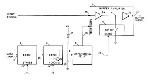
Figure 1 is a block diagram of a switch which is
constructed according to the preferred embodiment of
the present invention and which is suitable for fabri-
cation as a monolithic device. A latch 1 receives a
data signal at data input terminal 11, stores said data
upon receipt of a strobe signal at strobe ~clocX) input
terminal 13, and presents the stored data to latch 3
via line 15. Latch 1 may comprise any of a number of
well known D-type fiip flop circuits with a digital
"one" received at strobe input terminal 13 comprising
the strobe signal. A digital "one" at data input
terminal 11 comprises a command for the switch to turn
on and, thereby, to conduct a ~elected signal from
input port 27 to output port 37.
The data signal present on line 15 is received by
a latch 3, which may comprise another D-type flip
flop, and i~ applied to line 21 upon receipt o a clock
~ignal at a clock input terminal 19- The data ~ignal,
as modified by capacitor 23 and current source 17, on
line 21 i8 presented to a differential delay circuit 5.
A delayed data signal and it6 inverse are presented by
circuit 5 to lines 35 and 25, respectively. The oper-
ation of differential delay circuit 5, ~nd the timing
~.Z7~i~i9Z
--4--
relationships of latches 1 and 3, will be discussed
below ~ith reference to Figures 4 and 5.
An incoming signal is received at input port 27 of
a buffer amplifier 9 and, depending upon the state of a
swi~ch 7, is either conducted to output port 37 via
amplifiers 29 aQd 39 or it is interrupted as discussed
below. A delayed data signal on line 15 is received at
the state input terminal 36 of switch 7 and causes
switch 7 either to open or close depending upon the
strobe, clock, and data signals received by latches 1
and 3. If switch 7 is closed, node 41 between ampli-
fiers 29 and ~9 is ~rounded thus interrupting the
transmission o~ the signal between input and output
ports 27 and 37. When switch 7 is closed, the signal
on Line 25 received at the program input terminal 26,
causes the current sources internal to buffer ampli-
fier 9 to enter an idle state and thus require consider-
ably less power than is required during conductance of
a 6ignal between input and output ports 27 and 37. The
timing relationship of switch 7 and buffer amplifier 9
will be discussed below with reference to Figure 8.
The ccmbination o the output transistor 20 of
~tch 3, curren~ source L7 and capacitor 23 causes the
buffer amplifier 9 and 6witch 7 to ta~e longer to
interrupt the transmission of the 6ignal between input
~nd output port6 27 and 37, than it does to initiate
such a trAnsmi6sion. Since capacitor 23 is directly
~cross transistor 20, the volt~ge on line 21 fall6 very
quickly when transi6tor 20 i~ turned on to initiate the
conduction of the ~ignal through buffer ~mplifier 9.
However, when tr~nsi6tor 20 turns off, the rate of
ch~rge of capacitor 23 is limited by the ~mount of
current ~v~ilnble from current 60urce 17. Thu6, the
interrupt~on of the transmission of the 6ignal through
buffer ~mplifier 9 cannot be ~niti~ted until capacitor
23 chnrge~ to the preset thre6hold voltage of differ-
cntinl del~y 5. Thi~ then permit6 the ~dju6tment of
i.Z~692
the ratio of the turn-on and turn-off times of the
signal transmission. The reason for the difference in
turn-on and turn-off times will become clear in the
discussion with respect to Figures 2 and 3.
Fiq~re 2 is a b1ock diagram of a simple three by
three signal routing system, which uses nine switches
of the type depicted in Figure 1. Note that turning on
any given switch connects the output signal of a single
signal source to a single signal receiver. For simplic-
ity, each of the switches Sij are shown having only
input and output ports 27 and 37, respectively. The
data, strobe and clock lines have been omitted and are
shown in Figure 3 without the signal lines shown here.
Figure 3 shows the control line connections used
in the routing system depicted in Figure 2. It ~hould
be noted that the sys~em uses a common clock-line which
ensures that all of the switches change simultaneously.
If the routing system is used to interconnect video
sources and receiver6, the clocking is typically done
during a vertical flyback portion of a video ~ignal so
as not to disrupt the transmitted picture. Each row o
switches uses a common data line ~connected to data
input ter~inals 11 shown in Figure 1) ~nd e~ch column
uses a common 6trobe line (strobe input terminals 13 in
Figure 1). By suitably timing the ~pplication of data
~nd 6trobe pulses, t~e next 6tate of each individual
6witch c~n be preset ~synchronou61y with the final
~tate change acco~plished 6ynchronously by the clock
pul6e. ~hus, ~ three by three ~atrix u6es seven con-
trol lines (three dat~ l~nes, three ~trobe lines, andone clock line) nnd ~ ten by ten matrix uses only 21
control llne6 (Sen dat~ lines, ten ~trobe l~ne6 ~nd one
- clocX line).
Figure 4 i8 A schematlc di~gr~m of differenti~l
del~y clrcuit S ~nd ~ portion of l~tch 3 ~8 shown ~n
Flgure 1. The data pulse, clocked by the clock pulse,
i~ ~pplLed to the base of ~ tr~nsl~tor 20 in latch 3.
~ Z~ 9Z
Transistor 20 may comprise a high speed device having
Schottky junctions. The emitter ~f transistor 20, and
its collector through a capacitor 23, is connected to a
-Vc voltage supply. The collector is also connected to
a +Vc voltage supply through a current source 17 which
may easily be constructed by persons of ordinary sXill
in the art. The collector of transistor 20 via line 21
is further connected to the base of a transistor S7.
The collector of transistor 57 is in turn connected to
line 35 to control switch 7. Transistor 57 is con-
nected to transistor 59 as 8 differential pair with the
collector of a transistor 67 connected to each of their
emitters. The emitter of transistor 67 is connected
through a resistor 69 to the -Vc voltage supply.
The collector of transistor 59 is connected to the
+Vc voltage supply through two serially connected
diodes 61 and 63 and a resistor 65~ The base of trans-
istor 59 is connected to the -Vc voltage supply through
three serially connected diodes 71, 73, and 75. The
collector of transistor 59 is also connected to line 25
to program up or down the current sources of buffer
amplifier 9 as necessary. The base of transistor 67 is
connected to the base o a transistor 77. The col-
lector of transistor 77 i8 connected to line 2S and the
emitter of transistor 77 i5 connected, through a
resistor 79, to the -Yc voltage 6upply. The base of
transistor 77 i8 connected to current source 83, the
other end of which is connected to the -Vc voltage
supply. The base of tran~istor 77 i6 al~o connected to
the emitter of a tr~nsistor 81. The collector of
trnnsistor Bl is connected to ground and the base of
transi6tor 81 is connected to ground through ~ re~istor
89. The ba6e of transistor 81 i~ also connected to the
-Vc voltage supply through a resi~tor 91 and a diode
93.
~ he operation of differential del~y circuit 5
6hown in Figure 4 may be bettcr under~tood wi~h addi-
tional reference to Figure 1 nnd to ~he timing dingram~
i69;~
of Figures SA-H. The base voltage of transistor 20 of
latch 3, shown in Figure SE, goes from low to high when
a clock pulse (Figure SD) occurs at clock input terminal
19 and the data signal present on line 15 (Figure 5C)
from latch 1 is high due to a simultaneous occurrence of
a data signal (Figure 5A) and a strobe pulse (Figure
SB). ~he output signal of differential delay circuit 5
on line 25 (Figure SF) goes from high to low as the
output of latch 3 (Figure SE) goes from low to high.
But, the low to high transition of the output signal of
differential delay circuit S on line 25 is delayed from
the high to low transition of the output of latch 3.
This means that, in a routing system of the type shown
in Figure 2, every signal receiver is always connected
to at least one switch that is turned on if at least
one video switch in each column is turned on. Ihus,
the generation of 6purious voltage spikes in the output
signal due to clamping the output signal to a negative
D.C. voltage is avoided. Since lines 25 and 35 are
connected to the collectors of transistors 59 and 57,
respectively, and ~ince those ransistors are connected
in a differential pair, the sisnal on line 35 i6 the
inverse of the signal ~hown in ~igure SF.
When a low to high transition occur6 on the ba6e
of transistor 20, t~e base voltage of transiRtor 57 is
allowed to fall quickly through tran~istor 20. On the
other hand, when a high to low tr~n6ition occur~ on the
ba~e of transistor 20, the base voltage of transistor
57 ramp~ up rel~tively 610wly due to the charging of
capacitor 23 by current source 17. If the voltage on
the base o~ tr~n~istor 20 i~ high, indicating that the
3witch ha~ been turned ~n (conaucting the ~ignal ~pplied
to port 27 to port 37), tran~i~tor 20 turns on ~nd
transistor 57 turns of~. Thi~ c~uses e3~entially zero
current to flow on line 35 and through transi6tor 57.
If the voltage on the basc of tr~n~i~tor 20 iR
low, lndicating that the nwit~h i~ to interrupt the
~Z~7~
signal before it reaches output port ~7, transis~or 20
turns off, transistor 57 turns on, and current flows on
line 35 into the collector of transistor 57. 8ecause
of transistor 67, a constant total emitter current
flows through the differential pair composed of trans-
istor 57 and 59. The result is that, as the voltage on
line 21 goes from low to high, and transistor 57 goes
from off to on, the amount of collector current flowing
on line 25 through transistor 59 goes from a high value
to a low value.
Figure 6 is a schematic diagram of switch 7, shown
in Figure 1. The state input of switch 7 receives a
state control pulse, via line 35 from differential
delay circuit 5. This pulse is coupled to the base of
a transistor 107, and the base of transistor 107 is
coupled to the junction of diode 103 and current source
101 which, in turn, are coupled to ground and the +Vc
voltage supply, respectively. The emitter of trans-
istor 107 is tied to ground and the collector of trans-
istor 107 is tied, through current 60urce 105 to the
+Vc voltage supply.
The collector of transistor 107 is al o connected
to the base of a tran~istor 109, the emitter of which
is tied to ground. Node 41, also 6hown in Figure 1, is
taken ~rom the collector of transistor 109. Transi~tor
107 and 109 may ide~lly compri6e device6 fabricated
w~th Schott~y base-collector clamp diodes to avoid
6ubstrate current due to s~turation.
~he operation of the circuit nhown in Figure 6 may
be best understood with addition~l reference to Figure6
1, 4 and 5. Switch 7 closes (transi6tor 109 conducts),
effectively grounding node 41, when the data 6ignal on
qnput termlnal 11 is low (diqital ~ero~) tFigure SA)
~nd a ~ubsequent strobe ~Figure 5~) ~nd clock ~Figure
SD) pulses (digital ~unes~) ~re received ~t input
terminals 13 and 19, respectively. It ~hould be noted
that ~uch ~ ~equence of ~ignal~ cau~e6 the collector
lZ 7&6~Z
voltage of transistor 20 (Figures 4 and SF) to ramp up-
wards. When the colLector voltage of transi~tor 20
reaches a predetermined threshold voltage, set by the
biasing of transistor 59 and the resu~tant collector
current thereof (differential delay 5), transistor 57
turns on and sinks current from line 35. ~his, in
turn, turns transis~or 107 (Figure 6) off. With trans-
istor 107 off, the base voltage of transistor 109 is
allowed to increase and transistor 109 turns on. Since
transistor 109 is a low saturation voltage device, when
it is turned on, node 41, and the signal thereon, is
essentia~ly grounded as desired, interrupting the
transmission of that signal to output port 37. Simi-
larly, ~witch 7 opens when a digital "one" is received
~t.data input terminal 11 and the subsequent 6trobe and
clocX pulses are received at input terminals 13 and 19.
Figure 7 is a ~chematic diagram of buffer ampli-
fi`er 9 6hown in Figure 1. Input port 27 is connected
to the ba6e of a transistor 163, the emitter o~ which
20 i6 connected through current source lSl to the -Vc
voltage 6upply.
The.emitter of transistor 165 is connected to the
-Vc voltage 6upply throu~h current 60urce 15, and its
collector i6 connected to the +Vc volt~ge 6upply. ~he
emitter of transistor 165 is also connected to the ba6e
of a transl~tor 181. The collector o~ transistor 181
~8 connected through three 6erially connested diodes
183, 185, and 187, to the emitter of transi6tor 163.
The em~tter of transS6tor 181 i6 connected through the
co~lector-em~tter p~th of ~ transi6tor 173 nnd ~
re~to~ 171, to the +Vc voltage ~upply. The emitter
of.trnnnS~tor 181 iB ~160 connected to the ~Vc volt~ge
~upply vi~ the emitter-collector path of ~ tr~n6~6~0r
179. Tr~nsl6tor 179 han two collector~ of equal ~re~
w~th one of ~d collector6 belng connected to the +Vc
voltage ~upply. ~he ~econd collector of transi6tor 179
S 6 d~ode connected to the ba6e of transl~tor 179. The
i6~2
--10--
base of transistor 179 is connected to the collector of
a transistor 175, the emitter of which is connected to
the base of transistor 173.
The base of transistor 175 is connected to the
program input line 25 from the differential delay
circuit 5. Program input line 25 is also connected to
the base of a Darlington pair 203 and to the base of a
transistor 20S. The emitter of Darlington pair 203 is
connected to the +Vc voltage supply through a resistor
201. The collector of transistor 205 is connected to
the +Vc voltage supply and the emitter of transistor
205 is connected, through a diode 207, to the collector
of transistor 209. The collector of transistor 209 is
also connected to the base of transistor 165. The base
lS of transistor 209 is connected to the collector of
Darlington pair 203. The emitter of transistor 209 is
connected through a serial~y connected diode 217 and
resistor 219 to the -Yc voltage supply. The base of
transistor 209 is also connected to the -Vc voltage
6uppLy via the serially connected combination of diodes
211 and 213 and resistor 215~
The collector of transistor 221 is connected to
the +Vc voltage supply. The base of transistor 221 is
connected to the collector of transi~tor 181 and is
2S also connected to node 41. The emitter of transistor
221 i8 connected to the -Vc voltage supply through
current 60urce 223.
Output port 37 is connected to the emitter of a
tran~istor 229 with the collector of transistor 229
connected to the +Vc voltage supply. The base of
transistor 229 i~ connected to the emitter of trans-
i~tor 221 through ~ resistor 227.
- The operation of the circuit shown in Figure 7 may
be be~t understood with additional reference to Figures
1, 4, ~nd 6. When it i~ desired that buffer amplifier
9 conduct a signal from input port 27 to output port
~ Z)766~2
37, transistor 109 (Figure 6) i6 turned off (switch 7
ope~s) and the volta~e at node 41 is allowed to float
as required. Further, since transistor 57 ~Figure 4)
i~ also turned off, transistor S9 passes all of the
co~lector current of transistor 67. This current
together with the collector current of transistor 77
flows out of buffer amplifier 9 into differential delay
circuit S via line 25 (Figure 1). That current turns
on transistors 175 and 179 (~igure 7) and the current
mirror formed by Darlington pair 2G3. In turn, current
sources lSl, lS9 and 223 are turned on and buffer
amplifier 9 is prepared to transmit a signal between
input port 27 and output port 37. ~he signal is receiv-
ed at input port 27 and is passed via transistors 163,
lS 221 and 229, and diodes lB3, 185, and 187 to output
port 37.
When it is desired to turn off the ~witch, node 41
(Figure 6) is grounded by turning on transistor 109,
~nd the current 60urce6 lSl, lS9 and 223 within buffer
~mplifier 9 ~re reduced to an idle condition. Under
these conditions, the emitter of transistor 163 is at
-0.7 voLt6 which causes diodes 183, l~S and 187 to be
non-conductive, the emitter of transi~tor 221 goes to
-0.7 volt6, which ~n turn turns tr~n~i6tor 229 off.
~his result6 in the lnterruption of the transmi6sion o~
the 6ign~1 from the lnput port 27 to output port 37.
Further, 6lnce transi~tor 57 (Figure 4) is turned on in
thl6 c~6e, the current flowing into line 25 i8 deCrea6-
ed, Thi6 means that the current flowing out of d~ffer-
enti~l delny clrcuit 5 on program line 25 (Figure 7) i~
o decrea~ed. Note th~t the amounts o~ the idle ~nd
conducting current6 on progra~ line 25 can be se~ with
- re6i6tor6 79 ~nd 69 (F~gure 4). When the ~bove di6cu~-
: ~ed clrcuits were tested, ~n ~dle current of 800
micro~mpere6 was mezsured for ~ 7.5:1 decre~6e in
power con~umption of the switch ~n the ~dle st~te
rel~tive to the conductlng 6tate.
~ 2761~2
-12-
It is important to note ~hat the circuit shown in
Figure 7 allows ~ignal path (port 27 to port 37) trans-
ition times on the order of 100 nanoseconds with circuit
performance being largely independent of variations in
the betas of the PNP transistors utili~ed.
It is important to also note that, although the
switch current goes to an idle level when the signal
transmission is interrupted, the current sources and
transistors of buffer amplifier 9 are never turned off.
Thus, no time is lost on turn-on as a result of junc-
tion capacitances having to be charged in order to make
the transition from a grounded to a conducting state,
thus transition times on the order of 100 nanoseconds
can be achieved.
The performance of the above-discussed circuit is
depicted in the diagrams of Figure 8. As discussed
above, the relative currents of buffer amplifier 9 can
be preset with various resistors.
Since a large signal routing ~ystem or matrix may
include many thousands of crosspoint ~witches, at is
desirable to minimize both the the 6ize and power
requirements of such switches. Switches designed as
di~cussed above can be manufactured in a monolithic
structure to achieve both of those desired res~lts. In
2S fact, much of ~he circuit configuration discu~sed above
was derived to optimize the monolithic 6witch 60 that
it performs a8 desired. This i8 particularly true in
the bufer ~mplifier 9 ~ec~ion ~hown in Figure 7.
The m~in problem which must be overcome in any
monolithic atructure i8 the problem of not being ~ble
to generate lateral PNP devices with a high beta. To
o~ercome this problem, the currents p~rticularly in the
buffer amplifier 9 ~ection must be well defined to ma~e
the off~ets work out correctly which requires well
defined currents ~o ~hat the entire circuit will be
tolerant of the very low beta of the lateral PNP device3
in n monolithic ~tructure ~nd yet ~aint~in ~ fairly high
1 ~'7~
yield of the devices 80 produced, the attempt here was
to produce a circuit which could be turned on and off
~uickly without instability or oscillation and one that
didn't have erratic behavior during the turn-on and
S turn-off cycles. To achieve that result two current
mirrors were included in the circuit for buffer a~pli-
fier 9 as shown in Pigure 7. Referring again to Figures
4 and 7, note that current programming line 25 between
differential delay S and buffer amplifier 9 is con-
nected to the +Vc voltaye source through diodes 61 and
63 and resistor 65. The impedance of these devices
together with resistor 69 selects a voltage level for
the programming line 25. Current programming line 25
may also be referred to as the base bias line for
Darlington transistor ~03 and transistor 175. ~arling-
ton transistor 203 is connected as a current mirror
which reflects its base current to the current 60urces
lSl, 159 and 223 connected to the -Vc voltage supply.
Transistor~ 173 and 17S form a 6econd current mirror
which could have been fed directly to the diode string
183, 185, 187 except that this would cause the col-
lector of Darlington transistor 203 to 6wing at a high
frequency which would resuLt in the signal at the anode
of diode 183 being distorted because of the collector
to base capacitance of transistor 175 and it6 low cut-
off frequency.
To eliminate th~t problem, the current from the
second current mirror, ~ncluding transi6tors 173 and
175, Ls applied to ~ ca~code stage including translstor
181 wlth the ba~e of transistor 181 tied to the -Vc
volt~ge ~ource through current 60urce lS9. In this
configuration the b~se of tr~nsistor 181 iB connected
to ~ low impednnce point, thu-~ bloc~ing the possibility
of d~stortion. However, the low beta of the l~teral
PNP tr~nsistors causes the b~se current of transistor
181 to degenerate, ~nd thus, making its collector
current inaccur~te. To overcome thi~ problem it iB
~ ~766~Z
-14-
necesYary to introduce a current back ~nto the emitter
of transistor 181 to compensate for its own base cur-
rent loss. To achieve this, NPN transistor 179 is
designed to have two collectors of equal area. One of
S those collectors is diode connected to the base of
transistor 179 and the second is connected to the +Vc
voltage supply. The diode connected collector of
transistor 179 sets up a base emitter voltage which
will double the emitter current of that transistor
relative to its collector current. Since transistor
179 is looking at the collector c~rrent of transistor
175 which is translating the base current of 173, one
times the collector current of transistor 175 is ap-
proximately one times base current of transistor 173,
60 the emitter current of transistor 179 is 2 times the
base current of transistor 173. That then qets added
into the emitter current of transistor 181. This
con-figuration then provides us with an accurate current
representation through diodes 183, 185 and 187 of the
current on programming line 25 for variations in the
betas of the PNP devices in the monolithic 6tructure.
In this configuration the lateral PNP devices of the
monol~thic 6tructure are nll in a feed forward con-
figuration 80 that the tran Ltion from the standby
current mode to the conduction of buffer amplifier 9 is
very rapid. Experiment~lly th~ 6 has been observed to
take only 100 nano~econds.
Figure 7a shows a transistor circuit 179', ~n
alternate lmplement~tion of the two collector tran~-
l~tor 179 of Figure 7. Thi~ implementat~on includestwo tr~nsi~tors 179a and 179b which must be m~tched to
achieve the two ldentic~l collector current~ ~s dis-
cu~sed above. To achieve the nece~ary matching of
transistors 179a ~nd 179b they must have subst~nti~lly
the same ba~e-emitter junctions and ~ubut~ntially equal
collector are~. Transistor~ 179~ and 179b, in order
~Z76692
to simulate the operation o~ the two col7eetoc transistor
179, have their bases oonneeted one to the other, to ~orm
terminal C', their emitters eonneeted one to the other to
form terminal ~', the eolleetoc o~ transistoc l79b
S eonneeted to the intereonneeted bases, and the colleetor
of transistor 179a ~orming teeminal B' o~ transistoc
eircuit 179'. In replaeing transistor 179 in Figuce 7
with tcansistoc eireuit 179', terminals A', B' and C'
would be eonneeted to nodes A, 8 and C o~ ~igure 7,
l~ respeetivelY-