Note: Descriptions are shown in the official language in which they were submitted.
1- ~1256 CAN 5
Description
Microprocessor Controlled Signal Discrimination Circuitry
Technical Field
The invention presented herein relates to
circuitry for the validation of repetitive sig~als such as
those initiated by an optical energy emitter mounted on a
vehicle wherein the circuitry is useful in a traffic signal
control system,which can be remotely changed from a normal
10 traffic mode of operation to an optical energy emitter mode
of operation and, more particularly, to the use of a
microprocessor as a part of such circuitry.
Background Art
U.S. Patent Re. 28,100 discloses a traffic signal
15 remote control system in which a pulsed beam of high
intensity light transmitted at a predetermined frequency
from an emergency vehicle is detected at a controlled
traffic intersection and is used to initiate the operation
of circuitry operatively connected to the traf~ic light
20 signal controller for the intersection so a green light will
be provided for the emergency vehicle. Such pulses of light
are distinguished from the steady state ambient light by the
use of a detector which responds only to light pulses which
increase in intensity at a very fast rate. The possibility
25 of the system responding to false signals is reduced further
by integrating the signals received so a number of the
pulses must be received within a short time to provide a
signal of sufficient magnitude to cause the remote control
system to provide the desired control of the traffic light
30 signal controller.
It was found that the signal discrimination
provided by the system described in the above-mentioned
patent does not adequately discriminate between a series of
equally spaced light pulses and a series of irregularly
35 spaced light pulses. U.S. Patent 4,230,992 discloses a
signal discriminating circuit that provides the needed
~'
0
--2---
discrimination, but requires the use of a number of
discrete, dedicated circuits.
Disclosure of Invention
The invention presented herein provides
circuitry for distinguishing signals initiated by an
optical energy transmitter mounted on selected vehicles
from other signals initiated by other light sources such
as fluorescent lights, neon signs, mercury vapor lamp and
lightning flashes without using a large number of
discrete, dedicated circuit portions.
The invention presented herein provides for
circuitry for the validation of repetitive signals
supplied to the circuitry which includes a programmable
microprocessor connected to input/output circuitry, a
random access memory, and a read only memory (ROM) for
storing instructions for the programmable microprocessor.
The input/output circuitry has a plurality of inputs and
provides information as to when and which of the inputs
receives a signal. The programmable microprocessor is
programmed for operating with the input/output circuitry
and the random access memory for controlling the
input/output circuitry for permitting any of said signal
inputs to receive a signal and when a signal is received
at one of said signal inputs providing a "lock-outl' time
interval during which none of said signal inputs can
receive a signal and upon completion of said lock-out time
interval establishing a "window" time interval during
which a signal can be received only at said one of said
signal inputs, said "lock-out" and "window" time intervals
being provided each time a signal is received at said one
of said signal inputs permitting any of said signal inputs
to receive a signal in the event a signal is not received
during a "window" time interval, a signal received to
establish said one of said signal inputs being considered
valid by said programmable microprocessor when a
predetermined number of signals are received at said one
of said signal inputs before a "window" interval is
provided during which a signal is not received at said one
of said inputs.
~277~
--3--
Brief Description o~ the Drawings
A better understanding of this invention including
its novel features and utility will be obtained upon the
consideration of the following detailed description and
5 accompanying drawings wherein:
Figure 1 is a showing in block diagram form oE
circuitry embodying the invention;
Figures 2 and 3 set forth a flow chart for the
programming of the microprocessor of Figure 1 for operation
10 of the circuitry of Figure 1 in accordance with the
invention; and
Fig~re 4 shows how Figures 2 and 3 are arranged
for a full showing of the flow chart.
Detailed Description
The invention presented herein is embodied in the
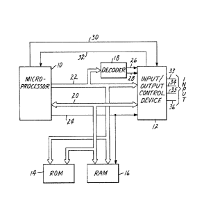
circuitry shown in block diagram form in Figure 1 wherein
the microprocessor 10 of the circuitry of Figure l is
programmed in accordance with the flow chart that is set
forth in Figures 2 and 3. A full showing of the flow chart
20 is obtained when Figures 2 and 3 are arranged as shown in
Figure 4. In addition to the microprocessor 10, the
circuitry of Fi~ure 1 includes input/output control
circuitry 12, a read only memory (ROM) 14 or microprocessor
instructions, a random access memory ~RAM) 16 and a decoder
25 18. The microprocessor 10 is connected via a data bus 20 to
each of the circuit portions mentioned, except the decoder
1~. In addition, an address bus 22 is provided between the
microprocessor 10 and each of the other circuit portions of
Figure 1. A connection 24 is also provided between the
30 microprocessor 10 and the input/output control circuitry 12
as well as the RAM 16 via which the microprocessor 10 can
establish the read or write mode of operation, as required,`
for the circuitry 12 and RAM 16.
Suitable input/output control circuitry 12 can be
35 provided by use of an R65C22 versatile interace adapter
that is available from the Rockwell Corporation, 4311
Jamboree Road, P.o. Box CMS 501-300, Newport Beach,
~;~77~)41:)
--4--
California 92658-8902. The circuitry 12 provided by the
R65C22 versatile interface adapter includes two chip select
inputs which are connected via connections 26 and 28 to
receive address signals from the microprocessor 10 via the
5 decoder 18 for addressing various registers th~t are
available in the R65C22. Clock signals from the
microprocessor 10 are supplied to the circuitry 12 via the
conductor 30. An interrupt signal is supplied from the
circuitry 12 to the microprocessor under certain conditions.
10 It is supplied via the conductor 32. The input/output
circuitry 12 is used for receiving pulse signals at any of
four signal inputs 33-36. The pulse signals of interest are
those produced in response to the receipt by circuitry (not
shown) of high intensity light transmitted at a
15 predetermined frequency from a light pulse transmitter
m~unted on a vehicle. It is possible, however, for other
pulse signals to be produced in response to various light
sources. Each pulse signal that is received by a signal
input 33-36, provided the input receiving the signal is
20 open, i.e. free to receive a signal, causes an interrupt
signal to be provided to the microprocessor 10.
The circuitry of Figure 1 functions in response to
programming of the microprocessor 10 in accordance with the
flow chart or dia~ram set forth in Figures 2 and 3 to
25 determine whether pulse signals received at any one of the
signal inputs 33-36 are the result of light transmitted from
certain light transmitters. This function is carried out by
monitoring all four si~nal inputs 33-36 for the receipt of a
signal pulse initiated by a light pulse and notifying the
30 microprocessor 10 via the interrupt line 32 when the first
pulse is received at one o~ the ~our signal inputs. The
microprocessor 10 then communicates with input/output
circuitry 12 to determine which of the signal inputs 33-36
received the pulse signal. The validation of signals
35 received at any of the signal inputs 33-36 is based on the
fact that a valid source for the light initiated pulses to
be detected will produce a series of equally spaced pulses
~77~46)
-5
at a known frequency. When a first pulse signal has been
received, the microprocessor 10 provides for the closure of
the signal inputs 33-36 for a "lock-out" time interval using
a timer register that is provided as a part of the
5 input/output circuitry 12. The "lock-out" time interval
established is equal to the minimum time interval expected
between successive pulses produced by a valid source. This
time interval for closure of the signal inputs 33-36 serves
to preclude recognition of the receipt of any pulse signal
10 during such "lock-out" time interval that may have been
ini~iated by an invalid optical signal source. Upon
termination of this "lock-out" time interval, another time
interval, which is much shorter, is provided. This interval
together with the "lock-out" time interval equals the
15 maximum ti~e that is expected between successive pulse
signals from a valid source. It is during this short time
interval or "window" time interval that a pulse signal
should be received from a valid source at the same input as
the first pulse signal is received. When the "window" time
20 interval is established, the input at which the first pulse
signal was received is opened for the "window" time
interval. A "lock-out" time interval followed by a "window"
time interval is established each time a pulse signal is
received during the preceding "window" time interval. If a
25 predetermined number of pulse signals are received during
successive "window" time intervals at the input at which the
first pulse signal was received, the pul~e signals are
considered valid. A ccunt is kept in a pulse signal count
register established in the RAM 16. Once the predetermined
30 number of pulse signals are received, this occurrence and
identification of the input receiving the pulse signals is
placed in an pulse signal ~ueue register established in the
RAM 16. In the event a pulse signal is not received as
expected during a "window" time interval, the pulse signal
35 count register is cleared and all signal inputs 33-36 are
opened to await the receipt of a "First" pulse signal at one
~277~)~0
--6--
of the signal inputs 33-36 with foregoing validation
functions carried out once again.
Figures 2 and 3 set forth a flow chart for the
programming of the microprocessor 10 in conjunction with the
5 other circuitry of Figure 1 to establish the signal
validation or discrimination functions that have been
discussed. Figure 4 shows how Figures 2 and 3 are arranged
to provide a full showing of the flow chart. The description
that follows ls provided with reference to the flow chart.
Assuming the first o a series of pulse signals is
received at one of the signal inputs 33-36 of the
input/output circuitry 12, an interrupt signal is supplied
via the interrupt connection 32 to the microprocessor 10, as
indicated at S0 in the flow chart. As indicated at 51, the
lS microprocessor 10 is required ~o determine whether it was an
interrupt from the input/output circuitry 12 due to the
receipt of a pulse signal at one of the signal inputs 33-36.
The input/output circuitry 12 includes two registers wherein
one register is an enable register which determines whether
20 stages in the other register, hereinafter referred to as the
pulse signal register, can be set and latched. The pulse
signal register has a stage for each of the signal inputs
33-36. If a stage is enabled, it is set and latched when the
input for the stage receives a pulse signal. The
25 microprocessor 10 establishes a primary input control
register in the RAM 16. This register has a stage for each
of the signal inputs 33-36 and is used to store information
regarding which of the stages for signal inputs 33-36 in the
pulse signal register of the circuitry 12 are enabled. It
30 also has a 1ag stage that indicates whether a pulse signal
for a signal input is the first pulse signal supplied to
such input. The microprocessor 10 also establishes a
secondary input control register in the RAM 16 which also
has a stage corresponding to each of the signal inputs
35 33-36. This secondary input control register is provided
since the program for the pulse signal validation or
discrimination routine is not the main program used by the
- ~.277~4~:)
--7--
microprocessor so a mechanism is needed to allow the main
program to prevail over the pulse signal discrimination
routine. The main program conditions the secondary input
control register to provide an indication to the pulse
5 signal discrimination routine as to which of the si~nal
inputs 33-36 can provide for a service request that will be
accepted. Referring again to the flow chart, since the
interrupt signal is determined to be a pulse signal
interrupt, step 52 is reached where the microprocessor
10 determines whether the pulse signal received was the first
pulse signal. Since it is the first pulse signal, a
determination is then made at step 53 as to whether the main
program will allow the pulse signal discrimination routine
to continue. The next step is 54 if the main program will
15 not permit the pulse signal discrimination routine to
continue. All inputs are opened at this step to again await
the receipt of a pulse signal at one of the inputs, t~e
first pulse flag stage in the pulse signal register in the
circuitry 12 is cleared and the routine is exited as
20 indicated at 56. Referring again to step 53, if the
microprocessor is allowed to continue the pulse signal
discrlmination routine, the microprocessor determines from
the input/output circuitry 12 which signal input received
the pulse signal, enters this information in the primary
25 input control register in the RAM 16 and clears the first
pulse flag in the pulse signal register in circuitry 12. The
routine then proceeds to step 58 at which point all of the
signal inputs 33-36 are closed. They will be closed for a
"lock-out" time interval since no pulse signals should ~ccur
30 for such time interval if the first pulse signal was from a
valid source. Due to the clock frequency of the
microprocessor 10, the selection of the RS65C22 adapter as
the input/output circuitry 12 plus the length o~ the
"lock-out" time required for discrimination of pulse
35 signals, a timer register or countsr in the RS65C22 mus~ be
set twice to provide the necessary "lock-out" time interval
when the pulse signals are to occur every 70 milliseconds.
7040
--8--
The flow chart reflects the two settings of the timer
register or counter to establish the "lock-out" time
interval, but could be changed readily to reflect a
situation wherein only a timer register or counter having
5 sufficient capacity is used to provide such time interval.
After closure of all of the signal inputs 33-36, as
indicated at 58, the timer register in the input/output
circuitry 12 is set for a "First" time interval, which is
less than the desired "lock-out" time interval and the timer
~0 reqister is started as indicated at 59. The discrimination
routine is then exited at 60 to free the microprocessor for
other routines. The completion of the "First" time interval
causes an interrupt signal to be supplied to the
microprocessor 10 from the timer register that provides the
15 "First" time interval. The query at 51 of the flow chart as
to whether the interrupt is an input interrupt must be
answered in the negative since all of the signal inputs
33-36 were closed prior to the start of the "First" time
interval. As indicated at step 61~ the query then is whether
20 the interrupt was from a timer register. If it were not, the
microprocessor 10 is free to proceed with whatever service
routine gave rise to the interrupt. In this case the
interrupt is from the timer register providing the "First"
time interval so the next step is 62 where a determination
25 is made as to what time interval has been completed. Since
the "First" time interval has been completed, the next step
at 63 requires the "Second" time interval to be set, i.e.,
the additional time interval needed to complete the
"lock-out" time interval. This "Second" time interval is
30 loaded in the timer register or counter provided in
circuitry 12 and is started as indicated at 64. The routine
is then exited as indicated at 65. Upon completion of the
"Second" time interval, which completes the "lock-out" time
interval, the timer register or counter causes an interrupt
35 signal to be supplied which is subjected to the queries at
51, 61 and 62. Since the answer to the query at 62 is the
"Second" time interval, the next step, which is 66, involves
~77~
g
setting the "Third" or "window" time interval. The next step
is ~7 at which time the "window" time interval is loaded
into the timer register and started. The microprocessor
establishes a pulse signal count register in the RAM 16 for
5 maintaining a current count of the number of consecutive
pulse signals received with provision made, as will be
discussed, to clear the count to zero if a pulse signal is
not received during a "window" time interval. Qnce the
required count is achieved, the count will be frozen so long
10 as consecutive pulse signals are received. Referring again
to the flow chart, a query is made at step 68 as to whether
the pulse signal count has been achieved. Since only the
first pulse signal has been received, the answer is no. This
being the case, the pulse signal count register is
15 incremented as indicated at step 69. The microprocessor 10
then communicates with the pulse signal enable register in
the circuitry 12 to provide for the initiation of an
interrupt in response to pulse signals received at only the
input at which the pulse signal just counted was received.
20 This is indicated at step 70. The routine is then exited at
71. This completes a discussion of the flow chart with
respect to the routine established in response to receipt of
a first pulse signal at one of the signal inputs 33-36.
Per the discussion above, the "Third" or "window"
25 time interval has been started. If a pulse signal is
received at the same signal input as the first signal, an
interrupt signal will be provided to the microprocessor in
view of the action taken at 70 in the flo~ chart. Receipt of
the interrupt signal occurs at step S0 of the flow chart and
30 since it is a pulse signal input interrupt the routine
proceeds to step 52 via 51. Since it is not the first pulse
signal, the routine is moved by step 52 directly to step 58
which calls for a closure of all of the signal inputs 33-36.
Proceeding to step 59, the "First" timing interval for a
35 portion of the "lock-out" time interval is loaded and timer
register started. The routine is then e~isted at 60 and the
routine continues from this point in the same manner as has
- - ~L277~
--10--
been described in connection with the consideration of the
routine with respect to the first pulse signal received.
Assuming additional pulse signals are received that are
valid pulse signals, a point will be reached where the
5 desired pulse signal count is attained, for example, 22.
This will be established at step 68. With the desired pulse
signal count achieved, the routine proceeds to the step 72
wherein a register having a stage for each of the signal
inputs 33-36 that is established in the RAM 16 is addressed
10 to have the register indicate that valid pulse signals have
been received at the input at which the pulse signals were
received. This register hereinafter shall be referred to as
the pulse signal queue register. The main program of the
microprocessor 10 will periodically read this register to
15 determine whether there is a stage in the register that
indicates a "call" has been registered so the main program
can respond to the "call" or clear the pulse signal queue
register forcing the pulse signal discrimination routine to
repeat the "call." A~ter the particular input at which the
"call" has been received is identified in the pulse signal
queue register, the routine proceeds to.step 7Q where action
is taken to permit interrupt signals based on pulse signals
received at the signal inputs 33-36 to be provided only from
the input that received the pulse signals giving rise to the
"call" placed in the pulse signal queue register.
One aspect of the routine set forth in the flow
chart that has not been considered is that p~rtion dealing
with the failure of the designated input to circuitry 12 to
receive a pulse signal before expiration of a "Third" or
"window" time interval that is established at various times
during the routine that has been discussed. Such failure
means the pulse signals input that have been received and
are being counted are considered invalid and must be
disregarded. If the "Third" or "window" time interval
expires without a pulse signal received at the designated
input during such time interval, the timer register will
provide an interrupt signal to the microprocessor to begin
~277~
the routine at 50 and as for expirations of the "First" and
"Second" time intervals the routine proceeds via steps 51
and 61 to step 62. At step 62 information regarding the time
interval that has expired is sought. In this case, it is the
5 "Third" timer interval that has expired so the routine
proceeds to step 73 wherein the routine directs the
input/output circuitry 12 to allow all pulse signal inputs
to receive pulse signals. At step 74 the routine provides
for the pulse signal queue register in RAM 16 to be cleared
10 before the routine is exited at step 75.
While there has been described what is at present
considered to be the preferred embodiment of the invention,
it will be understood that various modifications may be made
therein and it is intended to cover in the appended claims
15 all such modifications as fall within the true spirit and
scope of the invention.