Note: Descriptions are shown in the official language in which they were submitted.
~2t77~
1 64157-218
~ERMANO5ILI~ATE SPI~-ON ~LASS~S
Back~round of the Inv~ention
This invention relates to the field of semiconductor
processes that are compatihle with scaling down o~ devices to
smaller sizes and increasiny the complexity of the metal and
polysilicon interconnect patterns coupling various devices on the
dle to each other. More particularly, the invention relates to a
process for creatiny a planarized layer of germanosilicate ylass
between polyslllcon and some types of metal interconnect layers.
This invention will be described with re~erence to the
accompanying drawings in which:
figure 1 is a cross section of a polysilicon step on a
substrate covered with a CVD oxide layer and a spun-on coating to
illustrate the differences in flatness achieved by these two
techni~ues;
flgure 2 is a characteristic curve defining the
relationship between spin speed and film thickness;
figure 3 is cross-sectional view of the structure of a
typical structure ~ormed using the lnvention aonsisting of a first
layer interconnect of polyslllcon material .tnsulated from a second
layer of interconnect material made of metal by an intervening two
layers o~ spun-on binary yermanosilicate glass;
fiyure 4 is a process flow diagram for the process of
the invention;
figure 5 is an experimentally determined plot of the
deviatlons of layer thickness for the spun-on layers of binary
~2~
1 a 64157-218
glass deposited using the invention versus spin speed of the
application of the startlng solution.
One of the major problems in semiconductor device
fabrication is to make devices ever more complex without
increasing the size of the die. Increased dle slze decreases
yield and increases cost. However, to increase complexlty on an
integrated circuit die reyuires that thousands of transistors be
interconnected lnto very comple~ circuit patterns. The
interconnection patterns that result are very complicated and
involve many crossing conductors. However in integrated clrcuit
fabrication, conductors are usually formed in polysilicon or
metals like aluminum, titanium ox tungsten by photolithography
pxocesses. This involves projecting light patterns on a two
dimensional plane to form a two di.mensional pattern in the
conductor after performing certain etching steps that are well
known. This is fine as long as one desires that at every place
that two conductors cross each other that there be a circuit
connection. However, where two conductors which cross each other
are not supposed to be in electrical contact with each other,
there is a problem ln makiny a crossover or crossunder such that
the two conductors do not make electrical contact with each other.
These
.,, ~ c ~
--2--
problems grow in number a~ device complexity increases.
One way of alleviating this problQm is to add a second
layer of conductor over the firs~ conductor layer and
separating the two by an insulating layer. This process
of adding conductive layers can be repeated as many
times as necessary.
However these intermediate layers of insulating
material must be ~lat and of high integrity to be
effective. The insulating layer must ~e of high
integrity, i.e., no pinholes or cracks, 80 as to prevent
shorts between layers or open circuit~ in the layers
above it caused by ~ailure o~ the layers deposited above
to fill in the cracks in the insulator. The insulator
must be flat to have good photolithography
characteristics. Major problems are created in ~orming
~ubsequent layers using photolithography when trying to
project very ~ine and closely spaced patterns of light
onto a non-flat ~urface. Such problems include depth of
field difficulties and other well known problems.
Further, the insulating layer which is used
should be relatively free of dopants such as pho6phorus
which could come out of the insulating layer and enter
portions of the structure surrounding the insulating
layer during later high temperature processing steps.
Further, these intermediate insulating layers
must have a coefficient o~ thermal expansion which
substantially matches that of the underlying layer6.
This erevents cracking o~ the insulating layer caused by
uneven thermal expansions in di~erent layers in the
~tructure during later hi~h temperature proces6ing steps
or thecmal cycling during service of the device in the
~ield.
Many integcated devices today use doped
polysilicon ~or a ~irst conductive layer. In the prior
~27~
--3--
art phosphorous doped silicon dioxide or plain silicon
dioxide or germano~ilicate glasses have been deposited
over this polysilicon by chemical ~apor deposition or
low pre~sure chemical vapor deposition. This iB an
expen~ive and time con~uming process, not u~ually done
in a more e~ficient cassette to cassette opera~ion.
FurtheL, many of the gase~ used in the chemical vapor
deposition processes can be toxic, flammable or
corrosive or all three.
Further, many chemical vapor deposition
processes exhibit enhanced deposition at ~harp corners
under most reaction conditions. For example, Figure 1
shows an etched polysilicon ~tep 10 on a substrate 12.
~ film 14 of silicon dioxide has been deposited by
chemical vapor deposition. The line 15 6hown in phantom
repre~ents the ~ur~ace of a l~yer of spun-on glass, and
illustrate~ the differences in planarization which
result from the two different processes of depositing
insulating material. For che~ical vapor deposition
20 proces8es, the sharp points 16 and 18 of the polysilicon
step 10 cause increased chemical activity in these
regions, which results in the bulges 20 and 2Z being
foLmed in the film 14 near the corners 16 and 1~.
Immediately below these bulges, microcracks 24 and 26
can form- The8e crack8 are extremely difficult to cover
completely with metal, and can lead to open circuit~.
This bulge formation process is int~insic to the
chemical vapor deposition process undeL most
conditions. Further, this creates a non-flat surface
upon which to do subsequent photolithography. Non~flat
surfaces make the projection of light to deine images
in photoresi~t of clo~ely spaced conductors or other
features on subsequent layers dif~icult or impossible.
Further, non-flat suraces such as that presented by the
- 4 - 64157-21~
top sur~ace of the oxlde layer 14 with microcracks make it ex-
tremely difficult to deposit uniform films of metal with high
integrity, i.e., no cracks or crevices in the metal film which can
lead -to open circuits in conductors which are supposed to be con-
tinuous.
In contrast, notice the relatively smooth geometry o~
the top sur~ace 14 of the spun-on glass. This gent]y rolling
surface makes it simple to deposit high integrity metal Eilms ~rom
which interconnection wires can be formed with no Eear o~ open
circuits. Likewise, if another layer of spun-on glass is added,
the resulting sur~ace is flat or almost Elat, and photolithography
to form very fine features which are closely spaced becomes
possible.
Chemical vapor deposition processes are also high
temperature processes generally with typical reaction temperatures
~or formation of silicon dioxide films ranging from 400 to 900
degrees centigrade depending upon the gases and chemical reactions
used to form the film. These higher temperatures preclude use o
these processes over some structures which are temperature sensi-
tive. Further, these high deposition temperatures can causelateral and other undesired dif~usion o~ dopants previously in
other locations on the integrated circuit. This can cause un-
desirable e~ects such as changes in base width or channel length
ln transistors previously Eormed.
Finally, uniformlty oE Eilm coverage and ~latness in
regions removed Erom corners oE steps and trenches is generally
not consistent in chemical vapor deposition processes.
It is known that the CVD process can be avoided by using
a spin method to spin on coatings of silicon
64157-218
dioxide. In ~hese methods, a modified alcoholic solution of
tetraethoxygermane (hereafter TEOG) can be spun onto a silicon
wafer, heated appropriately and a glassy silicon dioxide film will
be formed. This eliminates some of the disadvantages of CVD and
LPCVD processe~, but leaves a major disadvantage. The major
problem wlth this technique is that above a thickness ranye of
approximately 3000 angstroms, the film develops cracks. These
cracks are totally unacceptable since they decrease yield and
render the devices unreliable.
Stress in films deposited on wafers is a function of the
degree of mismatch in the coefficient of thermal expansion and the
thickness of the film. Higher degrees of mismatch cause more
stress as do thicker films. Various modifiers can be added to the
solution, but useful thicknesses of 7,000-10,000 ê have not been
achieved to da~e.
Therefore a need has arisen for a method of depositing a
dopant free insula~or film that was ~lat, had high integrity, was
cheap and fast, and which could be deposited at a lower
temperature and which resulted in a film which had a good match in
thermal coefficient with the unflerlying structure.
According to one aspect of the present inventlon there
is provlded a process for forming a binary germanosillcate glass
on a wafer containing inteyrated circuits comprlsiny the steps of-
a. mixiny a predetermined solutlon oftetraethoxysilane, tetraethoxygermane, a solvent and an acid;
b. depositlny a predetermined amount of the solution on
said wafer;
.
.
~27~
5 a 64157-218
c. spinning ~he wafer un~il excess solutlon is spun off
the wafer and the remaining solution is in equilibrium;
d. bakiny the wafer and remaining solution until the
solvent is driven off and a binary germanosilicate glass is
formed.
According to a further aspect of the present invention
there is provided a method of forming an lnsulating film of
germanosilicate glass on the first lnterconnection layer of an
integrated circuit comprising the steps of,
a. mixing a solution of between 2~53 and 2.76 grams
tetraethoxygermane and between 2.47 and 2.24 grams
tetraethoxysilane with approximately 45 grams of an alcohol or
ketone and sufficient acid to raise the solution pH to between 1.5
and 2.0;
b. depositing a quantity of said solution onto a wafer
of silicon sufficient to create a puddle which covers the whole
surface of ~he wafer;
c. spinning the wafer for at least 30 seconds;
d. baking the wafer and remaining solution at at least
400 degrees centigrade for a sufficient time to drive off all the
solvents and to form a binary germanosillcate glass comprised of
45 to 50 percent germanium dioxide and the balance silicon
dioxide.
Accorcllny to another aspect of ~he presen~ invention
there is provlded a semlconductor structure which ls to he
lnsulated comprislng,
.: ~
.
~ . , ' .
5 b 64157-218
a first layer of conductive polysilicon material etched
into interconnect patterns having edges, said patterns forming
part of an integrated circuit;
a layer over said flrst layer of a soluti.on comprising
tetraethoxysilane, tetraethoxygermane, a solvent and an acid.
Summar~_of the lnvention
This invention is a process for deposlting an insulating
film over a polysillcon or some types of metal conductive layers
by a low temperature spin-on technique using a solution of TEOS
and TEOG in a solvent system which is pH controlled by the
addition of an acid. A 10% solution of TEOS and TEOG can be
dissolved in any of the lower alcohols and ketones as well as some
combinations of the two. Solution pH is adjusted by the addition
of an acid to bring the pH to approximately 1.5
--6--
to z.O to favor formation of a germano~ilicate gel
polymer. The gel is formed in the fiolvent ~oluticn at
the correct p~ and becomes apparent during the spinning
of the solution upon the wafer as a gel coating that can
then be hea~ treated to form the desired oxide or mixed
oxide ilm.
The ~olution i8 then spun onto a wafer upon
which the desired structures have already been formed.
After a minimum of 30 seconds of spinning, the solution
is evenly spLead out over the waer which tends to
smooth and flatten the waer topography. The iLst coat
tends to smooth out Eharp edges, while subsequent coat6
tend to create flatter surfa~es. The degree of flatnes~
can be con~rolled by using more coats.
Thereafter, a one or two ~tage baking step i~
performed to drive out the solvents and to form the
oxide~ from the gel.
In the preferred embodiment, a first ~tage
bake iB performed at approximately 135 degrees
centigrade for 5-10 minutes to drive out mo~t of the
solvents. Thereafter, a second stage bake at a
temperature in the range from 400 to 1000 degreefi
centigrade i8 performed to form and den~ify ~he oxide
film.
The resultant film is a very Plat, phosphorus
~ree binary glass comprised o ~5-50 mole peccent
germanium dioxide with the balance being silicon
dioxide. The film is Oe a uniPorm thickness with very
few pinholes, and it has a thermal expansion coeficient
which very closely matches that of polysilicon. The
presence o TEOG in the solution create6 the binary
germanosilicate gla~s. The presence of germanium
dioxide in the silica matrix raises the thermal
expansion coef~icient to a usePul match to that of ~he
~2~
7 64157-218
underlying polysilicon or epitaxial silicon when the glass
composition is nominally 50-50 mole percent germanium dioxide-
silicon dioxlde. The result i6 that very thick films on the order
of two microns can be fabricated over polysilicon and epitaxial
silicon wlthout formation of cracks. These thick films are very
important to forminq planarized insulation layers upon which to
project images for fuxther fabrica~ion. This planarization ls
very critical to scaling present sized technologies down to the
sub-one micron range for VLSI device ~abrication.
~L2~ 7
--8--
Detailed Description of the Pcefeceed Embodiment
In the pceferred embodimen~, a solu~ion of
TEOS, TEOG, a solvent such as a lower alcohol or a
ketone, and a compatible mineral or organic acid such as
nitric acid or hydrochloric acid is prepared. The
solution composition i8 aB follows:
*Z.53~2.76 grams of tetraethoxygeLmane (TEOG);
*2.47-2.Z~ grams of tetraethoxysilane (TEOS)
si(OC2~5)~;
*45 grams of solvent such as a lower alcohol or
ketone;
*0.03 grams compatible mineral or organic acid
such as HN03.
If 2.53 grams of TEOG and 2.47 grams of TEOS are used,
the resul~ant binary glass is 45 mole parcent germanium
dioxide and S5 mole peccent silicon dioxide. If Z.76
gcams of TEOG and 2.24 grams of TEOS are used, the
resultant binary glass will be 50-50 mole percent
gecmanium dioxide-silicon dioxide. Other solutions of
cour~e yield differing binary glass compositions. The
preferced composition i8 2.76 grams TEOG and 2.23 grams
TEOS with all other components being the same.
The solvent used is not critical to the
invention, and any solvent that will dissolve TEOS and
TEOG and be compatible with the spinning and firing
process will be adequate. Exameles of types of aicohols
that will work ace: ethyl, methyl, butyl, or propyl.
Examples of ketones that will work ace MEK and acetone.
That factors which matter ace the target mole pe~centage
composition of the cesultant binacy glas6 and the film
thickne~s thereof. The mole percent of the composition
of the binary glass that results depends upon the
relative amounts of TEOS and TEOG that were present in
the ociginal solution. Since any of these compounds
:~L27'7~7
g
that do not go into ~olution will not be in the final
composition, the ~olvent selected should be such the
solubility of TEOS and TEOG in it is such that the
selected amount of each compound dissolves completely.
If the solubility i6 othecwise, then the resultant
binary glass will not have the mole percent composition
intended for it.
Further, the film thickness depends upon the
viscosity of the solution and the spin,speed. The spin
~peed versus film thickness for a given viscosity of the
above ~olution is given by Figure 2. Note that the curve
assumes a 10~ TEOS and TEOG solution. Thus, the solvent
must be such that the resultant solution is 10~, which
is only true if the selected amounts of TEOS and TEOG
from the above ranges are totally di~solved in the
solvent ~uch that 10~ by weight of the 601ution is TEOS
and TEOG.
Genecally any of the lower alcohols and lower
ketones and some combinations of the two will meet the
above requirements. It i~ possible that other polar
solvent6 will al60 meet these requirements such as to be
functional equivalents. The preferred solvent is
absolute ethyl alcohol, but othe solvents are cheaper.
The particular acid used is not critical to ~he
invention as long as it is compatible with the other
component~ of the solution. Generally any mineral acid
with the axception of hydrofluoric acid can be used.
Obviou~ly adding an acid such as phosphoric or boric
acid would add these dopants, P or B, to the glass,
which may or may not be desirable depending upon the
application. A sufficient amount of acid must be added
to bring the pH of the solution to between 1.5 and 2Ø
This solution is spun onto a wafer conductor
structure or other structure which is to be insulated
~2~7~7
~10--
from the elements or from o~he~ layers which are to be
formed above it. The thickness of the layer to be
formed in this spin-on process i~ a matter of choice for
the designer depending upon the application involved.
The layer thickness can be controlled for any given
solution solid6 content and viscosity by controlling the
~pin speed at which the layer is deposited. Figure 2
illustrates the relationship between the spin speed and
the resultant layer thickness for a 10~ solution.
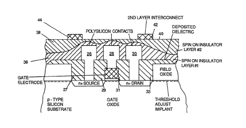
Figure 3 illustrates a typical circuit
structure over which the insulating film might be
applied. Figure 3 illustrates an MOS transistor with
polysilicon source, drain an~ gate contacts 26, za and
30 respectively. The typical situation wherein the
invention would be used would be to add another layer of
interconnects above the poly~ilicon contact layer of
which contacts 26, Z8 and 30 are a part. To do this, a
layer of insulator material must be formed over the
first layer interconnect polysilicon. This i~
accomplished using the invention as follows.
The second layer of interconnect structure will
have to be formed photolithographically by the etching
of the interconnect pattecn in a layer of metal or
polysilicon deposited on an insulating layer formed over
the first layer of polysilicon interconnects. To do
this photolithographic process properly, a flat or
gently rolling sur~ace on top of the insulating layer
over the first layer polysilicon must be formed. To do
this either a very thick layer of insulator must be
eormed or 8everal la~ers of in~ulator must be formed to
smooth out the sharp step junctions such as at the upper
co~ners of the polysilicon contacts 26, 28 and 30. As
noted with respect to the discussion of Figure 1, if CVD
oxide is depo~ited, the bulges 22 and 20 will ~e~ult
- 1 1
under many reaction condition~ at the corne~s of each of
the polysilicon contacts 26, 28 and 30. WorsQ yet, deep
crevices ~uch as the crevices 24 and 26 in Figure 1 ~an
form at the intersections of the polysilicon contacts
26, 28 and 30 with the CVD in6ulating oxide layers 27,
29, 31 and 33. These crevices woul2 be very hard to
fill when an overlying metal layer was deposited on top
o~ a CVD oxide layer. Indeed, these crevices would
likely result in a discontinuity in th~ metal covsrage
of the 8econd layer of metal. Thus CVD oxide is not a
very good choice for an intervening insulating layer
between two layers of interconnects.
The invention solves this crevice and bump
problem by eliminating the need for a CVD deposition.
This i6 done by use of a spin-on process to deposit a
solution which is turned first into a gel poly~e~ and
later into a binary glass. The final s~ructure of a
transistor using poly6ilicon contacts 26. 28 and 30 in a
ficst layer of interconnect structure and a second
interconnect layer of metal conductors ~2 and 44 is
shown in Figure 3. In Figure 3, the two layers of
interconnect structure are sepacated by a planarized
layer of spun-on binary glass comprised of two
separately spun-on layers 36 and 38 of binary
germanosilicate glasB. The step& of this spin-on
process will be described with reference to Figure6 ~.
Reeerring to Figure 4(A) the first step i~ to
prepare the solution defined above. Then the wafer
having the transistor 6tructure of Figure 3, or whatever
other structure that i6 to be covered, is placed in a
seinning device such as is conventionally used to s~in
on photore~ist. Known processes are used to form the
transistor structure of Figure 3 a6 it exl6ts prior to
the ~teps of 6pinning on the bin~ry germanosilicate
~77~
- 12 - 54157-218
glass forming solution described above. Spinning devices are well
known in the indus-try as -they have been used for years to deposit
photoresist films. The spinning process for photoresist is also
well known, and is described in detail by David Elliot in
Inte rated Circuit Fabrication Technolog~ (1982)(McGraw Hill Book
g
Company), Library oE Conyress Number I'K7874.E49, ISBN
0-07-01g238-3, at Chapter 6.
A quantity of this solution is then placed on the wafer
center and allowed to flow out to the edges o-f the wafer as
indicated by Figure 4(B). The wafer is then spun a-t the speed
necessary -to obtain -the desired film thickness as indicated in
Figure 4(C). As indicated at page 128 of Elliot, the film thick-
ness is a proportional -to -the square of the solids content of the
solution and inversely proportional to the square root of the spin
RPM. However, that formula is for photoresist, and the binary
glass forming solution used in the invention is slightly
different, although the relationship is still generally true. The
actual relationship between the spin speed and the resulting film
thickness is given by -the curve of Figure 2. In the preferred
embodiment, the desired film thickness is between 1400 and 1000
angstroms, which, by reEerence to Figure 2, -translates into a spin
speed of between 2000 and ~000 RPM. Since very precise control of
the spin speed can be maintained, the film thickness can be
controlled equally precisely. Note that the curve oE Figure 2
assumes a 10% TEOS & TEOG solution.
- 13 - 64157-218
There are several options available here for film -thick-
ness. If the underlyiny interconnect layer is polysilicon, then
the expansion coefEicient of thermal expansion of the binary glass
which will result will be very closely matched to that oE the
polysilicon. This allows a very thick film or several thin films
of the binary glass to be spun on since the stress in the film
wil]. be low, and there is little or no chance of cracking.
Stress in the film is related to the film thickness, the
relative match of the thermal expansion coefficients and the
deposition temperature among other things. A more detailed dis-
cussion of film stress will be found in S.M. Sze, ed., VLSI
Technology (1983) (McGraw Hill Book Company), Library of Congress
Nurnber TK7874.V566, IS~N 0-07-062686-3.
However, if the underlying first layer interconnect
material is metal, the thermal expansion coefficient match is not
going to be very good with the binary glass for some metals such
as aluminum. In such a case, a very thin film must be applied to
avoid cracking. Some metals such as tungsten have thermal
expansion coefficients which are a closer match with a germano-
2~ silicate binary glass however, and on these metals a thicker filmcan be deposited with less chance of cracking. The invention
finds its primary utility is spin-on deposition of binary glasses
over polysilicon conductive layers. In this situa-tion, the fi.lm
thic]cness can be very large compared to those Eilms which were
available in the prior art and no cracking occurs.
3L277~
- 13a - 64157-218
Alternatively however, several layers of spun-on binary
glass can be used over -the underlying polysilicon. This is the
situation depicted in Figure 3 where a first spun-on layer 36 of
binary glass is used to soften the sharp edges of the underlying
polysilicon steps. A second spun-on layer 38 of binary glass is
,.,~
~7~7
-14-
then used over the f irt layer to planarize the
insulating layer comprised of layers 36 and 3B to form a
.
flat surface 40. This flat surface makes an ideal
"sereen" upon which to pecform photolithogcaphic
opecations to form the second layer interconnect
structu~e. Metal conductors 42 and ~4 form part of this
second intecconnect layec, but these eonduetocs could
also be polysilicon if a third or fourth layer of
interconnect was to be u6ed.
The Bpin-on process gives great flatness of the
deposited films as illu~trated by Figure 1 surface 15
cornpared with the upper surface of the CVD oxide layer.
This flatness derive6 from the centrifugal force tending
to pull off excess solution and evenly distribute the
]5 solution aver the wafer 6u~face. Any ~ipples which try
to focm in the su~face have forces of ~urface ten~ion,
centcifugal force and adhesion to ~he surface which tend
to smooth them out, thereby creating a smooth surface.
The final step in the process of forming the
2b binary glass in~ulation layer between the two
interconnect layers is to bake the solution to dcive off
the solvents and to form the oxides in the binary
glass. In the preferred embodiment, the bake step
illustcated in Figuce 4(D) is pecformed in two stage~.
25 The fir~t stage is a low temperature bake at
appcoximately 135 degrees centigcade for 5-10 minutes to
drive off the solvents. The purpo6e of this bake is to
form the gel-like polymer which remains after the
solvents are gone from the solution. The chemical
reactions ~hat take place are uncleae, but it is known
that some formation of polymers takes place. The second
stage bake is preferably done at between 450 and 500
degrees cen~igrade for 15-30 minutes. The purpose of
this bake is convect the polymer gel into germanium
- 15 - 64157-218
dioxide and silicon dioxide. Higher or lower -temperatures can be
used, but this will change the time for the reactions to -take
place. Higher temperature~ yield a denser binary glass, i.e., the
compaction of the glass improves which gives it greater structural
integrity and higher resistance to the diffusion of unwanted
inpuri-ties into the struc-tures below. Greater density also
changes the etch rate of the binary glass. Fundamentally, any
temperature which will not damage the s-tructure below the binary
glass layer can be used. Higher -temperatures are generally better
unless there are implanted regions or other impurity doped regions
which might change dimension in an unwanted way during a high
temperature densification step for the binary glass.
Higher temperatures are not needed for flattening the
binary glass structure by reflow, however, since all flatness in
the structure is derived through the spin-on process alone. This
is the reason no phosphorous dopant is used in the binary glass.
Phosphorous dopant was used in the CVD deposited P-glasses of the
prior art to lower their melting temperatures sufficiently such
that they could be melted for reflow to smooth the surface for
easier photolithography and better metalization properties. But
the presence of phosphorous dopants crea-tes other processing
problems which are well known. Its elimination in the invention
is a significant advantage.
The next .step is to etch vias in the planariæed binar~
glass ~ormed by the bake step. This step is symbolized by Figure
4(E). This etch step can be by any conventional etch process
~277~
- 16 - 64157-218
which will effectively etch a binary glass comprised of 45-50%
germanium dioxide and the balance sillcon dioxide. Such process
are known. The advantage of the planarization of the surface 40
in Figure 3 is tha-t photolithography can be precisely performed on
it without suffering from depth of field problems which are nor-
mally encountered when projec-ting onto a non-flat surface. Such
problems are well known and result from the image being focussed
for a given distance rom the mask. If all portions of the sur-
face upon which the image is projected are not at the same dis-
tance from the lens, then portions of the image falling upon por-
tions of the surface which are closer to or farther from the lens
will be slightly out of focus. This problem spoils the sharpness
of the images which can be projected and limits the precision of
the con-trol of the geometry size that can be achieved and the
precision of the control of spacing between fea-tures which can be
reliably ac'nieved. Forming a flat surface such as surface 40 in
Figure 3 upon which to deposit photoresist causes the photoresist
to have a flat surface upon which a very sharp image of the de-
sired vias can be focussed. The spacing of these via images can
be as closer than in non-flat cases because the design rules can
be made tigh-ter in flat cases. The design rules can be tightened
without -fear of depth of field problems; these prob:lems arise from
Fuzzy def'inition of feature sizes, which may cause overlap oE
features that are not supposed to overlap.
The next step, as symboli~ed in Figure 4(F) is to de-
posit a layer oE material ~rom which to Eorln t'he second layer o~
.
- 17 - 6415~-218
interconnects. In many embod.iments where only two interconnect
layers are to be -formed, the second layer interconnect pattern
will be formed out of a metal such as aluminum. In embodiments
where more than two layers of in-terconnect are to be formed, the
second layer of interconnect materiaL is preferably polysilicon
since its coefficient of thermal expansion is a better match with
-the binary glass w'hich would be placed over it to insulate the
second layer po:Lysilicon from -t'he third layer of interconnect
materiaL.
The basic process to form the second layer interconnec-t
is -to first deposit a layer of the interconnect material such as
metal or doped polysilicon. Processes for depositing these layers
are well known and are described in chapter 9 of Sze's VLSI
Technology and in the ~lliott book. Any process to deposit -this
layer of conductive material which will give good conductor
integrity and reliability will suffice for purposes of practicing
the invention. That is, any method of metal deposition such as
physical vapor deposition, resistance heated evaporation, electron
beam evaporation, rf induction heated evaporation, sputter deposi-
tion, magnetron sput-ter deposition, or chemical vapor deposition
can be used if the method meets adequate quality standards for the
deposited metal :layer.
After t'he metal layer is deposited, a :Layer oE photo-
resist is deposited over the metal layer and exposed to radiation
t'hrough a mask containing the image of the desired metal inter-
connect pattern. Certain areas of the photoresist then cross-link
7~L~7
- 17a - 64157-218
and harden. The uncross-linked resist is then washed away in a
solvent leaving a hardened resist pattern on the surface of the
metal to act as an etch shield. The desired metal interconnect
pattern is then etched ou-t of the metal layer using a suitable
known etch process. This leaves the structure as shown in Figure
3.
The spin-on process yields an insulator film with good
ilm properties. One of these properties is uniformity of thick-
ness of the film over the thickness
~2~ 7
of the wafer. That is, re~erring to ~igure 3, the
variation of the thickness of the layers 3fi and 38 over
.
the wafer surface is le~s than 5% from any point on the
wafer su~face to any other point on the wafer surface
regardless of what speed the wafer was ~pun during the
film formation. Of course, if some structure on the
wafer surface has greatly projecting geometry, the
spun-on glass may not cover its uppermost point, and the
f ilm thickness will be zero or very small on the point
of such an unusual object. This may cause the 5%
maximum deviation figure cited above to be inaccurate
for this unusual case.
Figure 5 illustrate& the experimentally
determined fil~ thickness deviation in percent as a
function of the spin speed at which the film was
deposited. The f ilm thickness is measured from the
bo~tom of a valley such as ~he top surface of the
de~osited dielect~ic region 33 in Figu~e 3.
~otice how the films 38 and 44 are thinne~ on
top of the polysilicon conductors Z6, 28 and 30 than in
the valleys between and outside these conductors. This
results from the f orce6 of the spin process which tends
to draw the gel off the top of projecting featu~es of
the topography and into~ the valleys. This is why
spin-on pcocesses ~esult in flat surfaces for the
deposited films.
The resulting film proper~ies of the binary
gla6s layer 36 and 38 are the same as any
germanosilicate glass deposited in any other way except
for the increased planarization of the top surface of
the glass and the uniformity of the film thickness.
These properties are a function of the method o~
depo~it, i.e., the spin-on process. The other
eroperties such a breakdown voltage, dielectric
--19--
constant, refractive index, stcess, etch rate and
density will be the same as for a germanosilicate gla&8
of the same mole percent composition deposited in any
other manner such as chemical vapor deposition (CVD) and
heat treated in the same manner.
~ s to density, the spun-4n binary glass will
have the same density as a similar binary glass
deposited by CVD if the den~ification bake temperatu~e
after the spin~on is the same temperature as the
dengification temperatu~e in the CVD process. Film
flatness and uniformity of the spun-on gla6s will be far
better than any glags deposited by CVD and heat treated
in the same manner.
Although the invention has been described in
term~ of the preferred embodiment described herein, it
will be apparent to those skilled in the art that
various modifications can be made without depar~ing from
the spirit and scope of the invention. All such
modifications are intended to be included within the
scope of the claims appended hereto.
. , .