Note: Descriptions are shown in the official language in which they were submitted.
lZ7716~
OPT I CAL ~ONDUCT~RS
This application relates to Canadian patent application
serial number 503,970 by J.M. Hvezda et al. ~iled concurrently
herewith.
The invention relates to optical busbars such as are
used for making connections within electronic and/or photonic
equipment. Photonic equipment uses light instead of electric current,
e.g. uses optical communication links.
The increaslng transmission rates in present-day
lU computer and telecommunications equipment have led to the use of
optical busbars, often called waveguides, for the main traffic
highways, which may have to operate at rates of 1 gigabit and more.
In telecommunications equipment, they have been used to interconnect
circuit cards which are mounted to extend perpendicular to a
backplane. (See, for example, copending patent application serial
number 450,219 by A. 6raves, and assigned to the same assignee as
this invention.) In such applications, the optical waveguide/busbar
comprises an elongate moulding of optically transmissive plastics
material.
It is desirable for such optical busbars to be
manufactured cheaply in large quantities and readily mountable on
backplanes and the like. To this end, one aspect of the invention
provides an optical busbar comprising means for defining an elongate
waveguide for conveying light in a predetermined direction along its
length, the waveguide having a planar surface extending along its
length; and a plurality of diverter means spaced from and aligned with
each other along the length of the waveguide, each diverter means
extending into the waveguide to obscure only part of its cross-
' ,.
. .
' ' ' ', ' ' '
,
~LZ ~7~79L6~
sectiona7 area and being arranged to divert light conveyed along the
waveguide in said predetermined direction and incident upon thP
diverter means transversely to the length of the waveguide to emerge
from the waveguide through the plane of said planar surface.
Such a polygonal rod is relat;vely easy to manufacture,
especially when made of plastics material - of which polycarbonate is
preferred. Polycarbonate is preferred not only because it allows easy
manufacture and has a high melt;ng point, but also because it has a
relatively hiyh refractive index, making it easier to Find a coating
or cladding material with a lower refractive index. Suitable coating
materials include ceramics, for example silicon monoxide and silicon
dioxide, and a typical thickness for the coating is about 1
micrometer. Such coating arrangements for waveguides or optical
busbars are the subject of copending patent application serial number
522,264, in the name of W. Trumble, assigned to the same assignee as
this invention. The reflectors may be metallized inclined surfaces.
Typically, the inclination will be 45 degrees to the longitudinal axis
of the rod.
The polygonal form, with the reflected light emerging
through a facet, is preferred to the cylindrical because it does not
produce cylindrical lens effects. The latter would cause the light
beam to spread by different amounts in different mutually
perpendicular planes before arriving at the associated detector.
For ease of manufacture, and mounting upon the
associated circuit board or backplane, the polygonal form is
preferably regular. A square cross-section is especially advantageous
since, provided with suitably disposed additional inclined surfaces,
it allows light beams to emerge or enter in four mutually
B
- . . .... ..
. :
- ~ . .
~LX ~73L6~L
perpendicular directions. However, other shapes could be used7 for
example, triangular, with the light reflectors being formed by
notching one apex so as to redirect light to emerge from the opposing
facet.
In preferred embodiments, the reflectors comprise
inclined surfaces each formed as an oblique truncation of a cavity of
elliptical, especially circular, cross-section, the ellipkical axis
preferably extending perpendicular to said facet. Small-diameter
circular cavities can be made accurately more easily than other shapes
because they can be formed during moulding by means of a mitred
circular rod. Precision, small-diameter circular rods are usually
available more readily than precision rods of other shapes.
It may be desirable to vary the areas of the reflectors
in dependence upon their spacing along the rod. This may be achieved
by increasing the diameter of the cavity and/or the depth to which
the cavity penetrates the rod so as to alter the area of the inclined
face. The last inclined reflector surface may extend completely
across the end of the rod, i.e. as by mitring. The reflecting
surfaces should be as close to totally reflecting as practicable. To
this end, they may be coated with metal, for example, gold or
aluminum.
In preferred embodiments of this aspect of the
invention, the diverter means, for example reflectors are disposed
rectilinearly.
The means for deflning said elongate waveguide may
compr;se a rod of optically transmissive material. The rod may be
coated with a material having a lower refractive index than that of
~ 3
B
.
.
9L2 ~77 1tj~
the rod. For example, the rod may be of plastics material and the
coating may be glass.
~ he reflectors may have the various features mentioned
earlier in relation to the first aspect of the invention. Moreover,
they may be provided in the same side of the opk;cal waveguide or on
different sides. Alternatively, refraction could be used instead of
reflection.
Support means for supporting said optical conductor
upon a backplane or the like may comprise a seating member having a
seating to cooperate with said planar surface, an anchorage for
securing said seating member to said backplane, and lens means
adjacent said seating.
An advantage of this support arrangement is that it
facilitates alignment of the individual reflector means with the
associated lens(es) and the associated optical element, for example a
receiver/transmitter, on the circuit card which is located by the
usual pins, which are at a predetermined location relative to the
anchorage.
According to another aspect of the invention, there is
provided apparatus comprising a backplane, a plurality of circuit
cards each associated with an optoelectric device, and an optical
busbar, said circuit cards being electrically coupled to said
backplane substantially parallel with each other and substantially
perpendicular to the backplane, said backplane having seating means
for said optical busbar, said optical busbar comprising a rod of
optically transmissive material having a planar surface along one side
thereof, said optical busbar being mounted to said backplane with said
planar surface positively located by said seating means, said rod of
.~ ~
B
.
.
optica11y transmissive material having a row of diverter means along
its length, the divert~r means being spaced apart so as to correspond
to the aforesaid optoelectrical devices associated with said circuit
cards, said diverter means being so disposed relative to said planar
surface as to divert light travelling along said rod to emerge
laterally through said planar surface at intervals corresponding to
the spacing of said diverter means and impinge upon said
optoelectrical devices.
An embodiment of the invention will now be described by
way of example only and with reference to the accompanying drawings in
which:-
: Figure 1 is a cross-sectional view of apparatus
comprising a backplane and a plurality of circuit cards, the latter
interconnected optically by way of an optical conductor embodying one
aspect of the invention;
Figure 2 is a cross-sectional fragment view on the line
AA of Figure l;
: Figure 3 is a perspective schematic view of a light
~-. conductor associated with a set of lenses and transmitters/receivers;
Figures 4, 5 and 6 are plan, side elevation and
sectional views, respectively, of the light conductor;
; Figure 7 is a sectional side view of an alternative
embodiment in which the reflector associated with the transmitter and
the reflectors associated with the receivers are on opposite sides of
the optical conductor; and
: Figure 8 is a schematic diagram of a set of four
optical conductors used to interconnect components on a backplane.
B
.
, .
~L~7 7~L6~
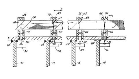
Referring to Figure 1, a backplane 10, which may be a
printed circuit board or other planar member, has a plurality of
circuit cards 12, 14, 16 and 18 mounted on its one face so as to
extend perpendicular to the backplane 10. The circuit cards 12, 14,
16 and 18 are coupled to the backplane by electrical connectors 20,
22, 24 and 26, respectively, adjacent holes 28, 30, 32 and 34,
respectively, which extend through the backplane 10. An optical
conductor 36 is mounted on the opposite face of the backplane 10 by a
set of seating members 38, 40, 42 and 44 spaced apart along its
length, one over each of holes 28, 30, 32 and 34, respectively.
As shown also in Figure 2, each seating member 38, 40,
42 or 44 comprises a block of aluminum having a seatin0 ;n the form of
a square aperture 46 to receive and positiYely locate the optical
conductor or waveguide 36. The optical conductor 36 has a polygonal,
- 15 specifically square, cross-sectional shape and is a close fit in the
~ aperture 46. The facets comprise planar surfaces, at least the
: lowermost one of which accurately locates the conductor 36 with its
bottom facet parallel to the backplane 10. The base of each seating
member 38, 40, 42 or 44 has an anchorage in the form of a set of
spigots 48 (see Figure 2) which project beyond the end oP the seating
: member to engage in corresponding holes 50 ln the backplane 10. The
spigot holes 50 surround the corresponding one of holes 28, 30, 32 and
34 so that each seating member is located over the corresponding one
of holes 28, 30, 32 and 34.
A hole or cavity 51 extends between the square aperture
46 and the anchorage end of the seatlng member 42. A lens 52 is
supported to extend across the hole 51 between the base of square
aperture 46 and the anchorage 48. Each lens 52 is arranged with its
~" .
.
1 2 7 7~L~
optical axis perpendicular to the longitudinal axis of the optical
waveguide 36 and aligned, through the hole 28, 30, 32 or 34, with an
optical element in the form of a receiver 54, 56 or 58 or an optical
transmitter 60 mounted on the corresponding one oF the circuit cards
12, 14, 16 and 18. The optical transmitters may be light-emitting
d;odes and the receivers photodiodes. Each LED or photodiode is
fitted with a lens 53 corresponding to lens 52 (see Figure 1).
Alternatively, ~nd perhaps preferably, lasers could be
used. The LED, photodiode or laser, need not be located immediately
adjacent the backplane but could be positioned some distance away,
poss;bly not even on the circuit card, and connected by means of
another optical conductor or optical fiber, which then constitutes the
transmitter or receiver.
As shown in more detail in Figures 3, 4, 5 and 6, the
optical conductor 36 has a series of reflector means or taps formed by
inclined planar surfaces 62, 64, 66 and 68 aligned with the lenses 52
in seating members 38, 4~, 42 and 44, respectively. The inclined
surfaces 62, 64 and 66 are formed as mitred ends of a series of
; circular cavities 70, 72 and 74, respectively (see Figure 5). The
20 final inclined surface 62 is formed by mitring the ends of the rod 36.
Each cavity 70, 72 or 74 is conveniently formed during moulding of
the optical waveguide 36 by means of a mould insert in the form of an
obliquely truncated round rod which may readily be obtained with the
requlred precision. The inclined reflector surfaces 62, 64, 66 and 68
may be coated with metal, for example gold or aluminum, to maximize
their reflectance. The inclined surface 68 associated with the
transmitter 60 is inclined oppositely to the other inclined surfaces
so that light from the transmitter 60 is reflected through ninety
. . .
,
,
'
~L~7 7~L~4
degrees to travel along the optical waveguide 36 parallel to its
longitudinal axis. At each of the "receiver" inclined surfaces 62, 64
and 66 a portion of the light is reflected, again through ninety
degrees, to pass through the associated lens 52, the backplane 10,
and the receiver's lens 53, to impinge upon the receiver 54, 56 or 58.
The amount of light reflected will depend upon the area of the
inclined surFace relative to the cross-sectional area of the rod.
Typically this will be 2-4%.
The inclined surfaces may be made to have a larger area
the further they are away from the transmitter 60 in order to maximize
the number of taps permitted. Masking or shadowing of one inclined
surface by the preceding one has not been found to be a sign;ficant
problem. The combinat;on of small tap area, large inter-tap spacing,
and multimode transmission serves to ensure that light by-passing one
inclined re~lector surface reaches the next.
It may be convenient for the optical conductor to
receive a light signal from, say, an optical fiber which is behind the
backplane 10. The embodiment of Figure 7 shows a convenient way of
coupling such an optical fiber 80 to the optical conductor 36. The
latter is similar to the optical conductor shown in Figure 3-6, in
that it has a series of reflector surfaces 64, 66 etc. but differs in
that the reflector surface 82 arranged to receive light from the
optical fiber 80 is on the opposite side of the optical conductor 36,
i.e. adiacent the backplane 10. The associated support member 84 has
spigots 86 securing it to the backplane 10, and a lens 88 mounted in a
hole 90 in the part of the support member 84, that is, on the side
away from the backplane 10.
: B
.. . ,, . ~ . . . :
.~ ,. . . .
.
~LZ 7~L6~
The optical fiber 80 is terminated in a connector 92
which houses a second lens 94. The connector 92 fits over the end of
the support member 84 so that the axes of the lenses 88 and 94 are
substantially aligned.
Thus, the light signal can be brought into the cabinet
from the rear, i.e. behind the backplane, as is usual. It is Fed into
the optlcal conductor 36 via the connector 92, lenses 88, 94 and
directed along the optical conductor 36 by the reflector surface 82.
The other reflector surfaces 64, 66 etc. distribute the signal to the
circuit cards as described with respect to Figure 1.
In the practical embodiment illustrated in Figure 8,
four optical conductors 100, 102, 104 and 106 extend parallel to each
other on a backplane-mounted support (not shown). One transmitter and
two receivers are mounted on each of four circuit cards 108, 110, 112
and 114, respectively. The transmitters and receivers are connected
to optical conductors 102 and 104, respectively. Optical conductor
104 is shown coupled at one end (light can, of course, be launched
into these optical conductors through the end~ to a transmitter 116
and is coupled via its reflectors to first ones of the receiver ports
of circuit cards 108, 110, 112 and 114. The other receiver ports are
coupled laterally to the optical conductor 106, which is coupled at
its end to a control/supervisory transmitter 118.
It is preferred for the data signals in the optical
conductors 102, 104 and 106 coupled to the circuit card to travel in
the same dlrection. This simplifies synchronization. Accordingly,
optical conductor 102 ls coupled by a U-bend (actually two 45 deyree
; bends such as disclosed in our copending patent application number
517,834 by D.A. Kahn) to the fourth optical conductor 100, which
' ': ' ' . .
': . ' , : , ,
.
~L~7 7~L6 4
carries the data signals in the opposite direction to the data
receiver 120.
In either the embodiment of Figure 1 or the embodiment
of F;gure 7, it may be preferable for the inclined surface (68 or 82)
- 5 which receives light from the transmitter to be larger than usual, for
example the whole of the oblique cross-sectional area of the
conductor.
Various modifications of the specific embodiments are
possible without departing from the scope of the invention. For
example, the rod may be of other polygonal shapes, such as hexagonal,
triangular or octagonal, and the inclined reflector surfaces may be
provided in the same surface as that from which the light emerges.
In preferred embodiments of the invention, the light
source employs multimodal excitation, specifically with a range of
angles of internal light rays of about 10 degrees. With such
multimodal excitation, the spacing between aligned reflectors need
not be particularly large to avoid shadowing of one reflector by the
preceding reflector. In the exemplary embodiment, the spacing between
the adjacent reflectors was about 50 mm, giving a ratio of reflector
spacing to reflector diameter of about 150:1.
It w-ill be appreciated that although the reflector
surfaces in the specific embodiment will reflect only about 2-4% of
the light travelling along the conductor, -if light is being
transmitted into the waveguide via such surfaces, they will reflect
substantially all of the light. This is mainly because the lens
system enables one to image the source onto the reflector so that
substantially all of the light gets transmitted along the conductor.
The difference is that the transmitted light is still concentrated
E~ .
.~ , ~ . , ~ .
, ' ' .
.
~ L~77~L6 4
into a few modes, whereas the light in the waveguide comprises many
more modes.
Moreover, although the reflector means in the specific
embodiment comprise planar surfaces, other types of reflective
surfaces might be employed, for example the prismatic reflector
surface disclosed and claimed in our copending application number
517,834 by D.A. Kahn, or other means employing total internal
reflection.
An advantage of those embodiments of the invention
which involve a ro~ of reflectors in a straight line in the same
surface of the waveguide, is that masking or "shadowing" of one
reflector is not a s;gn;f;cant problem because of the multimode
transmission in the waveguide.
The specific embodiment comprises a so-called
directional coupler inasmuch as the inclined surface at each tap point
is inclined in one direction only. It is envisaged that a
bidirect;onal coupler could be provided by forming two oppositely-
~ inclined surfaces at each tapping point. Then one would reflect light
- to travel, or travelling in, one direction along the waveguide and the
-~ 20 other would reflect light to travel, or travelling in, the opposite
direction.
Of course, the oppos;tely-incl;ned surfaces might be
spaced apart, perhaps to serve different circuit cards or d;fferent
parts of the same card.
Although c;rcular cavit;es are preferred for ease of
mould manufacture, other shapes are comprehended by the invention; in
particular, square or otherwise rectangular cross-section m;ght be
11
~ B
.
. ~ .
.
.. .. :. .
: . :
3L~2 7 7~LÇi~
preferred because such a tap has maximum efficiency due to minimum
loss of light.
It should be appreciated that the inclined surfaces
may be provided in any combination of orientations to give 1:n
distribution, n:1 concentration or multiplexing, or even n:m, i.e.
plural transmitters to plural receivers.
- . . . .
: :,, ' . , . . . :, ~. .
,' ' '' ' ~,'; ' ~
': .