Note: Descriptions are shown in the official language in which they were submitted.
-" lZ7~3~3
EVENT DISTRIBUTIO~ AND COMBINATION SYSTEM
,.
- - Background of the Invention
The present invention relates in general to
electrical control systems and in particular to an
apparatus for logically combining, synchronizing and
distributing event detection signals for triggering
purposes.
E:lectrical control systems typically employ
sensors to produce digital indicating signals on
detection of various external events. The indica-
ting signals are then logically combined to produce
triggering signals to control triggerable deYices.
Complex systems typically employ many such event
detectors to provide the necessary information to
control many such triggerable devices. Often, how-
ever, it is not possible to locate the event detec-
tors and the trigger circuitry in the same equip-
ment module, such as a circuit board, and in com-
plex systems extensive wiring between equipment
- modules is often required to interconnect event
detecl:ion and trigger control circuitry. Further,
events and triggers are often synchronous signals
within an equipment module, with each module having
its own independent clock, and it is often difficult
to synchronize events and triggers associated with
different modules.
Multiplexing systems have been developed to
reduce the amount of control circuitry whereby
control signals appearing at many locations in one
equipment module have been converted to serial data
for transmission over a single wire pair to remote
; equipment modules. Such multiplexing has besn
effective particularly in reducing int~rpanel
wiring between equipment racks in large control
'~
lZt77;~3
,
systems. -However, parallel-to-seria]. multiplexing
systems typic-ally employ complex circ~itry, do not
lend themseives to interconnecting triggering sig-
nals between small equipment modules and are
unsuitable for high speed operation.
What is needed i5 a means or logically inter-
connecting event detectors and 1:riggerable devices
in a control system which minimizes the amount of
interconnecting wiring and which provides for syn-
chronization of differently clocked events andtriggers.
Summa ry o f the Invention
According to one a pect of the invention, a
control system, comprising sepa;-ate equipment
modules wherein each equipment l~odule contains or
interfaces one or more event detectors, is provided
with one or more event logic un:its which produce a
set of digital output signals o~ states dependent on
logical combinations of input s:ignal5 from the event
detectors. The output signals of the event logic
units are pl~ced on an "interim function bus" com-
prising a set of lines interconnecting each module
in the system in parallel. Each equipment module of
the control system containing or interfacing one or
more triggerable devices is provided with one or
more triggering logic units, each of which produces
a triggering signal of a ~tate dependent on selected
logical combinations of signals occurring on the
lines of the interim function bus. The event logic
units compactly encode event information conveyed by
a large numbex of event indicating signals inko a
parallel code carried between modules on a rela-
tively small parallel bus and the triggering logic
units decode this code to initiate triggering.
7393
.
~ ccording to another aspect o~ thé invention,
each event logic unit and each triggering logic
unit is programmable such that the triggering sig-
nal produced by each triggering logic unit may
result from occurrence of any selected combination
of event detection signals, and such that the
selected combination may be easily changed.
According to still another aspect of the
invention, each circuit module containing an event
or triggering logic unit is provided with a con-
troller for generating signals used to program the
logic units. The controllers on each module are
interconnected by a second bus permitting an opera-
tor to reprogram the event detection and triggering
logic units from a centralized operator interface
device such as a computer terminal.
According to a further aspect of the inven~
tion, each signal from an event detector is delayed
by an event synchronizing circuit prior to applica-
tion to an event logic circuit until the occurrenceof a pulse on a system clock bus. Similarly, the
out?ut of each triggering lo~ic unit is delayed by
a trigger synchronizing circuit until the next
occurrence of a clock pulse from the triggerable
device. This aspect of the invention permits coor-
dination of events and triggering when operation of
equipment modules, events and triggerable devices
are all synchroniæed to different clocks.
It is accordingly an object of the present
3Q invention to provide a new and improved event dis-
tribution and combination apparatus which minimizes
the amount of interconnection wiring needed to
interface event detectors and triggerable devices.
It is another object of the present invention
to provide a new and improved event distribution
~2773~3
and combination apparatus to generate trigger signals on
occurrence of selected combinations of event detection
signals.
It is still another object of the present invention to
provide a new and improved event distribution and combination
apparatus which may be easily programmed and reprogrammed to
produce trigger signals in response to selected combinations
of events.
It is a further object of the present invention to
provide a new and improved event distribution and combination
apparatus for providing synchronization of event detection
signals to a system clock and for providing synchronization of
triggering signals to the clocks of triggerable devices.
It is yet a further object of the present invention to
provide an apparatus for generating a trigger signal in
response to a predetermined set of events, comprising: means
responsive to said events for generating a set of binary event
indication signals, the state of each binary event indication
signal indicating the state of occurrence of a corresponding
event; a programmable encoding circuit for receiving said set
of event indication signals and for generating a set of
parallel event encoding signals, the state of each event
encoding signal comprising a logical combination of the states
of a programmably determined subset of said event indication
signals; a plurality of conductors for carrying said set of
event encoding signals; and a programmable decoding circuit
for generating said trigger signal on detection of a
predetermined pattern of signal statès occurring on a
programmably determined subset of said parallel conductors.
The subject matter of the present invention is
particularly pointed out and distinctly claimed in the
concluding portion of this specification. However, both the
organization and method of operation together with further
advantages and objects thereof may best be understood by
reference to the following description taken in connection
with accompanying drawings wherein like reference characters
refer to like elements.
~L~773~3
4a
Drawinqs
FIG. 1 is a block diagram of an event distribution and
combination system in accordance with the present invention;
FIG. 2 is a block diayram of the enable circuit of FIG.
1;
FIG. 3 is a block diagram of a portion of the
programmable logic device of the event logic unit of FIG. 1;
l~t~73g3
.
FIG! 4 is a block diagram of a.portion bf the
programmable logic device of the trigger logic unit
o`f FIG. I`;-
FIG. 5 is a block diagram of one of the event
synchronizing circuits of FIG. l;
FI~. 6 is a block diagram of the triggersynchronizing circuit of FIG. l, and
FIG. 7 is a block diagram illustrating the
levels of programmability of the event combination
and distribution system of the present invention.
Detailed_Description
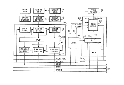
Referring to FIG. 1, an event distribution and
combination system, illustrated in block diagram
form, is adapted to transmit one or more triggering
signals (TRIGGER) to triggerable devices lO in
response to predetermined patterns of input event
indicating signals generated by a set of event
detectors 14 in response to events occurring in
generating devices 12. The present invention
is adapted to minimize the amount of wiring
required to interconnect event detectors 14 and
triggerable devices lO in applications whexe the
event detectors and triggerable devices are mounted
on or accessed through separate equipment modules~
such as circuit~boards. The present invention is
also adapted to synchroni e event detection and
triggering communication between modules when the
modules operate under independent clocks.
The event distribution and combination system
includes one or more event logic units 30 mounted
: on each module receiving event indicating signals
from one or more event detectors 14, and one
trigger logic unit 32 mounted on each module for
each triggerable device 10 accessed by the.module.
:
77393
~ 6
... .
One controller 34 is al~o mounted on each module
containing o~e or more event or t~igger logic
units. All of thé event logic units 30 and trigger
logic units 32 are interconnected in parallel by an
"interim function" bus (IFB) 24 comprising a set of
14 lines for carrying encoded information between
modules.
Each event logic unit 30 monitors the event
indicatlng signals produced by up to ~ix event
- 10 detectors 14 and may be pro~rammed to place prede-
termined patterns of signals on the interim function
bus 24 in response to one or more particular pat-
terns of input event indicating signals. Each trig-
ger logic unit 32 monitors the states of the IFB 24
lines and may be programmed to generate its output
TRIGGER signal on detection of one or more predeter-
mined ~it patterns on the IFB 24. The controllers
34 on each module generate c~ntrol signals applied
to the event logic units 30 and trigger logic units
32. Tl~ese control signals program the pattern
generation and recognition operation of the event
logic units 30 and trigger logic units 32 on the
module. Each controller 34 i5 access~d by another
bus 36 which carries programming data to the con-
troller 34 from an extexnal operator interfacedevice, such as a microcomputer system.
The present invention mini~izes the am~unt Q~
intermodule wiring required to coordinate input
events with output trigger signals by making effi-
cient use of the interim function bus 24. A 14line interim ~function bus is capable of carrying
many different bit patterns. Each event logic
unit 30 can be programmed to produce any one o
these bit patterns in response to particular pat-
terns of input event indicating signals and each
1;~77393
,trigger logic unit 32 may be progra~mméd to produce
a TRIGGER signal in response to any bit pattern on
the interim function bus. By careful prepro-
gramming of the event and trigger logic units, the
event distribution and combination system can coor-
dinate many event/triggering actions involving many
separate equipment modules using only the 14 inter-
connecting lines of the IFB 24.
Each event logic unit 30 comprises six èvent
synchronizer circuits 16 for receiving output sig-
nals from event detectors 14, one programmable
logic device (PLD) 18 for receiving output signals
from the six event synchronizers 16, and fourteen
enable circuits 22, each interposed between one of
the fourteen output terminals of programmable logic
device 18 and one line of the fourteen line IFB 24.
The event synchronizer circuits 16 synchrcnize
event indicating signals to a system clock by
delaying transmission of event indicating signals
to PL~ 18 until receipt of a pulse from the system
clock (CLOCK) signaI which is carried to each event
synchronizer circuit on a system clock line 20.
Clock line 20 may be controlled by any suitable
source of clock pulses of frequency which may be
independent of clocks used to time the operation of
any module, event generator or triggerable device.
PLD 18 transmits a separate binary output
signal to each of fourteen corresponding enable
circuits 22, the state of each output signal being
set in response to the pattern of input signal states
from event synchronizers 16. The relationships
between PLD 18 output signal states input signal
patterns are détermined by control signals on con-
trol lines 38 from controller 34. ~.ach enable
circuit 22 has a single binary output which is
lZ77;~3
.
connected to one of the 14 lines (IFB~ B13) of
the interim function bus 24. Eac~''enable circuit
has four opérating modes and the mode of operation
is controlled by control lines 42 from controller
34. In one ~ode of operation, the enable circuit
produces an output of the same state as its input,
while in a second mode the enable circuit inverts
its input to produce an output. In a third
operating ~ode, the enable circuit 22 ~aintains its
output in a continuously low state regardless of
the state of the input, while in a fourth mode the
enabl~ circuit maintains its output in a contin-
uously high state.
All fourteen lines of IFB 24 are coupled to
programmable logic device 26 of triggering logic
unit 32. Each trigyering logic unit 32 comprises one
programmable logic device ~PLD) 26, having inputs
rece-ving each ~ine of the IFB 24. PLD 26
produces an output signal (TRG) in response to a
particular pattern of input signals from the IF~
24, the pattern being determined by control data on
control lines 40 from controller 34. Each
triggering logic unit 32 also comprises a trigger
synchronizing circuit 28 for receiving the TRG
signal from PLD 26 and for transmitting th~ TRIGGER
signal to the triggerable device 10 in response to
the TRG signal from PLD 16. If triggerable device
10 operation is synchronized to its own clock, the
trigger synchronizing circuit 28 generates the
TRIGGER sign 1 on the leading edge of the first
pulse a clock signal ~CLK) provided by the
triggerable device 10 following detection of the
TRG signal by the synchronizing circui~. If
triggerable device 10 is to operate asynchronously,
an "ASYNC" signal on a control line 37 from
:1~77393
.
controller 34 to the trigger synchronizing circuit
28 causes the synchronizing circuit to immediately
pass the TRG input signal as the TRIGGER signal to
the triggerable device 10 without synchroni~ation
to the CLK signal.
Controller 34 suitably comprises a shift
register and a bus interface! circuit for storing
data from control bus 36 in the shift register.
The shift registex of controller 34 produces a
parallel set of output bits on control lines 37,
38, 40 and 42 after receiving the same set of bits
in serial form ove!r a serial data line of bus 36.
Since the shift register in controller 34 is
loaded one bit at a time as it receives clock
pulses on clock line 20, the control data
applied to each pr~grammable device continuously
changes d~ring reprogramming and each programmable
device passes through a succession of interim
states wherein the device has unintended
input/output relationships which can lead to
generation of unexpected TRG signals. By freezing
- the state of the TRIGGER signal output of each
synchronizing circuit 28 prior to reprogramming the
system, the changes in the TRG signals may be
prevented from inadvertently triggering any
triggerable device. The controller 34 preserves
the state of ~he TRIGGER signal output of each
trigger synchronizing circuit 28 of FIG. l during
reprogram~ing by deasserting a PROGRAM* ~ignal on
control line 39 to the trigger synchronizing cir-
cuit 28, the PROGRAM* signal being continuously
asserted when the system is nst being reprogrammed.
The PROG~AM* signal is carried to each controller
34 by control bus 36 and is forwarded to the
trigger ~ynchronizing circuits on control line 39
by the controller 34.
FIG. 2 ~epicts an enable circui-t 22 of FIG. 1
in more detail. Enable circuit 22 comprises a NAND
gate 40 and an exclusive NOR (XNOR) gate 41. NAND
gate 40 has one input terminal for an output bit
from PLD 18 and has a second input ter~inal for an
ENABLE s.ignal from controller 34 over one of con-
trol lines 42. The output of NAND gate 40 i9
applied to one input of XNOR gate 41 while a SENSE
signal from controller 34 is trans~itted to a second
input of XNOR gate 41 over a second contro:L line
42. The output of XNOR gate 41 is coupled to one
line of IFB 24. If the ENABLE signal from control-
ler 34 is low, the output of NAND gate 40 ~ill be
high, regardless of the state of the input signalfrom DEV 18. Therefore, controller 34 can block
any effect on the enable circuit 22 output due to the
PLD 18 input signal by holding the ENABLE line low.
On the other hand, with the enable line frc,m con-
troller 34 high, the state of the NAND gate 40output will be the inverse of the state of the
input signal from PLD 18.
If both inputs of XNOR gate 41 are the same
logic level (both high or both low), the gate
output is high, while if the two inputs are of
differing logic levels, the XNOR gate output level
is low. If the SENSE signal from controller 34 is
high, then the output state of XNOR gate 41 will be
equal to the 0l2tpUt state of NAND gate 40. If the
SENSE signal from controller 34 is low, XNOR gate
41 will invert the ~utput of NAND gate ~0~ Thus,
depending on the states of the SENSE and ENABLE
control signals applied to enable circuit 22, the
output state of circuit 22 may be equal to the
state of the data input from PLO 18, may be the
llZ77393
inverse of the data input state, or may be high or
low regardless of the state of the ihpUt data.
FIG. 3 depicts a preferred embodiment of a
portion of programmable logic device 18 of FIG. 1.
PLD 18 comprises fourteen ~AND gates 44, each
summing the outputs of a corresponding set of six
enable circuits 21, identical to enable circ~its 22
of FIG. 2. Only one NAND gate 44, and its asso-
ciate~ set of enable circuits 21, are shown in FIG. 3.
Each enable circuit 21 of each set receives the
output of one of the six event signals from syn-
chronizer circuits 16 of FIG. 1, the output of any
one event synchronizer circuit 16 being tied in
common to the input of one enable circuit asso-
ciate~ with each of the fourteen NAND gates 44.Enable circuits 22 perrnit controller 34 to proqram
PLD 1~ by controlling the states of the ENABLE and
SE~SE control lines to each enable circuit 21 such
that each enable circuit 21 may selectively pass,
invert or block -ignals from an associated event
synchronizing circuit 16, selectively applying
either a high or a low voltage to the associated
input of any NAND gate 44 when the event signals
are blocked. Therefore, PLD 18 can be programmed
to produce an output signal of a selected state on
each IFB 24 line on occurrence of any selected
pattern of data signals from synchronizex circuits 16.
Progra~mable logic device 26 of trigger logic
unit 32 of FIG. 1, depicted in more detailed block
diagram form in FIG. 4~ comprises a set of fourteen
enable circuits 23 similar to previously described
enable circuits 22 of FIG. 2, each coupling one line
of IFB 24 to one input of a fourteen input NAND gate
45. The output of NAND gate 45 is applied as one
lnput signal to an XNOR gate 25 while a SENSE control
~73~3
12
8ignal on control line 40 from controller 34 ie
applied to aNother input of the XNOR gate. T~e
output of XNOR ga~e 25 provides the input ~ignal
tTRG) to ~ynchronizing circuit 28. In the ~ame
5 manner as controller 34 uses SENSE and ENABLE ~ig-
nals on lines 42 to program the operation of PLD 18
of FIG. 3, controller 34 can program PLD 26 to
produce a trigger signal of either ~ense on d~tec-
tion of any selected bit pattern on IFB lines by
appropriately setting the 6taltes of the SENSE and
ENA~LE signals on lines 40 aE~plied to enable cir
cuits 23 and XNOR gate 25 of PLD 26.
The preferred embodi~ent cf ~vent synchroni-
.zing circuit 16 of FIG. 1, depicted in more detail
in FIG. 5, comprises RS flip-flop 46, type D flip-
flops 48 and 50, and inverters 52, 54 and 56. RS
flip-flop 46 output Q is set tc~ a high (logical 1)
state when the SET input S of the flip-flop is set
to a low (logical 0) state. Flip-flop 46 output Q
is reset to a logical 0 when the reset input R is
set to a logical 0. D type flip-flops 48 and 50
each produce logical 1 Q outputs and logical 0 -Q
outputs whenever a logical 1 appears at the D input
on the rising edge of a CLOCK Fulse applied to the
T input. If the D input is low during a rising
edge of the CLOCK pulse, the Q output is reset to 0
and the -Q output is reset to 1.
An input signal from event detector 14 of FIG. 1
is applied to the set input of RS flip flop 46. The
Q output of flip-flop 46 is applied to the D input of
flip-flop 48 while the Q output of flip-~lop 48 is
connected to the D input of flip-flop 50. The -Q
output of flip-flop 50 is inverted by inverter
52 and beco~es the synchronizer output 6ignal
to PLD 18 of FIGo 1~ Also, the output of
12~773~3~
13
inverter 52 is in turn inverted b~ inverter 54 and
applied to resét terminal R of Rg flip-flop 45. A
CLOCK signal on clock line 20 is connected to the T
input of flip-flop 48 and the same clock signal is
inverted by inverter 56 and applied to the T input of
flip-flop 50. Therefore flip-flop 48 changes state
only on the rising edge of a clock pulse on line 20,
while flip-flop 50 changes state only on the falling
edge of a clock pulse on line 20.
Assuming that both the set and reset inp~ts of
flip-flop 46 are initially high, that the Q output
is low, that the output of the synchroni~er at
inverter 52 is low, and that the input to flip-
flop 46 from event detector 14 is driven low,
indicating occurrence of an event, then the Q output
of flip-flop 46 latches in high state. On the next
rising edge of a CLOCK pulse on line 20, flip-flop
~8 changes state, driving its Q output high. Then,
on the falling edge of the ne~t pulse on line 20,
flip-flop 50 changes state, driving the -Q output
low. The output of inverter 52 goes high causing
inverter 54 to dxive the inverting reset input of
flip-flop 46 low to reset the Q output of flip-
flop 46 when the inverting set input goes high
again. If the set inpu~ is still low, flip-flop 46
will re~ain set until the set input does go high.
With flip-flop 46 reset, flip-flop 48 resets on the
next leading edge of a system CLOCK pulse, causing
flip-flop 50 to xeset on the falling edg~ of the
: 30 next system CLOCK pulse, thereby driving the event
synchronizing circuit 16 output at invPrter 52 low
again.
Thus flip-flop 46 latches on a signal from an
event detector L4, while the combination of flip- :
flops 48 and 50 synchronizes the transmission of an
:
~L277393
14
event signal to PLD 18 until the st~rt of thé next
CLOCK pulse and ensures that the event signal to
PLD 18 remains high for at least one clock cycle.
The signal from event detector 14 need remain on
only long enough to set flip-flop 46 and the double
~locking of flip-flops 48 and 50 provides protec-
tion against ~etastable input states and provides
synchronization of the event indication to the
syst~m clock.
Trigger synchronizing circuit 28 of FIG. 1,
shown in more detailed block diagram foxm in FIG.
6, comprises type D flip-flops 60 and 62, a
transparent latch 61, a switch 74, and a drivin~
amplifier 64 for producing the TRI~GER siqnal to
triggerable device 10 of FIG. 1. The TRG signal
from the PLD 26 of FXG. 1 drives a D input of
transparent latch 61 while the PROGRAM* signal on
control line 39 from the controller 34 of FIG. 1
controls a G input of latch 61. The transparent
latch 61 transfers the state of the TRG signal at
its D input to its Q output when the G input is high
and freezes the state of the Q output when the G
input goes low. Therefore when the PROGRAM* signal
is deasserted during a system reprogramming opera-
tion, the TRG signal has no effect on the Q outputof latch 61 so that the state of the TRIGGER signal
remains fixed. ~The ASYNC signal from controller 34
controls the switching state of switch 74 which
connects the Q output of latch 61 to the input of
amplifier 64 on assertion of the ASYNC signal on
control line 37, applied as a switching control
input to switch 74. Thus when the triggerable
device 10 of FI&. 1 is to operate asynchronously,
the ASYNC line is asserted and a TRG signal
35. appearing at the Q output of latch 61 is routed
~ 773S~3
imme~iately to the input of amplifier 64 to
initiate the TRIGGER signal output ofithe
amplifier.
The Q output of latch 61 is also connected to
an inverting reset input of flip~flop 60, the D
input of latch 60 ~eing tied to a logic level "1"
source and the T (clock) input of latch 60 being
controlled by the CLK signal from the triggerable
device. The Q output of flip-flop 60 drives the D
input of flip-flop 62 while the CLK signal from
triggerable device 10 controls the T input of flop-
flop 62. Switch 74 connects the Q output of flip-
flop 62 to the input of amplifier 64 when the ASYNC
signal on control line 37 is not asserted and the
triggerable device 10 of FIG. 1 is to be operated
synchronously.
The TRIGGER signal output of amplifier 64 is
intended to trigger a triggerable device as the
TRIGGER signal goPs low. In the synchronous mode
of trigsering, as long as the TRG signal from PLD
26 remains high, the Q outputs of flip-floE,s 60 and
62 remain high, the output of switch 74 remains
high, and the TRIGGER signal remains high. When a
TRG signal from PLD 26 goes low, indicating that
PLD 26 has determined device 10 should be
triggered, flip-flop 60 immediately resets, driving
its Q output low. On the next rising edge of a CLK
pulse from the TRG device/ flip-lop 62 resets,
driving its Q output and the output of switch 74
low causing amplifier 64 to generate the active low
TRIGGER signal to triggerable device lO. As long
as the TRG ~ignal from PLD 26, applied to the rese~
input of flip-flop 60, remains low, trigger yn-
chronizing circuit 28 will continue tG generate a
low TRIGGER signal to the trigge~able device 10.
~;~773~3
1~
On the next CLK pulse rising edge after the T~G
signal from PLD 26 returns to a high state, flip-
flop-60 ~ets. Then, on the next subsequent CLK
- pulse rising edge, flip-flop 62 sets, driving the Q
output of flip-flop 62 high, driving the switch 74
output high, thereby turning off (driving high) the
TRIGGER signal generated by driver amplifier 64.
Therefore, trigger synchronizing circuit 28 ini-
tiates and terminates TRIGGER signals to
triggerable device 10 synchronized with the CL~
pulses from the triggerable clevice when the ASYNC
signal on line 37 is held low.
T~le event distribution and combination system
.of the present invention provides three levels of
prograT~mable logic which enable selected combina-
tion~ of events detected by event detectors 14 to
trigger selected co~binations of triggerable
devices 10 mounted in physically separate component
modules, thereby to reduce the amount of inter~
module wiring. Each level of programmable logic is
designed to accept a plurality of binary inputs and
to prot~uce a single binary output, the state of the
output being determined by any desired combination
of inpl1t states. Generally, each level of progra~-
mable logic includes the equivalent of a ~irstgroup of enable circuits, a NAND or an AND gate,
and an additional enable circuit. Each enable
circuit of the first group receives one input
signal and produces an output signal which may be
programmed to be of the same or inverse logi~ level
to its input signal, or held continuously high or
low regardless of the state of its input signal.
The outputs of the fir~t group are co~bined with a
NAND (or AND) gate and the output of the NAND ~or
AND gate) i5 applied as input to the additional
~2773g3
17
.
enable circuit ~hich produces a sing~e bit oatput.
This arrangement permits any desired pattern of
input signals to trigger a single output signal of
either s~ate.
Referring to FIG. 7, the first level of pro-
grammability (Level 1) comprises each PLD 18 in
each module in combination with the enable circuits
22. Each PLD 18 includes fourteen sets of six
enable circuits 21, one set associated with each
line of the interim function bus. One such set,
associated with bus line IFBO is illustrated in
FIG. 7. Each set of enable circuits 21 receives up
to six event indicating inputs fro~ the event
detectors and the six outputs of the enable circuits
21 are applied as inputs to a NAND gate 44. The
output of NAND gate 44 is applied to the input of
enable circuit 22 which provides the sisnal output
for controlling IFB0. Thus the first level of
programmability is capable of driving each line of
the IFB high or low in response to any desired
combination of input event indicating signal states,
or continuously high or low regardless of states of
the input events.
For convenience, the discussion of the second
level of programmability will follow the discussion
of the third level of programmable logic. The
third level tLevel 3) o~ programmability is pro-
vided by every PLD 26 in the system, each of which
includes a set of fourteen enable circuits 23, each
receiving one of the IFBO-13 lines as inputs, a
NAND gate 45 for receiving the outputs of the
enable circuits 23, and an XNOR gate 25 for
receiving the output of the N~ND gate 45 and for
producing the TRG signal. In an alternative embo-
diment of the present invention, another NAND gate
.
~m3~3
18
47 (shown in dotted line) is inserte~ between theoutput of NAND gate 45 to provide ena~le condi-
tioning of the output of NAND gate 45 such that
NAND gate 47 and XNOR gate ~S comprise a complete
enable circuit. With NAND gate 47 in place, PLD 26
can produce a TRG signal of state determined by any
combination of states on the IFB0-13 lines or (when
the enable signal to NAND gal:e 47 is held low) which
is continuously high or low regardless of the state
10 of the IFB lines. However, this can be done by deas-
serting all of the enable signal inputs to enable cir-
cuits 23. Therefore, NAND gate 47 is omitted from
the PLD 18 in the preferred embodiment of the
invention without reduction in utility.
The second level (Level 2) of programmability
has all of the outputs of Level 1 as its inputs and
produces all of the inputs to Level 3 as its out-
puts. Each Level 2 output is of a state which may be
determined by the states of a selected combination
of several Level 1 outputs, or may be held con-
tinuously high or low. In an alternative embodi-
ment of the invention, Level 2 programmability is
provided by a set of enable circuits 84, each
receiving the output of one enable circuit 22 of
one module 30. The ou~puts of the enable circuits
84 are provided as inputs to an AND gate 88, and
the output of AND gate 88 is connected to an input
of an enable circuit 90. The output of enable
circuit 90 drives one of the IFB lines, in the
example case, IFB0. Thus the second level of pro-
grammability can set the s~ate of any one of the
IFB lines according to any combination of Level 1
output states from modules 30 or can set the IFB
line continuously high or low regardless of the
module 30 output states. However since each enable
~277393
lg
circuit 22 is connected in series wlth an enable
clrcuit 84, no loss of programming flexibility
occurs when the enable circuit 84 is bypassed
because enable circuit 22 can be programmed to
produce any de~ired input to AND gate -88 in
response to the output of NAND gate 44 which could
be produced by enable circuits 22 and 84 is seri~s.
By a similar argument, enable circuit 90 ca~ also
be eliminated without loss of programming flexi-
bility since it is in series with enable circuit23. Finally, AND ~3ate 88 is eliminated in the
preferred embodiment of the invention because the
open collector outputs of enable circuits 22 can be
directly connected to the IFB, thereby providing a
"hardwired" AND of these outputs. Thus while Level
2 programmability exists in the preferred embodi-
ment of the invention and provides additional
flexibility in relating events to triggering
signals, the second level of programmability is
provided without additional hardware ~y accounting
for the lack of enable circuits 84 and 90 in the
programming of enable circuits 22 and 23 and by
hardwire ~N~ing the outputs of enable circuits 22
onto the IFB bus lines.
With the three levels of programmable logic,
the system may be programmed with flexibility to
independently trigger many triggerable devices 10
upon occurrence of many possible combinations of
eventst within limits generally determined by the
size of IFB 24. As IFB 24 lines are increased in
number the number of separately distinguishable bit
patterns which can be simultaneo~sly transmitted by
IFB 24 also increases, permitting more devices to
be independently triggered at the same time.
It should be noted that Level 1 m2y be
~Z7~393
bypassed in alternative embodiment~ of the inven-
tion by coupling the output of each of the event
synchronizers 18 to the interim function bus
through a separate enable circuit 22. Similarly,
Level 3 may be omitted by connecting selected lines
of IFB 24 directly to the inputs of trigger syn-
chronizing circuits 28. In either case triggerable
device 10 may be triggered on any combination of
signals from event detectors 14. However inclusion
- 10 of Level 1 and Level 3 programming permits an
increase in the efficiency of use of IFB 24 and in
the flexibility of the system in permitting simul-
taneous triggering upon occurrence of many separate
event combinations.
Thus, in addition to providing synchronization
between event and triggering signals, the ~-vent
distribution and combination system of the present
invention minimizes the amount of wiring needed to
interconnect event detectors and triggerable
devices mounted in separate component modules by
providing a relatively small interface bus to inter-
connect the modules, and three levels of programma-
bility for efficiently encoding and decoding
triggering data carried on the interface bus. In
the preferred embodiment of the in~ention, separate
~ equipment modules are mounted in a common mainframe
: : and the interim function bus is provided as back
` plane wiring interconnecting the modules. Since
the:maximum length o~f interim function bus 24 which
can be utilized to interconnect separate equipment
~ modules is limited when~high frequency operation is
; required, it is usually preferable to provide a
separate event distribution and combination system,
including a sepa:rate interface bus within each
35- mainframe of a multiple-frame system and to provide
~.z~
21
a set of TRIGGER signal outputs fro~ ~ach mainframe
as event signal inputs to the other ~ainframes.
The unidirectional TRIGGER qignals are more ~asily
adapted for long distance transmission than the bi~
directional IFB bus signals and since each TRIGGER
signal output of a mainframe can represent any
selected combination of event inputs to the mai~-
frame, a group of TRIGGER signals transmitted to
another mainframe can be encoded to efficiently
carry triggering information between mainframes in
much tne same way that the IFB bus is encoded to
efficie~ntly carry trig~ering information between
modules within a mainframe. Thus the present
invention is easily adapted for efficiently com-
municating event information between mainframas aswell as between modules within a single mainframe.
W~ile a preferred embodiment of the present
invention has been shown and described it will be
apparent to those skilled in the art that many
change; and modifications may be made without
departing from the invention in its broader
aspects. For example, while ths prefer~ed embodi-
ment of the invention is intended for use with a
fourteen line interim function bu 24, other embodi-
ments of the invention may employ other numbers ofIFB lines. Similarly, while eve11t signals are
applied to each PLD 18 in groups of six, other
group sizes are possible. The appended claims are
therefore intended to cover all such changes and
modifications as fall within the true spirit and
scope of the invention.
;