Note: Descriptions are shown in the official language in which they were submitted.
iZ'77A35
~ Description
Chip Contacts Without Oxide Discontinuities
Background of the Invention
The present invention relates generally to metal
contact layers for integrated circuit chips, and more
particularly to such metal contact layers which are
devoid of opens and direct shorts to semiconductor.
The deposition of conductive material over a
topography which includes an abrupt vertical step
frequently results in opens or shorts through to the
underlying semiconductor. Such opens or shorts cause
significant declines in chip yield. Unfortunately,
such vertical steps are common throughout most chips
due to the need to etch through insulator layers
overlying chip devices to make electrical contact
thereto. Such problems are particularly severe where
the sidewalls of the abrupt steps overhang a portion of
the bottoms of the steps. Attempts have been made to
avoid these opens and shorts by using tantalum or
tungsten silicides as the wiring layer. However, such
silicides have too much electrical resistance,
resulting in significant heat generation. Accordingly,
tantalum or tungsten silicide wiring is unacceptable
for dense bipolar chip applications.
Other approaches to this problem have centered
around using wide metal bands and a series of
intermediate steps in place of one abrupt step.
However, these approaches use a significant amount of
chip real estate, thereby limiting chip device and
circuit density.
The invention as claimed provides a structure and a
method for eliminating shorts and opens in the contacts
made through one or more insulator layers to electrical
devices and circuit elements therebelow.
FI9-87-022 -1-
'
~277~3~
SummarY of the Invention
Briefly, the present invention comprises an
integrated circuit chip, includiny
a first surface at a first approximate level;
a second surface at a second different level
approximately parallel to the first surface;
a subs$antially abrupt transition between the first
surface and the second surface, including a sidewall;
a first layer of a first conductive material
disposed over the first surface and disposed over the
second surface, but terminating on the first surface in
a first end portion which extends up to but does not
touch the sidewall, the first layer having a thickness
of less than the difference between the first and
second levels,
wherein the end portion of the first layer of
conductive material has been converted to an insulator;
and
a second layer of a second conductive material
disposed on top of the first layer, with essentially no
conductive material conversion to insulator therein
adjacent to the abrupt transition.
In one embodiment of the present invention, the
first layer disposed over the second surface has a
second end portion disposed at an edge of the second
surface above the abrupt transition, and wherein the
second end poxtion of the first layer of conductive
material has been converted to insulator.
A further feature of the present invention is that
there is a region of the first layer adjacent to the
insulator end portion which has a lower material
density than the bulk of the first layer.
In yet a further embodiment of the present
invention, the insulator-converted end portion of the
first layer on the first surface adjacent to the abrupt
transition and the insulator-converted end portion of
the first layer on the second surface adjacent to the
abrupt transition meet to form a continuous insulator
FI9-87-022 -2-
seam along the abrupt transition. This continuous
insulator seam has a length which is less than fifty
percent of the total combined thickness of the first
and second layers.
If only one end portion is formed in the contact,
it is preferred that this insulator-converted end
portion have a length which is less than thirty-three
percent of the total combined thickness of the first
and second layers. Typically, this insulator-converted
end portion will have a length rising from the first
surface in the range of 900 - 1800 Angstroms.
In one embodiment of the present invention, the
conductive material for the first and second layers may
be an alloy of aluminum and the end portions may
comprise species of aluminum oxide.
The present invention further comprises a method
for forming the inventive structure disclosed
previously. This method comprises the steps in a
processing chamber of
providing oxygen in the atmosphere of the
processing chamber;
depositing a first conductive layer on to a step to
a first thickness which is less than the height of the
step, with the first layer terminating in an end
portion on the lower level of the step below the step
overhang, but not touching the base of the step, the
depositing step being performed at a first temperature
and a first rate chosen to insure maximum gettering of
undesired elements and to insure that the end portion
of the first conductive layer is converted to an
insulator;
depositing a second conductive layer to a thickness
which is at least three times the thickness of the
first layer with a deposition temperature which is
initially ramped from the first temperature to a second
temperature which is at least fifty percent greater
than the first temperature and at a higher second rate
relative to the first rate so that conversion of the
FI9-87-022 -3-
~27743~
second conductive layer to insulator is minimized.
In a preferred embodiment, the first temperature is
less than 125 and preferably on the order of 100C.
The first rate is preferably less than 6 Angstroms per
second, and the second rate is greater than 15 - 20
Angstroms per second.
Brief Description of the Drawings
Fig. 1 is representation of a complete oxide seam
through a conductive layer that will lead to an open
circuit failure.
Fig. 2 is a cross-sectioned diagram of a step at a
collector contact formed in accordance with the present
invention.
Fig. 3 is a cross-sectioned diagram of a step at an
emitter or a Schottky barrier diode contact formed in
accordance with the present invention.
Detailed Description of the Preferred Embodiment
.
The present invention will be described and
discussed in the context of covering steps for
collector, emitter, and Schottky barrier diode
' contacts. ~owever, the present invention is not
limited thereto, but has wide applicability to any
situation wherein an abrupt step must be covered by a
conductive material.
Referring now to Fig. 1, there is shown a
representation of a conductive contact to a
semiconductor device which is prone to failure. With
reference to the Figure, the layer 10 will typically be
some form of insulator material such as silicon dioxide
or silicon nitride disposed over a semiconductor or
conductor material 19 therebelow. This layer 10 will
have an abrupt or reentrant step 18 formed therein in
order to facilitate contact with the semiconductor or
conductor material 19. A layer 14 of conductive
material is provided for forming the contact. A layer
12 of a barrier metallurgy is provided for preventing
FI9-87-022 -4-
~277~
the penetration of the contact metal layer 14 through
to the semiconductor layer 19. It can be seen fro~ the
Figure that there is a vertical insulator seam 16 which
occurs right at the abrupt step 18 for the structure.
In a typical embodiment, the conductive Contact metal
layer 14 may be an alloy of aluminum, i.e., AlCu, and
the insulator seam 16 may comprise aluminum oxide.
ThiS aluminum oxide seam 16 is electrlcally resistive
and subject to high stresses. Localized heating of
this seam during later process steps causes
differential expansion of materials, causing the oxide
to open, resulting in device failure.
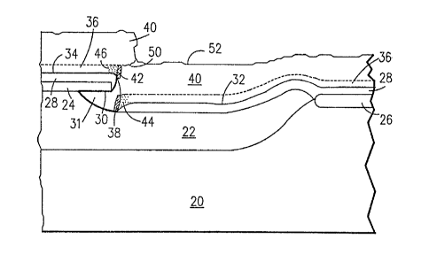
Referring now to Fig. 2, there is shown one
embodiment of the present invention. Fig. 2
lS illustrates a profile of a step at a collector contact
for a device formed therebelow in the chip. In this
example, the area 20 comprises either doped or undoped
semiconductor material such as, for example, silicon.
The layer 22 is a recessed oxide insulator layer, and
may be typically comprised of silicon dioxide. The
layer 24 may comprise silicon nitride. The layer 26
may comprise platinum silicide. The layer 28 may
'' comprise a typical barrier metallurgy for preventing
the conductive material of the contact from penetrating
to the semiconductor layer 20. It can be seen from a
review of the Figure that there is a substantially
abrupt transition or step 30 in the topography of the
layers. Such steps are typically in the range of 2000
- 8000 Angstroms. The top surface 32 of the barrier
layer 28 to the right of the abrupt transition step 30
comprises a first surface at a first approximate level.
Likewise, the top surface 34 of the barrier layer 28 to
the right of the abrupt transition step 30 comprises a
second surface at a second different level
approximately parallel to the first surface.
A first layer 36 of a first conductive material is
disposed over the first surface 32 and over the second
surface 34. This first layer 36 disposed over the
FI9-87-022 -5-
~Z77435
first surface 32 terminates in a first end portion 38
adjacent to but not touching the abrupt step sidewall
step 30. This first layer has a ~,hickness of less than
the difference betwee~ the first and second levels.
The first end portion 3~ of the first layer of
conductive material has been converted to an insulator.
A second layer 40 of a second conductive material is
disposed on top of the first layer 36, with essentially
no conductive material conversion to insulator adjacent
to the abrupt transition.
In many applications, the process used to form the
abrupt step to make electrical contact to the device
therebelow comprises an etching process which has a
tendency to undercut laterally as it etches downward.
Accordingly, the sidewall for the abrupt transition 30
is typically angled to overhang a portion of the first
layer 36, such that the first end portion 38 of the
first layer 36 terminates under the sidewall overhang.
In some embodiments of the present invention, that
portion of the first layer 36 disposed over the second
surface 34 will have a second end portion 42 disposed
at an edge of the second surface 34 above the abrupt
" step transition 30, with the second end portion 42 of
the first layer of conductive material being converted
to an insulator.
In some embodiments of the present invention,
regions 44 and 46 of the first layer 36 adjacent to the
respective first and second insulator end portions 38
and 42 have a lower material density (more porosity3 as
compared to the bulk of the conductive material of the
first layer 36.
In one embodiment of the present invention, the
first and second conductive material layers 36 and 40
may be aluminum alloys such as alloys of aluminum and
copper. A typical barrier layer 28 which may be
utilized to prevent the penetration of the aluminum
through to the semiconductor 20 is a Cr/Cr203 "cermet"
mixture. For aluminum alloy layers 36 and 40, the
FI9-87-022 -6-
~Z7~ ~3 ~
first and second end portions 38 and 42 may be
conveniently converted to an insulator such as aluminum
oxide.
In some embodiments of the present invention where
the first and second conductive materials in the layers
36 and 40 are the same material, the second conauctive
material layer 40 will have a greater density than the
first conductive material layer 36, prior to sintering.
In a preferred embodiment, when only the first
insulator-converted end portion 38 is present, this end
portion should have a length which is less than
thirty-three percent of the total combined thickness of
the first and second conductive layers 36 and 40. In
embodiments where each of the first and second
insulator-converted end portions 38 and 42 are present,
then each of these end portions should have a length
which is less than twenty-five percent of the combined
total of the lengths of the first and second layers 36
and 40. In a preferred embodiment, each of these
insulator-converted end portions may have a length in
the range of 900 - 1800 Angstroms.
It can be seen from a review of Fig. 2 that there
will be a good coverage area 50 in the second
conductive layer 40 in every instance, which will
guarantee that there are no continuous vertical seams
of insulator or continuous vertical voids extending
from the bottom of the step, i.e., surface 32, to the
top surface 52 of the second layer 40. This structure
thus insures that there will be no opens or shorts for
this contact, despite the abrupt step topography being
covered.
Referring now to Fig. 3, there is shown a profile
of an emitter or a Schottky barrier diode contact step.
Again, it should be noted that the present invention is
not limited to emitter or SBD contacts, but is
applicable wherever an abrupt step occurs in the device
topography. In the example shown in Fig. 3, an area 60
typically comprises some form of semiconductor
F~9-87-022 -7-
12774~i
material. For emitter contacts~ the semiconductor
material below the trench step is typically highly
doped An insulator layer 62 is disposed over a
portion of the semiconductor material 60, and may be,
for example, an insulator such as silicon dioxide or~
CVD glass to a thickness of 800 Angstroms. Likewiser :a
layer 64 disposed over the insulator 62 may be a sec~nd
insulator layer of, for example, silicon nitride to a
thickness of 1600 Angstroms. A layer of material 66 ~t
the bottom of the step may again be platinum silicid~.
Finally, a layer 68 disposed over the layers 64 and
may comprise a barrier material such as Cr/Cr203 to
thickness of 1600 Angstroms. An abrupt step 71 is
formed in these layers in order to facilitate contact
to the semiconductor material 60 disposed therebelow.
Again, depending on the etching process utiliæed to
form the step 71, the abrupt transition for the step
may overhang a void area 70 therebelow.
The present invention again comprises the disposal
of a first layer 36 of a first conductive material ove~ ~`
the first and second surfaces 32 and 34, respectively
Again, a second conductive layer 40 is disposed ove~ ;-`i
the first conductive layer 36. However, in this
embodiment because the difference in levels between t~e - ~-
first and second surfaces 32 and 34 is not as great a~ ~
the difference in levels for the collector contact, the ~!
fir3t and second end portions meet to f~rm a continuo~s
insulator seam 72 which follows the abrupt transition
step 71. The length for this continuous insulator seam
72 should have a length which is less than 50% of the
total combined thickness of the first and second laye~s
36 and 40. Again, this first layer 36 will have
regions 74 adjacent to the insulator end portion seam
72 which have a lower material density as compared to
the bulk of the first layer 36. In one embodiment, t~e
materials for the first and second conductive layers ~6
and 40 may be an alloy of aluminum and the insulator
seam may be aluminum oxide.
FI9-87-022 -8-
~27743S
It should be noted again that there is a
substantial "good" coverage area 50 wherein no
conductive material in the second layer 40 has been
converted to insulator adjacent to the abrupt
transition 71. This structure thus insures an absence
of opens and shorts at this step transition for the
contact.
A process for forming a conductive layer over an
abrupt step between a first and second levels on the
surface of an integra~ed circuit chip will now be
~ described. With reference to Fig. 2, it should be
noted that the deposition of the various semiconductor,
insulator, and metal layers 20, 2Z, 24, 26, and 28 are
well known in the art and will not be discussed in this
disclosure. For further information on the deposition
of these layers, please refer to the reference article
by Fried, Havas, Lechaton, Logan, Paal, and Totta, IBM
Journal of Research and Development, Vol. 26, No. 3,
May 1982. The process for the present invention takes
place in a chamber and comprises the steps of providing
an oxygen source in the atmosphere of the processing
chamber; depositing a first conductive layer to a first
' thickness which is less than the height of the step,
with the first layer terminating in an end portion on
the lower level of the step up to but not touching the
base of the step, with the depositing step being
performed,at a first tem?erature and a first rate
chosen to insure maximum gettering of undesired
elements and to insure that the end portion of the
first conductive layer is converted to an insulator.
The method further comprises the step of depositing a
second conductive layer to a thickness which is at
least three times the thickness of the first layer,
with a deposition temperature which is initially ramped
from the first temperature to a second temperature
which is at least fifty percent greater than the first
temperature, and at a higher second rate relative to
the first rate, so that conversion of portions of the
FI9-87-022 -9-
~Z7743~;
second conductive layer to insulator is minimi~ed.
In one embodiment of the present invention, a
standard processing chamber such as the type
manufactured by Temescal or Balzer may be utilized.
The first step of providing an oxygen source in the
atmosphere of the processing chamber may be
accomplished simply by venting the chamber to air or
backfilling the chamber with N2O. In some processes,
H20 is put into the chamber for a water bleed step
during the deposition of the barrier metal layer 28.
This H20 may then comprise a source of oxygen in the
chamber. The chamber may then be pumped down to 2 x
10 6 Torr.
The next step is the first layer depositing step.
It is preferred that this deposition step be at a first
temperature of less than 125C. However, the
temperature to be used will depend on the conductive
material being deposited in this step. For the
deposition of AlCu, a temperature of less than 125 and
typically on the order of 100C is preferred. This low
temperature deposition may be accomplished by
directional low temperature processes such as
evaporation at approximately vertical incidence on to
the surface. The deposition rate for this first layer
should be on the order of 6 Angstroms per second or
less, with a preferred range of 3 - 5 Angstroms per
second. This low depositio~ rate and low temperature
produces a condition for maximum gettering of oxygen
during the initial stages of the deposition. This low
temperature and low rate deposition also provides a
reduced conductor atom mobility during the deposition
process, which results in the creation of a porous, low
density network of the conductor metal, with many voids
at the edges of the first layer. The end portions 38
and 42 shown in Fig. 2 have this porous, low density
network structure. Such structure directly facilitates
the oxidation of these end portions. In the example
where the first layer material is an aluminum alloy,
FI9-87-022 -10
127743~i
then these end portions 38 and 42 are oxidi~ed to an
insulator which is a species of aluminum oxide. This
aluminum oxide end portion or collar extends around the
entire perimeter of the contact hole and acts as a
diffusion barrier to metal "creep" or migration, thus
preventing me~al penetration. Typically, this end
portion collar around the perimeter of the contact hole
is disposed underneath the overhang of the sidewall of
the step 30. This insulator end portion or collar 38
prevents any metal diffusion or migration into the
active semiconductor region during any subsequent
thermal cycle for the chip.
It should be noted that the voids or mouseholes 31
disposed below the overhangs provide a significant
amount of surface area for the absorption of oxygen and
water vapor. This absorption enhances the formation of
the aluminum oxide at the end portions 38 adjacent to
these voids or mouseholes. It has be theorized that
the majority of oxygen utilized to oxidize the first
conductive layer end portions 38 and 42 is coming from
water vapor let into the processing chamber during
venting. The reduction of the deposition temperature
` for this first conductive layer 36 to significantly
less than the boiling point of water decreases the
amount of water vapor that will be desorbed from the
contact microstructure. This availability of oxygen in
combination with the reduced mobility of the aluminum
atoms during deposition due to the lower temperature,
significantly enhances the creation of the aluminum
oxide end portions.
Typically this first layer 36 will be deposited to
a thickness in the range of 800 - 1600 Angstroms.
The next step in the process comprises depositing a
second conductive layer 40 to a thickness which is at
least 3 times the thickness of the first layer, with a
deposition temperature which is initially ramped from
the first temperature to a second temperature which is
at least fifty percent greater than the first
FI9-87-022 -11-
~Z7743~;
temperature, and at a higher second deposition rate
relative to ~he first rate. By way of example, this
second deposition step may be initiated after 900
Angstroms of the first layer 36 have been deposited.
In a preferred embodiment, the high deposition rate
for this step is not initiated until the substrate has
been raised to the proper temperature. Since it
generally takes longer to raise the substrate
temperature, a temperature ramp of, for example, 40 -
50 seconds is ~egun prior to initiation of the high
deposition rate. Accordingly, the temperature in the
processing chamber may be initially ramped to on the
order of 180 C or greater. For example, a ramp rate of
50C in one minute may be utilized. This temperature
ramping within the chamber may be accomplished by
utilizing the backside heaters present in typical
tools. During this second deposition step, the
pressure within the chamber in the example for the
deposition of aluminum is maintained at 2 x 10⁻⁶ Torr.
After approximately 100 Angstroms have been
deposited during this second deposition step, the
deposition rate is ramped to a rate in the range of 10
- 30 Angstroms per second. A preferred rate for
aluminum deposition might be 20 Angstroms per second
ramped at a rate of 40 seconds 110 seconds. The
deposition of this second layer 40 is continued at this
second higher te~mperature and higher deposition rate
until a desired thickness of 7000 - 10000 is achieved
for this second layer. It should be noted that during
this second layer deposition period the temperature may
continue to increase by a certain amount. For example,
the temperature may initially be ramped to a second
temperature of 180C and continue to increase to a
temperature of 200C at the end of this second
deposition step. During this second deposition step,
good vacuum conditions of on the order of 2 x 10⁻⁶ Torr
should be maintained. A Meisner trap may be utilized
to maintain the desired pressure. Note that any tool
FI9-87-022 -12-
~27743~;
outgassing is accomplished via gettering during the
first layer deposition step at the low temperature.
Any excess gasses are then trapped by the Meisner
system attachments.
At the end of the process, the shutter from the
target is turned off, the substrate heaters are turned
off, the power to the electron gun is turned off, and
the rotation of the dome is stopped. The substrate is
vacuum cooled for 2 - 5 minutes. Then the chamber is
soft-vented.
It should be noted that this high temperature
second layer deposition provides the conductor atoms
being deposited with a sufficient mobility so that a
higher density second conductor layer is obtained.
This second conductor layer is not porous and does not
contain the low density network of voids which
facilitates oxidation of the structure.
From the above, it can be seen that a conductive
layer deposition process has been disclosed which
significantly increases wafer yield and satisfactory
reliability by eliminating open collector and open
emitter problems and preventing Schottky voltage
degradation. This process is particularly advantageous
for obviating the shadowing effects of nitride during a
barrier metal deposition. Such shadowing limits the
ability of the barrier metal vapor stream to
effectively cover the contact edges of the material
which it is protecting. This process may be
advantageously used with a wide variety of deposition
processes and is particularly advantageous with
directional low-temperature evaporation and sputtering
(where there is a high sticking coefficient). The
present structure and process are specifically designed
to prevent the formation of vertical insulator seams
which run from the top of a conductor layer down to the
bottom of a step. Such seams are particularly prone to
occur along vertical steps during prior art processes
with the occurrence of air leaks or when water vapor is
FI9-87-022 -l3-
~2'77~3~;
bled into the system.
While the present invention has been particularly
shown and described with reference to the preferred
embodiments therefor, it will be understood by those
skilled in the art that the foregoing and other changes
in form and detail may be made therein without
departing from the spirit and the scope of the present
invention, as defined in the appended claims.
FI9-87-022 -14-