Note: Descriptions are shown in the official language in which they were submitted.
774~
- 7261
Title; DUAL LAYER ENCAPSULATION COATING FOR III - V
SEMICONDUCTOR COMPOUNDS
BACKGROUND OF THE INVENTION
. . .
1. Field of the Invention
This invention relates generally to a method of
providing a dual layer masking or encapsulation coating
for a III - V compound semiconductor substrate and for
providing metallized contacts therefor and, more
- particularly, to a method for providing dual layers of
silicon and silicon nitride to operate as a mask or
encapsulation coating for a III - V compound semiconductor
substrate and for thereafter applying metallized contacts
to the III - V compound semiconductor substrate.
20 Description of the Prior Art
It is well known in the art to use silicon
dioxide or silicon nitride coatings as a dielectric dif-
- 15 fusion mask coating for III - V compound semiconductors.
However, the coef~icent of thermal expansion or these
coatings may differ substantially depending upon the
deposition conditions from that of the III - V compound
semiconductors thereby resulting in problems associated
with interfacial stress or cracking of the coatings during
thermal treatment. The silicon dioxide or silicon nitrlde
coatings may be deposited on the III - V semiconductor
compounds using a high temperature chemical vapor deposi-
tion (CVD) or a low temperature plasma enhanced chemical
vapor deposition ~PECVD) process. In the high temperature
chemical vapor deposition process, the temperatures
--1--
requir~d to achieve the requisite chemical reactions are
o~ten in the order of 700 C to 1,000 C. III - V com-
pound semiconductors such as gallium arsenide and indium
phosphide thermally decompose at such temperatures result-
ing in one or more components from the decomposed III - V
compound being incorporated in the silicon dioxide or
silicon nitride coating. The semiconductor properties are
altered and the unwanted components of the III - V
compound semiconductor may thereafter affect subsequent
device processes such as the application of metallized
contacts.
The alternate (PECVD) procedure for depositing
dielectric mask coatings on III - V compound semi-
conductors offers the primary advantage of the ability to
grow the dielectric mask coatings at relatively low
temperatures usually well under 300 C. However, this
advantage is offset by the loss in the compositional con-
trol of the dielectric material. The coatings may be
randomly bonded, highly cross linked in a variable
composition. Chemical species other than the desired ones
are often included in the dielectric mask coatings. Thus,
in (PECVD) films, a range of stoichiometry is possible
depending on the plasma and operating conditions; and this
variation in the stoichiometry generally results in
undesirable variations in electrical, mechanical and
chemical properties of the deposited dielectric mask
coating leading to poor coating characteristics such as
bubbling or cracking.
As a result of these problems, silicon coatings
have been used for diffusion masks for III - V compound
semiconductors. Silicon coatings, composed of only a
single element, are inherently more reproducible. Silicon
coatings generally match the thermal coefficients of
expansion of the III - V compound semiconductors thereby
providing rea~onably good performance as a diffusion
--2--
d~
- mask and encapsulation coating. However, diffic~lties
arlse whe~ the silicon coatings are subsequently
metallized during device processing ~s a result of the
formation of silicides which ~ay be detrimental to device
operation.
Therefore, it is a primary object of this
invention to provide an improved diffusion mask or
encapsulation coating for use with III - V compound
semiconductors.
It is a further object of this invention to
provide a dual layer mask or encapsulation coating for use
with III - V compound semiconductors that maintains the
dual advantages of relative impermeability to metalliza-
tion and the closely matched coefficients of thermal
; 15 expansion o~ silicon and III - V compound semiconductors.
Other objects of the invention will be, in part,
obvious and will, in part, appear hereinafter. The
.
invention accordingly comprises a mechanism and system
- possessing the construction, combination of elements and
- 20 arrangement of parts which are exemplified in the
following detailed disclosure.
SUMMARY OF THE INVENTION
A process for providing a mask or encapsulation
coating over the exterior surface of a III - V compound
semiconductor comprises the first step of depositing a
- layer of silicon to a select thickness over the exterior
surface of the III - V compound semiconductor utilizing a
deposition temperature not to exceed the congruent
evaporation temperature of the III - V compound
semiconductor. A second step comprises depositing a layer
; of silicon nitride to a select thickness over the exterior
- surface of the silicon layer. The silicon layer is
deposited preferably by electron beam evaporation and the
silicon nitride layer is deposited preferably by plasma
enhanced chemical vapor deposltion. A process for
'
~743~
providing a metallized contact to the III - V co~pound
semiconductor having the aforementioned Coating Comprises
first defining a s~lect area to ~etch on the outside
surface of the silicon nitride layer by masking the areas
on the outside surface of the silicon nitride layer not to
be etched. The silicon nitride layer is thereafter
reactive ion etched in the areas selectively defined by
masking in the aforementioned step. The silicon ~ayer is
thereafter plasma etched in the same areas and titanium
and gold are electron beam evaporated in seque~ce to
overlay the etched areas of the III - V compound
semiconductor. The titanium and gold are thereafter heat
treated to provide an alloy of titanium and gold.
DESCRIPTION OF THE DRAWINGS
The novel features that are considered
characteristic of the invention are set forth with
particularity in the appended claims. The invention
itself, however, both as to its organization and its
method of operation, together with other objects and
advantages thereof will be best understood from the
following description of the illustrated embodiment when
read in connection with the accompanying drawings wherein-
FIG. 1 is a cross-sectional view of a portion of
a III - V compound semiconductor having the dual layer
coating of this invention;
FIG. 2 is a cross-sectional view of the III - V
compound substrate of FIG. l to which a photoresist has
been applied~
FIG. 3 is a cross-sectional view of a portion of
the I~I - V compound of FIG. 2 which has been selectively
etched in the manner of this invention;
FIG. 4 is a cross-sectional view of a portion of
a III - V compound of FIG. 3 to which zinc has been
diffused;
~4.~3~3
FIG, 5 is a cross-sectional view of a portion ~f
the III - V compound of FIG. 4 to which a metallized
coating has been applied; and
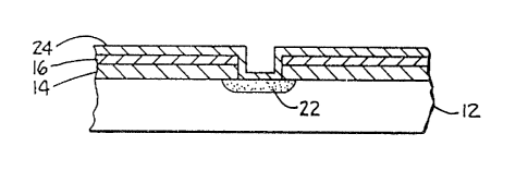
FIG. 6 is a cross-sectional view of a portion of
the III - V compound of FIG. 5 in which the metallized
coating has been selectively etched to define a specific
metallized contact.
. DESCRIPTION OF THE PREFERRED EMBODIMENT
Referring now to FIG. 1, there is shown a III
V compound semiconductor substrate 12 overlayed in the
manner of this invention with dual masking or
encapsulation layers 14 and 16. III - V compounds are
typically binary, ternary and quaternary compounds
composed of elements from the III and V columns of the
periodic table including gallium arsenide, indium
phosphide, etc. Prior to application of the masking or
encapsulation layers 14~ 16 in the manner of this
invention to be herein described, the III - V compound
substrate 12 is degreased or solvent cleaned as ~ollows.
Substrate 12 is first soaked for two minutes in
trichloroethane, followed by a two minute soaking in
~ acetone, followed by a two minute soaking in methanol.
- After being soaked, the III - V compound substrate 12 is
then blow dried in nitrogen on filter paper. Any oxide
that may have formed on the surface of the III - V
compound substrate 12 is subsequently remove~ by soaking
the substrate in a one to two mixture of hydrofluoric acid
and water for thirty seconds followed by a thirty second
rinse with deionized water. The substrate 12 is
subsequently blow dried in nitrogen on filter paper.
The first masking or encapsulation layer 14 is
applied by E beam evaporating silicon using a Temescal
FC-1800 system. The E-beam evaporation is carried out by
first loading a high purity carbon crucible with silicon
pellets and then evaporating the silicon at a rate of six
-5
~X77~3~
to eight angstroms per second und~r a pressurc o~
approximately 1.2 microtorr. The substrate 12 can be
heated to a temperature in the range of 150 C to 300 C
during the evaporation process, and the silicon coating 14
is deposited to a preferred thickness of 1,000 angstroms.
The temperature range to which the substrate is heated
does not exceed the congruent evaporation temperature of
the III - V compound semiconductor. Although the
preferred thickness for the silicon layer 14 is 1,000
angstroms, acceptable thicknesses may be in the range of
150 angstroms to 5,000 angstroms.
The next succeeding layer 16 is applied by the
plasma enhanced chemical vapor deposition (PECVD) of
silicon nitride using a Plasma-Therm Model PK 1432 PD
system. The (PECVD) process is accomplished in a chamber
pressurized to 650 millitorr. Ammonia gas is directed
into the chamber at a flow rate of five standard cubic
centimeters per minute, silane gas is directed into the
chamber at a flow rate of 390 standard cubic centimeters
per minute, and nitrogen gas is directed into the chamber
at a flow rate of 700 standard cubic centimeters per
minute. The chamber includes an upper electrode which is
preferably maintained at a temperature of 60 C and a
lower electrode which is preferably maintained at a
temperature of 220 C under a radio frequency (RF) power
of 10 watts. The silicon nitride is preferably deposited
to a thickness of 200 angstroms although an acceptable
range of thickness is 150 angstroms to 5,000 angstroms.
In order to deposit the silicon nitride layer to the
preferred 200 angstrom thickness, the plasma enhanced
chemical vapor deposition must be maintained for a period
of 3.2 minutes.
A photoresist 18 is applied in a well-known
manner as shown in FIG. 2 to define selected openin~s, one
of which is shown at 20. The silicon and silicon nitride
layers 14, 16 are thereafter etched in the area
immediately adjacen~ the opening 20 using a Plasma-Therm
dual chamber etch system (Model No. 520/540). The silicon
5 nitride layer 16 is etched in a chamber maintained at a
pressure o~ 20 millitorr inko which oxygen is directed at
a f low rate of 5 standard cubic centimeters per minute,
and carbontetrafluoride is directed at a flow rate of 20
standard cubic centimeters per minute. The radio
frequency ~RF~ power iS ~aintained at 50 watts for 45
seconds to reactive ion etch ~lle silicon nitride layer 16
as shown in FIG. 3. In order to therea~ter etch ~he
silicon layer 14, the chamber iS repressurized to 350
millitorr, and oxygen is directed therein at a flow rate
lS of two standard cubic centimeters per minute, and
carbontetrafluoride is directed therein at a flow rate of
40 stan~ard cubic centimeters per minute. The radio
frequency ~RF) power is maintained at 150 watts for
preferably six minutes to plasma etch the silicon layer 14
as shown in FIG . 3 .
A zinc diffusion step may thereafter be carried
out in a well-known manner in a Pacific Western diffusion
furnace using gallium arsenide/zinc arsenide (GaAs/Zn2As3)
source material to provide the zinc diffusing region 22 as
shown at FIG. 4. The zinc diffusion is preferably con-
ducted at a temperature of 650 C for three hours although
an acceptable range of zinc diffusion temperatures are
from 300 C to 900 C within a time range of 30 minutes to
lO0 hours.
A metallized layer as shown at 24 is deposited
by the E-beam evaporation of titanium/gold using a
Temescal FC-1800 system. The titanium is deposited by
evaporating titanium pellets loaded in a high purity
carbon crucible at a rate of 5 angstroms per second under
-7-
a pressure of 1.2 microtorr. The titanium is preferably
coated to a thickness of 250 angstroms, although an
acceptable range of thicknesses is between 150 angstroms
and 1,000 angstroms. The gold is evaporated from gold
S pellets loaded in a high purity carbon crucible at an
evapo~ation rate of 10 angstroms per second under a
pressure of less than 1.2 microtorr. The gold is
preferably coated to a thickness of 2.5 kiloangstroms but
may have an acceptable range of thicknesses of 1.5 kilo-
angstroms to 10 kiloangstroms. The gold and titaniumlayers are thereafter alloyed by heat ~reatment at 420D C
for one minute in a conventional strip heater alloy
station. Acceptable alloy temperatures are in the range
of 300 C to 700 C, while acceptable alloying times are
in the range of 15 seconds to 60 minutes. The alloy
titanium and gold layer is thereafter selectively removed
to provide the contact 24' as shown in FIG. 6 by
well-known photoresist and etching techniques.
Thus, in this manner there is provided the dual
layer maskin~ or encapsulation coating of this invention
comprising the silicon layer 14 which substantially
matches the thermal coefficient of expansion of the III -
V compound semiconductor substrate and a silicon nitride
layer 16 which is substantially impermeable to the
absorption of the metallized contact 24'. In addition,
the color of the silicon nitride layer 16 substantially
contrasts with the color of the III - V compound
semiconductor substrate 12 thereby facilitating mask
alignment subsequent to etching.
Other embodiments of the invention including
additions, subtractions, deletions and other modifications
of the preferred disclosed embodiments of the invention
will be obvious to those skilled in the art and are within
the scope of the following claims.
--8--