Note: Descriptions are shown in the official language in which they were submitted.
~. ~7769~
THERMAL FUSE
BACK'~ G~
Field of the Invention
This invention relates to thermal fuses and, in
particular, to a form of thermal fuse for use in electronic and
similar circuits.
Related Art
In electronic devices, components are mounted on, or
formed as part of, a conductive circuit pattern. Such a circuit
pattern may be formed on a surface of a circuit board or on a surface
of a ceramic or other substrate. To protect the components, it is
desirable to provide some means for opening the circuit if an overload
occurs.
~ MM~
The present invention provides a thermal fuse in which
a fusible alloy forms a conductive path through the fuse under normal
; conditions, with the fusible alloy melting and opening the circuit
when the thermal fuse reaches a predetermined temperature.
In its broadest concept, a thermal fuse comprises a
thin member having at least one electrical path therethrough, filled
with a fusible alloy, with connections made to each end of the path.
In particular, the path is formed between two plates of ceramic
material. The ceramic plates can be in a green form when put
together, the path defined by a material capable of being removed when
the ceramic plates are fired~ During firing, the ceramic plates fuse
together, except when the removable material is positioned. AFter
~ ~7~95
removal of the material, the path is filled with a fusible alloy.
Other ways of forming the paths can be used.
BRIEF DESCRIPTION OF THE DRAWINGS
The invention will be readily understood by the
following description of certain embodiments, by way of example, in
conjunction with the accompanying drawings, in which:
Figure 1 is a plan view on a substrate with three paths
defined;
Figure 2 is an end view of the substrate in Figure 1;
Figure 3 is an end view of the substrate in Figure 1,
with a further member placed thereon, the substrate and member of
green ceramic;
Figure 4 is a similar view to that of Figure 3, prior
to firing,
Figure 5 is a cross-section on the line V-V of Figure
4, after firing with spacer material in position;
Figure 6 is a view similar to Figure 4, but after
firing;
Figure 7 is a cross-section on the line VII-VII of
Figure 6;
Figure ~ is a cross-section as in Figure 7, but with a
fusible alloy in position,
Figure 9 is an end view of an alternative form of
structure; and
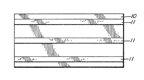
Figure 10 is a plan view oF a substrate showing a
different form of path.
7~76 9 ~
DETAILED_DESCRIPTION OF THE PREFERRED EMBODIMENTS
Illustrated in Figures 1 and 2 is a substrate 10, in
the example ceramic, with three stripes 11 formed on one surface. A
typical example of the material forming the stripes 11 is carbon. The
stripes can be formed by screen printing or otherwise depositing a
carbon ink on the surface of the substrate. As illustrated in Figure
3, the cover member 12 is positioned on the substrate 10~ over the
stripes 11. The substrate and cover are of green ceramic, that is,
ceramic in an unfired condition. Pressing the cover and substrate
together causes them to deform round the stripes until they are in
contact. This is illustrated in Figure 4 and in Figure 5.
The assembly is then fired. During firing, the ceramic
cover and substrate become fused together either side of the stripes.
Also, usually at the same time, the material forming the stripes burns
out to leaYe open channels 15, as illustrated in Figures 6 and 7. A
typical temperature range for firing is 1500 to 2000C.
The channels 15 are then filled with a fusible alloy to
form conductive paths, indicated at 16 in Figure 8. The ends of the
assembly can be metallized as at 17 in Figure 8, to produce contact
areas. The metallization makes contact with the conductive paths 16.
Generally, the assembly is cut into strips with one channel to each
strip, to form a fuse, as indicated by dotted lines 18 in Figure 6.
However, assemblies with more than one channel can be provided.
Figure 9 is an end view of an alternative arrangement
! 25 for forming channels. In this embodiment9 substrate 20 has ribs 21
formed on one surface, the ribs defining three channels 22. A cover
member 23 is positioned on the substrate and the two fused together at
769 ~
,
the top surfaces of the ribs, at 24. This defines channels into which
a fusible alloy is filled to form conductive paths. The substrate can
be of ceramic, formed in its green state and then fired to form the
channels. The cover can also be of ceramic.
The dimensions of a fuse can vary, but one particular
example is about 120 mil by 60 milO The thickness of the substrate
can vary. One exemplary thickness is 10 mil. The stripe or stripes
can be about 1/2 to 1 mil thick. Instead of ceramic, other forms of
dielectric can be used. Thus, a synthetic resin plastic material
~; 10 having a high temperature characteristic can be used. With such a
material, the substrate can be channelled to define the paths and a
top cover will be bonded into position. Both the substrate and the
cover can be channelled with the channels aligned to define the paths.
If both the substrate and the cover are channelled, with the channels
offset relative to each other, then two separate path arrangements can
be provided.
While in the examples described and illustrated
straight paths extending from one end of the substrate to the other, a
path may take a sinuous or zigzag or other form. Figure 10 is a plan
view on a substrate 10 in which a zigzag pattern 30 has been formed
which will eYentually form a zigzag path.
The fusible alloy material is filled into the channels
under pressure in a liquid state. The channels are not completely
filled, a very thin layer of air extends over the alloy material when
it solidifies. The alloy material can vary in composition, depending
upon the temperature at which it is desired that the alloy will melt,
a typical temperature being about 250C. On melting, the alloy will
7~7~9~
break up into isolated sections and thus break the circuit through the
fuse.
The form of the fuse can vary, as can also the
dimensions. A fuse can be mounted by insertion into spring contact
members, for easy replacement~ Alternatively, it can be mounted on a
circuit board by soldering. Other forms of contact member can be
proYided at each end, including leaded contact members. Fuse members
may be mounted on tape or other means for automated placement.
Several fuse members can be formed as a single unit, and can also be
formed integral with some other component. A number of fuse members
can also be formed by superimposing several substrates, forming a
multilayer assembly. One or more conductive, fusible, paths can be
formed between each pair of substrates.