Language selection

Search

Patent 1277715 Summary

Third-party information liability

Some of the information on this Web page has been provided by external sources. The Government of Canada is not responsible for the accuracy, reliability or currency of the information supplied by external sources. Users wishing to rely upon this information should consult directly with the source of the information. Content provided by external sources is not subject to official languages, privacy and accessibility requirements.

Claims and Abstract availability

Any discrepancies in the text and image of the Claims and Abstract are due to differing posting times. Text of the Claims and Abstract are posted:

  • At the time the application is open to public inspection;
  • At the time of issue of the patent (grant).
(12) Patent: (11) CA 1277715
(21) Application Number: 547307
(54) English Title: RADIO BROADCAST COMMUNICATIONS SYSTEMS
(54) French Title: SYSTEME DE RADIOCOMMUNICATION
Status: Deemed expired
Bibliographic Data
(52) Canadian Patent Classification (CPC):
  • 325/41
(51) International Patent Classification (IPC):
  • H04L 27/18 (2006.01)
  • G06K 17/00 (2006.01)
  • H04L 5/14 (2006.01)
(72) Inventors :
  • STEVENS, JOHN KING (Canada)
  • WATERHOUSE, PAUL INGRAM (Canada)
(73) Owners :
  • STEVENS, JOHN KING (Canada)
  • TELEPANEL INC. (Canada)
(71) Applicants :
  • STEVENS, JOHN KING (Canada)
  • WATERHOUSE, PAUL INGRAM (Canada)
(74) Agent: GOWLING WLG (CANADA) LLP
(74) Associate agent:
(45) Issued: 1990-12-11
(22) Filed Date: 1987-09-18
Availability of licence: N/A
(25) Language of filing: English

Patent Cooperation Treaty (PCT): No

(30) Application Priority Data:
Application No. Country/Territory Date
06/909,548 United States of America 1986-09-22

Abstracts

English Abstract


ABSTRACT OF THE DISCLOSURE

The invention comprises a low power broadcast system
that is applicable especially to the so-called "electronic
shelf" for retail stores, wherein the shelf edge carries price
displaying modules that can be addressed and controlled from a
central computer operated station. The system also permits the
modules to broadcast back to the central station to confirm safe
receipt of data and to give information as to stock levels,
etc. A broadcast system avoids the need for wiring so that
location changes are facilitated. To overcome the extremely
noisy environment and to conserve power consumption, and hence
battery life, the system employs a low frequency (132 kHz)
reference carrier transmitted by the base station in discrete
segmented packages, each of which frames a base data word
transmitted by the base station and a corresponding module data
word transmitted by the module a fixed period after the end of
the base word; the base receiver then has precise time
information for receipt of the module word and can "look" for it
among the noise. The carrier received by the module is divided
and the lower frequency used to demodulate the information-
carrying transmission from the base station of the same
frequency, avoiding the need for a phase locked loop detector;
this lower frequency is also used for the module transmission.
The module employs an air-cored loop antenna coil for the lower
frequency and a ferrite-cored loop antenna for the higher
reference frequency, while the store antenna is segmented for
selection of the group of modules to be addressed; the antenna
contacts the metal shelving to provide electromagnetic coupling
thereto. Each module contains a microprocessor which controls
the operation. Each module has "concealed" buttons which can be
enabled and used to insert data to be transmitted therefrom. A
charging circuit can be used as the power source employing the
received RF carrier energy.


Claims

Note: Claims are shown in the official language in which they were submitted.


WE CLAIM:

1. A signal broadcast system comprising a broadcast
transmitter and at least one broadcast receiver, the system
comprising:
means for generating at the transmitter a first carrier
of a first reference frequency N and for broadcasting that first
carrier;
means for generating at the transmitter a second
carrier of second frequency N/n derived from the first reference
carrier where the divisor n is greater than 1, for modulating
the second carrier with a digital modulating signal in
accordance with digital information to be transmitted thereby,
and for broadcasting the digitally modulated second carrier;
means at the receiver for receiving the first carrier
and for dividing it by the divisor n to produce a corresponding
demodulating signal of frequency N/n; and
a demodulator at the receiver receiving the second
digitally modulated carrier and the demodulating signal and
demodulating the second digitally modulated carrier with the
said demodulating signal to generate a resulting digital
information signal.


2. A system as claimed in claim 1, wherein the said second
carrier is phase modulated by the digital modulating signal.


3. A system as claimed in claim 1, wherein the digital

modulating signal is a coded binary signal, and the said second

- 40 -

carrier is phase modulated by the coded binary digital
modulating signal.


4. A system as claimed in any one of claims 1 to 3,
wherein the said first frequency N is in the range 10 kHz - 500
kHz.


5. A system as claimed in any one of claims 1 to 3,
wherein the divisor is an even whole number integer.


6. A system as claimed in any of of claims 1 to 3, wherein
the said first frequency N is in the range 10 kHz - 500 kHz and
the divisor is 2.


7. A system as claimed in any one of claims 1 to 3, and
comprising with each receiving means a visible display unit
receiving the digital information signal and displaying
information thereof.


8. A system as claimed in any one of claims 1 to 3,
wherein the said receiver also comprises means for generating a
second carrier of reference frequency N/n and for transmitting
said carrier, and the said transmitter also comprises receiving
means for receiving the said second carrier from the receiver,
and wherein the receiver in transmitting mode employs the said
second carrier of frequency N/n modulated by the transmitted
signal.


-41-

9. A system as claimed in any one of claims 1 to 3,
wherein the said receiver also comprises means for generating a
second carrier of reference frequency N/n and for transmitting
said carrier, and the said transmitter also comprises receiving
means for receiving the said second carrier from the receiver,
and wherein the receiver in transmitting mode employs the said
second carrier of frequency N/n modulated by the transmitted
signal, and comprising with each receiving means a visible
display unit receiving the digital information signal and
displaying information thereof.


10. A system as claimed in any one of claims 1 to 3,
wherein the transmitter is a base transmitter and also comprises
receiving means for receiving said second carrier, and the
receiver is a module receiver and also comprises means for
generating a second carrier of frequency N/n and for
transmitting said carrier, wherein the said first carrier is
generated at the base transmitter and transmitted therefrom in
the form of sequential discrete envelopes; the base transmitter
when transmitting generates a base data word to be transmitted,
modulates the second carrier therewith and transmits the
resultant modulated second carrier within the respective
envelope;
the receiving means at the module receiver detects the
base data word and in response to its termination generates a
timing period interposed between the received base data word and
an associated module data word to be transmitted by the module
receiver; and

- 42 -


the transmitting means at the module receiver modulates
the second carrier with the module data word and transmits the
resultant modulated second carrier at the termination of the
timing period.


11. A system as claimed in any one of claims 1 to 3,
wherein the transmitter is a base transmitter and also comprises
receiving means for receiving said second carrier, and the
receiver is a module receiver and also comprises means for
generating a second carrier of frequency N/n and for
transmitting said carrier;
wherein the said first carrier is generated at the base
transmitter and transmitted therefrom in the form of sequential
discrete envelopes;
the base transmitter when transmitting generates a base
data word to be transmitted, modulates the second carrier
therewith and transmits the resultant modulated second carrier
within the respective envelope;
the receiving means at the module receiver detects the
base data word and in response to its termination generates a
timing period interposed between the received base data word and
an associated module data word to be transmitted by the module
receiver;
the transmitting means at the module receiver modulates
the second carrier with the module data word and transmits the
resultant modulated second carrier at the termination of the
timing period,


- 43 -


the module receiver receives the said first carrier in
the form of the said sequential discrete envelopes; and wherein
the lengths of each base and respective module data word and the
interposed timing period are such that the module data word
terminates with a respective received first carrier envelope so
that both the base and module data words are framed thereby.


12. A system as claimed in any one of claims 1 to 3,
wherein the transmitter is a base transmitter and also comprises
receiving means for receiving said second carrier, and the
receiver is a module receiver and also comprises means for
generating a second carrier of frequency N/n and for
transmitting said carrier;
wherein the said first carrier is generated at the base
transmitter and transmitted therefrom in the form of sequential
discrete envelopes;
the base transmitter when transmitting generates a base
data word to be transmitted, modulates the second carrier
therewith and transmits the resultant modulated second carrier
within the respective envelope;
the receiving means at the module receiver detects the
base data word and in response to its termination generates a
timing period interposed between the received base data word and
an associated module data word to be transmitted by the module
receiver;
the transmitting means at the module receiver modulates
the second carrier with the module data word and transmits the
resultant modulated second carrier at the termination of the
timing period;

- 44 -

wherein the module receiver receives the said first
carrier in the form of the said sequential discrete envelopes;
wherein the lengths of each base and respective module
data word and the interposed timing period are such that the
module data word terminates with a respective received first
carrier envelope so that both the base and module data words are
framed thereby;and
wherein the receiving means of the transmitter detects
in a received second carrier modulated by a module data word the
leading edge of each module data word at the end of the
respective timing period following the termination of the
corresponding transmitter data word by reference to the
transmission within the time period of the respective discrete
envelope of the respective base data word and the respective
timing period.


13. A system as claimed in any one of claims 1 to 3,
wherein the transmitter is a base transmitter and also comprises
receiving means for receiving said second carrier, and the
receiver is a module receiver and also comprises means for
generating a second carrier of frequency N/n and for
transmitting said carrier;
wherein the said first carrier is generated at the base
transmitter and transmitted therefrom in the form of sequential
discrete envelopes;
the base transmitter when transmitting generates a base
data word to be transmitted, modulates the second carrier
therewith and transmits the resultant modulated second carrier
within the respective envelope;

- 45 -


the receiving means at the module receiver detects the
base data word and in response to its termination generates a
timing period interposed between the received base data word and
an associated module data word to be transmitted by the module
receiver;
the transmitting means at the module receiver modulates
the second carrier with the module data word and transmits the
resultant modulated second carrier at the termination of the
timing period;
and comprising with each receiving means a visible
display unit receiving the digital information signal and
displaying information thereof.


14. A signal communication system comprising a base
transmitter including transmitting means and also including
receiving means, and comprising a plurality of module receivers,
each of which includes a respective receiving means and also a
respective transmitting means;
the transmitting means of the base transmitter
including means for generating a first carrier of a first
reference frequency N and for transmitting that first carrier
respectively to the receiving means of the module receivers;
each transmitting means of the base transmitter and the
module receiver also including means for generating when
transmitting a second carrier of second frequency N/n derived
from the first reference carrier, where the divisor n is greater
than 1, means for modulating the respective second carrier with
a respective digital modulating signal in accordance with

- 46 -

digital information to be transmitted respectively from the base
transmitter and the module receivers, and means for transmitting
the digitally modulated second carrier therefrom;
dividing means at each receiving means receiving the
first carrier from the respective transmitting means and
dividing it by the divisor n to produce a corresponding
demodulating signal of frequency N/n; and
a demodulator at each receiving means receiving the
respective second digitally modulated carrier and the
demodulating signal and demodulating the second digitally
modulated carrier with the demodulating signal to generate a
resulting digital information signal.


15. A system as claimed in claim 14, wherein the said
second carrier is phase modulated by a digital modulating signal.


16. A system as claimed in claim 14, wherein the said
second carrier is phase modulated by a coded binary digital
modulating signal.


17. A system as claimed in any one of claims 14 to 16,
wherein the said first frequency N is in the range 10 kHz - 500
kHz.


18. A system as claimed in any one of claims 14 to 16,

wherein the divisor is an even whole number integer.


- 47 -

19. A signal communication system as claimed in any one of
claims 14 to 16, and comprising with each receiving means a
visible display unit receiving the digital information signal
and displaying information thereof.


20. A signal communication system comprising a base
transmitter including transmitting means and also including
receiving means, and comprising a plurality of module receivers,
each of which includes a respective receiving means and also a
respective transmitting means;
the transmitting means of the base transmitter
including means for generating a first carrier of a first
reference frequency N and for transmitting that first carrier
respectively to the receiving means of the module receivers,
wherein the said first carrier is generated at the base
transmitting means and transmitted therefrom in the form of
sequential discrete envelopes;
each transmitting means of the base transmitter and the
module receiver also including means for generating when
transmitting a second carrier of second frequency N/n derived
from the first reference carrier, where the divisor n is greater
than 1, for generating a data word to be transmitted thereby,
means for modulating the second carrier with the said data word,
and means for transmitting the resultant modulated second
carrier therefrom;
dividing means at each receiving means receiving the
first carrier from the respective transmitting means and
dividing it by the divisor n to produce a corresponding
demodulating signal of frequency N/n; and

- 48 -


a demodulator at each receiving means receiving the
respective second digitally modulated carrier and the
demodulating signal and demodulating the second digitally
modulated carrier with the demodulating signal to generate a
resulting data word;
the receiving means at each module receiver detecting
each received data word and the module receiver in response to
its termination generating a timing period of length such that
the sum of the length of the received data word, the length of
the timing period and the length of a module data word to be
transmitted by the module transmitting means is equal to the
length of a respective envelope of said first carrier frequency;
the transmitting means at the module receiver
modulating the respective second carrier with its data word to
be transmitted and transmitting the resultant, modulated second
carrier at the termination of the said timing period.


21. A system as claimed in claim 20, wherein the broadcast
transmitter in receiver mode detects the leading edge of the
module data word at the end of said timing period following the
termination of the broadcast transmitter data word by reference
to the transmission of the base data word and the timing period.


22. A system, as claimed in claim 20, wherein the said
second carrier is phase modulated by a coded binary digital
modulating signal.


- 49 -

23. A system as claimed in any one of claims 20 to 22,
wherein the said first frequency N is in the range 10 kHz - 500
kHz.


24. A system as claimed in any one of claims 20 to 22,
wherein the divisor is an even whole number integer.


25. A system as claimed in any one of claims 20 to 22,
wherein the said second carrier is phase modulated by a digital
modulating signal.
26. A system as claimed in any one of claims 20 to 22, and
comprising with each receiving means a visible display unit
receiving the digital information signal and displaying
information thereof.


27. A system as claimed in any one of claims 1 to 3, and
for the operation of a plurality of said broadcast receivers
comprising radio receiving shelf-mounted modules by
data-containing signals from the broadcast transmitter
comprising:
at least one metal shelf unit comprising a plurality of
horizontal metal shelves each having an outer longitudinal edge;
a plurality of said broadcast receivers each having a
respective broadcast receiving antenna and each mounted on a
respective shelf outer longitudinal edge; and
the broadcast transmitter having a broadcast
transmitting antenna transmitting radio signals to be received
by the said broadcast receivers;

- 50 -

wherein said broadcast transmitter antenna comprises
an antenna segment for each shelf unit, the respective antenna
segment lying upon a surface of the respective shelf unit
parallel to the said shelf longitudinal edges of the unit for
electromagnetic coupling with the shelf unit and the production
of a corresponding increased field signal strength at the shelf
longitudinal edges to be received by the broadcast receivers
mounted thereon.


28. A system as claimed in any one of claims 1 to 3, and
for the operation of a plurality of said broadcast receivers
comprising radio receiving shelf-mounted modules by
data-containing signals from the broadcast transmitter
comprising:
at least one metal shelf unit comprising a plurality of
horizontal metal shelves each having an outer longitudinal edge;
a plurality of said broadcast receivers modules each
having a respective broadcast receiving antenna and each mounted
on a respective shelf outer longitudinal edge; and
the broadcast transmitter having a broadcast
transmitting antenna transmitting radio signals to be received
by the said broadcast receivers;
wherein said broadcast transmitter antenna comprises
an antenna segment for each shelf unit, the respective antenna
segment lying upon a surface of the respective shelf unit
parallel to the said shelf longitudinal edges of the unit for
electromagnetic coupling with the shelf unit and the production
of a corresponding increased field signal strength at the shelf

- 51 -

longitudinal edges to be received by the broadcast receivers
mounted thereon, and wherein each broadcast receiver is mounted
on a shelf with its antenna disposed vertically, and each
antenna segment produces a magnetic transmission field in the
vertical plane.


29. A system as claimed in any one of claims 1 to 3, and
for the operation of a plurality of said broadcast receivers
comprising radio receiving shelf-mounted modules by
data-containing signals from the broadcast transmitter
comprising:
at least one metal shelf unit comprising a plurality of
horizontal metal shelves each having an outer longitudinal edge;
a plurality of said broadcast receivers each having a
respective broadcast receiving antenna and each mounted on a
respective shelf outer longitudinal edge; and
the broadcast transmitter having a broadcast
transmitting antenna transmitting radio signals to be received
by the said broadcast receivers;
wherein said broadcast transmitter antenna comprises
an antenna segment for each shelf unit, the respective antenna
segment lying upon a surface of the respective shelf unit
parallel to the said shelf longitudinal edges of the unit for
electromagnetic coupling with the shelf unit and the production
of a corresponding increased field signal strength at the shelf
longitudinal edges to be received by the broadcast receivers
mounted thereon, and wherein each antenna segment lies upon the
top surface of the respective shelf unit.

- 52 -


30. A system as claimed in any one of claims 1 to 3, and
for the operation of a plurality of said broadcast receivers
comprising radio receiving shelf-mounted modules by
data-containing signals from the broadcast transmitter
comprising:
at least one metal shelf unit comprising a plurality of
horizontal metal shelves each having an outer longitudinal edge;
a plurality of said broadcast receivers each having a
respective broadcast receiving antenna and each mounted on a
respective shelf outer longitudinal edge; and
the broadcast transmitter having a broadcast
transmitting antenna transmitting radio signals to be received
by the said broadcast receivers;
wherein said broadcast transmitter antenna comprises
an antenna segment for each shelf unit, the respective antenna
segment lying upon a surface of the respective shelf unit
parallel to the said shelf longitudinal edges of the unit for
electromagnetic coupling with the shelf unit and the production
of a corresponding increased field signal strength at the shelf
longitudinal edges to be received by the broadcast receivers
mounted thereon, and wherein the transmitter transmits at a
frequency in the range 10 kHz - 500 kHz.


31. A system as claimed in any one of claims 1 to 3,
wherein the transmitter is a base transmitter and also comprises
receiving means for receiving said second carrier, and the
receiver is a module receiver and also comprises means for


-53-


generating a second carrier of frequency N/n and for
transmitting said carrier, wherein the said first carrier is
generated at the base transmitter and transmitted therefrom in
the form of sequential discrete envelopes; the base transmitter
when transmitting generates a base data word to be transmitted,
modulates the second carrier therewith and transmits the
resultant modulated second carrier within the respective
envelope;
the receiving means at the module receiver detects the
base data word and in response to its termination generates a
timing period interposed between the received base data word and
an associated module data word to be transmitted by the module
receiver; and
the transmitting means at the module receiver modulates
the second carrier with the module data word and transmits the
resultant modulated second carrier at the termination of the
timing period, wherein immediately successive sequential
envelopes are transmitted spaced at predetermined minimum time
periods between them.


32. A system as claimed in any one of claims 1 to 3,
wherein the transmitter is a base transmitter and also comprises
receiving means for receiving said second carrier, and the
receiver is a module receiver and also comprises means for
generating a second carrier of frequency N/n and for
transmitting said carrier, wherein the said first carrier is
generated at the base transmitter and transmitted therefrom in
the form of sequential discrete envelopes; the base transmitter

- 54 -

when transmitting generates a base data word to be transmitted,
modulates the second carrier therewith and transmits the
resultant modulated second carrier within the respective
envelope;
the receiving means at the module receiver detects the
base data word and in response to its termination generates a
timing period interposed between the received base data word and
an associated module data word to be transmitted by the module
receiver; and
the transmitting means at the module receiver modulates
the second carrier with the module data word and transmits the
resultant modulated second carrier at the termination of the
timing period;
wherein the module receiver transmitted data word
comprises in succession data bits and check sum bits.


33. A system as claimed in any one of claims 1 to 3,
wherein the transmitter is a base transmitter and also comprises
receiving means for receiving said second carrier, and the
receiver is a module receiver and also comprises means for
generating a second carrier of frequency N/n and for
transmitting said carrier, wherein the said first carrier is
generated at the base transmitter and transmitted therefrom in
the form of sequential discrete envelopes; the base transmitter
when transmitting generates a base data word to be transmitted,
modulates the second carrier therewith and transmits the
resultant modulated second carrier within the respective
envelope;


-55-

the receiving means at the module receiver detects the
base data word and in response to its termination generates a
timing period interposed between the received base data word and
an associated module data word to be transmitted by the module
receiver; and
the transmitting means at the module receiver modulates
the second carrier with the module data word and transmits the
resultant modulated second carrier at the termination of the
timing period;
wherein the base tansmitter transmitted data word
comprises in succession data bits and check sum bits and the
timing of the said period commences at the trailing edge of the
final data bit.


34. A system as claimed in any one of claims 1 to 3,
wherein the transmitter is a base transmitter and also comprises
receiving means for receiving said second carrier, and the
receiver is a module receiver and also comprises means for
generating a second carrier of frequency N/n and for
transmitting said carrier, wherein the said first carrier is
generated at the base transmitter and transmitted therefrom in
the form of sequential discrete envelopes; the base transmitter
when transmitting generates a base data word to be transmitted,
modulates the second carrier therewith and transmits the
resultant modulated second carrier within the respective
envelope;
the receiving means at the module receiver detects the
base data word and in response to its termination generates a

- 56 -

timing period interposed between the received base data word and
an associated module data word to be transmitted by the module
receiver; and
the transmitting means at the module receiver modulates
the second carrier with the module data word and transmits the
resultant modulated second carrier at the termination of the
timing period;
wherein the base transmitter transmitted data word
comprises in succession password bits, data bits and check sum
bits.


35. A system as claimed in any one of claims 1 to 3,
wherein the transmitter is a base transmitter and also comprises
receiving means for receiving said second carrier, and the
receiver is a module receiver and also comprises means for
generating a second carrier of frequency N/n and for
transmitting said carrier, wherein the said first carrier is
generated at the base transmitter and transmitted therefrom in
the form of sequential discrete envelopes; the base transmitter
when transmitting generates a base data word to be transmitted,
modulates the second carrier therewith and transmits the
resultant modulated second carrier within the respective
envelope;
the receiving means at the module receiver detects the
base data word and in response to its termination generates a
timing period interposed between the received base data word and
an associated module data word to be transmitted by the module
receiver; and

- 57 -

the transmitting means at the module receiver modulates
the second carrier with the module data word and transmits the
resultant modulated second carrier at the termination of the
timing period;
wherein the base transmitter transmitted data word is
transmitted at a first higher BAUD rate and the module receiver
transmitted data word is transmitted at a second slower BAUD
rate.


36. A system as claimed in any one of claims 1 to 3,
wherein the transmitter is a base transmitter and also comprises
receiving means for receiving said second carrier, and the
receiver is a module receiver and also comprises means for
generating a second carrier of frequency N/n and for
transmitting said carrier, wherein the said first carrier is
generated at the base transmitter and transmitted therefrom in
the form of sequential discrete envelopes; the base transmitter
when transmitting generates a base data word to be transmitted,
modulates the second carrier therewith and transmits the
resultant modulated second carrier within the respective
envelope;
the receiving means at the module receiver detects the
base data word and in response to its termination generates a
timing period interposed between the received base data word and
an associated module data word to be transmitted by the module
receiver; and
the transmitting means at the module receiver modulates
the second carrier with the module data word and transmits the

- 58 -

resultant modulated second carrier at the termination of the
timing period;
wherein the length of the timing period is sufficient
for the system to perform required computation before
transmission of the module receiver data word embodying such
computation.


37. A system as claimed in any one of claims 1 to 3,
wherein each broadcast receiver comprises:
a module body;
receiving means mounted in the module body for
receiving the first reference signal;
receive/transmit means mounted in the module body for
receiving a respective second data modulated signal and for
transmitting a respective second data modulated signal from the
module;
said receiving means comprising:
a first high Q ferrite-cored loop antenna coil mounted
in the module body with its loop plane disposed in a respective
first plane; and
said receive/transmit means comprising a second low Q
air-cored loop antenna coil mounted in the module body with its
loop plane disposed in a respective second plane orthogonal to
the said first plane to minimize the coupling between the two
antennae.


- 59 -

38. A system as claimed in any one of claims 1 to 3,
wherein each broadcast receiver comprises:
a module body;
receiving means mounted in the module body for
receiving the first reference signal;
receive/transmit means mounted in the module body for
receiving a respective second data modulated signal and for
transmitting a respective second data modulated signal from the
module;
said receiving means comprising:
a first high Q ferrite-cored loop antenna coil mounted
in the module body with its loop plane disposed in a respective
first plane; and
said receive/transmit means comprising a second low Q
air-cored loop antenna coil mounted in the module body with its
loop plane disposed in a respective second plane orthogonal to
the said first plane to minimize the coupling between the two
antennae;
wherein said broadcast transmitter comprises a base
transmitter/receiver including transmitting means for
transmitting said first reference signal, and transmit/receive
means for transmitting and receiving respective second data
modulated signals, said base transmitter/receiver including a
store loop antenna disposed with its loop plane horizontal, the
said first and second antennae being disposed with their
respective loop planes inclined at a small angle to the vertical.


- 60 -

39. A system as claimed in any one of claims 1 to 3,
wherein each broadcast receiver comprises:
a module body;
receiving means mounted in the module body for
receiving the first reference signal;
receive/transmit means mounted in the module body for
receiving a respective second data modulated signal and for
transmitting a respective second data modulated signal from the
module;
said receiving means comprising:
a first high Q ferrite-cored loop antenna coil mounted
in the module body with its loop plane disposed in a respective
first plane; and
said receive/transmit means comprising a second low Q
air-cored loop antenna coil mounted in the module body with its
loop plane disposed in a respective second plane orthogonal to
the said first plane to minimize the coupling between the two
antennae;
wherein the first ferrite-cored coil is disposed
centrally within the loop of the second air-cored coil.


40. A system as claimed in any one of claims 1 to 3,
wherein each broadcast receiver comprises:
a module body;
receiving means mounted in the module body for
receiving the first reference signal;
receive/transmit means mounted in the module body for
receiving a respective second data modulated signal and for

- 61 -

transmitting a respective second data modulated signal from the
module;
said receiving means comprising:
a first high Q ferrite-cored loop antenna coil mounted
in the module body with its loop plane disposed in a respective
first plane; and
said receive/transmit means comprising a second low Q
air-cored loop antenna coil mounted in the module body with its
loop plane disposed in a respective second plane orthogonal to
the said first plane to minimize the coupling between the two
antennae;
wherein the frequency range of said receiving means and
said receive/transmit means mounted in the module body is from
10 kHz to 500 kHz.


41. A system as claimed in any one of claims 1 to 3,
wherein each broadcast receiver comprises:
a module body;
receiving means mounted in the module body for
receiving the first reference signal;
receive/transmit means mounted in the module body for
receiving a respective second data modulated signal and for
transmitting a respective second data modulated signal from the
module;
said receiving means comprising:
a first high Q ferrite-cored loop antenna coil mounted
in the module body with its loop plane disposed in a respective
first plane; and

- 62 -

said receive/transmit means comprising a second low Q
air-cored loop antenna coil mounted in the module body with its
loop plane disposed in a respective second plane orthogonal to
the said first plane to minimize the coupling between the two
antennae;
wherein the module is a data display module and
includes data display means connected to said receive/transmit
means and displaying data contained in a respective received
second data modulated signal.


42. A system as claimed in any one of claims 1 to 3,
wherein each broadcast receiver comprises:
a module body;
receiving means mounted in the module body for
receiving the first reference signal;
receive/transmit means mounted in the module body for
receiving a respective second data modulated signal and for
transmitting a respective second data modulated signal from the
module;
said receiving means comprising:
a first high Q ferrite-cored loop antenna coil mounted
in the module body with its loop plane disposed in a respective
first plane; and
said receive/transmit means comprising a second low Q
air-cored loop antenna coil mounted in the module body with its
loop plane disposed in a respective second plane orthogonal to
the said first plane to minimize the coupling between the two
antennae; and for use with a metal shelf unit having a plurality

- 63 -

of metal shelves each with a respective edge for the mounting of
modules thereon;
wherein the broadcast transmitter has a store loop
antenna adapted for mounting upon a surface of the shelf unit
for electromagnetic coupling therewith and to produce a magnetic
transmission field in the vertical plane;
and wherein the module is adapted for mounting on a
shelf edge at said small angle to the vertical, said
electromagnetic coupling increasing the transmission efficiency
between the store loop antenna and the module antennae.


43. A system as claimed in any one of claims 1 to 3,
wherein the broadcast transmitter comprises a base
transmitter/receiver and each broadcast receiver comprises a
respective module receiver, wherein each module receiver
comprises:
a microprocessor having a plurality of data storage
registers;
receiving circuit means for receiving data containing
signals transmitted from the base transmitter/ receiver and
feeding the received data to the microprocessor for storage in a
register or registers thereof, at least one of which is a
visible register for storage of data to be displayed visibly by
the module, and at least one of which is a concealed register
for the storage of other data;
visible display means connected to the microprocessor
for the display of data stored in any selected register of the
microprocessor;

- 64 -

a visible button accessing a respective register of
the microprocessor and upon operation causing display of the
data in the accessed register in place of data otherwise
displayed by the display means;
at least one concealed button;
circuit means connecting each concealed button and the
microprocessor to permit the button to access a respective
concealed register of the microprocessor; and
circuit means in each module for enabling each
concealed button, each concealed button when enabled being
operable to enter data into a respective concealed register of
the microprocessor for subsequent retrieval therefrom.


44. A system as claimed in any one of claims 1 to 3,
wherein the broadcast transmitter comprises a base
transmitter/receiver and each broadcast receiver comprises a
respective module receiver, wherein each module receiver
comprises:
a microprocessor having a plurality of data storage
registers;
receiving circuit means for receiving data containing
signals transmitted from the base transmitter/ receiver and
feeding the received data to the microprocessor for storage in a
register or registers thereof, at least one of which is a
visible register for storage of data to be displayed visibly by
the module, and at least one of which is a concealed register
for the storage of other data;


- 65 -

visible display means connected to the microprocessor
for the display of data stored in any selected register of the
microprocessor;
a visible button accessing a respective register of
the microprocessor and upon operation causing display of the
data in the accessed register in place of data otherwise
displayed by the display means;
at least one concealed button;
circuit means connecting each concealed button and the
microprocessor to permit the button to access a respective
concealed register of the microprocessor; and
circuit means in each module for enabling each
concealed button, each concealed button when enabled being
operable to enter data into a respective concealed register of
the microprocessor for subsequent retrieval therefrom; and
wherein each module receiver comprises two concealed buttons
each accessing a respective concealed register, and wherein
operation of the two concealed buttons respectively increments
and decrements the respective concealed register which they
access.


45. A system as claimed in any one of claims 1 to 3,
wherein the broadcast transmitter comprises a base
transmitter/receiver and each broadcast receiver comprises a
respective module receiver, wherein each module receiver
comprises:
a microprocessor having a plurality of data storage
registers;

- 66 -

receiving circuit means for receiving data containing
signals transmitted from the base transmitter/ receiver and
feeding the received data to the microprocessor for storage in a
register or registers thereof, at least one of which is a
visible register for storage of data to be displayed visibly by
the module, and at least one of which is a concealed register
for the storage of other data;
visible display means connected to the microprocessor
for the display of data stored in any selected register of the
microprocessor;
a visible button accessing a respective register of
the microprocessor and upon operation causing display of the
data in the accessed register in place of data otherwise
displayed by the display means;
at least one concealed button;
circuit means connecting each concealed button and the
microprocessor to permit the button to access a respective
concealed register of the microprocessor; and
circuit means in each module for enabling each
concealed button, each concealed button when enabled being
operable to enter data into a respective concealed register of
the microprocessor for subsequent retrieval therefrom; and
wherein each module receiver is a receiver/transmitter module
including transmission means for transmitting from each module
in a data containing signal the data entered into the
microprocessor concealed register or registers by the concealed
button or buttons.

- 67 -

46. A system as claimed in any one of claims 1 to 3,
wherein the broadcast transmitter comprises a base
transmitter/receiver and each broadcast receiver comprises a
respective module receiver, wherein each module receiver
comprises:
a microprocessor having a plurality of data storage
registers;
receiving circuit means for receiving data containing
signals transmitted from the base transmitter/ receiver and
feeding the received data to the microprocessor for storage in a
register or registers thereof, at least one of which is a
visible register for storage of data to be displayed visibly by
the module, and at least one of which is a concealed register
for the storage of other data;
visible display means connected to the microprocessor
for the display of data stored in any selected register of the
microprocessor;
a visible button accessing a respective register of
the microprocessor and upon operation causing display of the
data in the accessed register in place of data otherwise
displayed by the display means;
at least one concealed button;
circuit means connecting each concealed button and the
microprocessor to permit the button to access a respective
concealed register of the microprocessor; and
circuit means in each module for enabling each
concealed button, each concealed button when enabled being
operable to enter data into a respective concealed register of

- 68 -

the microprocessor for subsequent retrieval therefrom; wherein
operation of the visible button in a predetermined code sequence
enables the concealed button for data entry to a microprocessor
concealed register selected by the code sequence.


47. A system as claimed in any one of claims 1 to 3,
wherein the broadcast transmitter comprises a base
transmitter/receiver for the transmission of data-containing
signals therefrom to any one of a plurality of broadcast
receivers each of which comprises a receiver/transmitter module,
and for the reception of data-containing signals transmitted by
any one of the receiver/ transmitter modules, and a plurality of
the receiver/ transmitter modules;
each receiver/transmitter module comprising:
a microprocessor having at least one data storage
register;
receiving circuit means for receiving data containing
signals transmitted from the base transmitter/ receiver and
feeding the received data to a storage register;
transmitting circuit means for transmitting from a
storage register data stored therein to the base transmitter/
receiver;
visible display means connected to the microprocessor
for the visible display of data stored in a register; and
at least one button accessing a register and operable
to enter data into the register;
each of said receiver/transmitter modules being
designated for a specific product item;

- 69 -

the system also comprising at least one mode module
designated for a group of product items, each mode module
comprising:
a microprocessor having at least one data storage
register;
transmitting circuit means for transmitting from a
storage register data stored therein to the base transmitter/
receiver; and
at least one button operable to cause transmission of
data-containing signals from the mode module to the base
transmitter/receiver.


48. A system as claimed in any one of claims 1 to 3,
wherein the broadcast transmitter comprises a base
transmitter/receiver for the transmission of data-containing
signals therefrom to any one of a plurality of broadcast
receivers each of which comprises a receiver/transmitter module,
and for the reception of data-containing signals transmitted by
any one of the receiver/ transmitter modules, and a plurality of
the receiver/ transmitter modules;
each receiver/transmitter module comprising:
a microprocessor having at least one data storage
register;
receiving circuit means for receiving data containing
signals transmitted from the base transmitter/ receiver and
feeding the received data to a storage register;
transmitting circuit means for transmitting from a
storage register data stored therein to the base transmitter/
receiver;

- 70 -

visible display means connected to the microprocessor
for the visible display of data stored in a register and
at least one button accessing a register and operable
to enter data into the register;
each of said receiver/transmitter modules being
designated for a specific product item;
the system also comprising at least one mode module
designated for a group of product items, each mode module
comprising:
a microprocessor having at least one data storage
register;
transmitting circuit means for transmitting from a
storage register data stored therein to the base transmitter/
receiver; and
at least one button operable to cause transmission of
data-containing signals from the mode module to the base
transmitter/receiver; and
wherein each mode module comprises:
visible display means connected to the microprocesor
for the display of data stored in any selected register;
a visible button accessing a respective register of the
microprocessor and upon operation causing display of the data in
the accessed register; and
at least one concealed button accessing a respective
register of the microprocessor;
the microprocessor being addressable to enable the
concealed button, whereupon data can be entered into a register
of the microprocessor by operation of the concealed button.


-71-

49. A system as claimed in any one of claims 1 to 3,
wherein the broadcast transmitter comprises a base
transmitter/receiver for the transmission of data-containing
signals therefrom to any one of a plurality of broadcast
receivers each of which comprises a receiver/transmitter module,
and for the reception of data-containing signals transmitted by
any one of the receiver/ transmitter modules, and a plurality of
the receiver/ transmitter modules;
each receiver/transmitter module comprising:
a microprocessor having at least one data storage
register;
receiving circuit means for receiving data containing
signals transmitted from the base transmitter/ receiver and
feeding the received data to a storage register;
transmitting circuit means for transmitting from a
storage register data stored therein to the base transmitter/
receiver;
visible display means connected to the microprocessor
for the visible display of data stored in a register; and
at least one button accessing a register and operable
to enter data into the register;
each of said receiver/transmitter modules being
designated for a specific product item;
the system also comprising at least one mode module
designated for a group of product items, each mode module
comprising:
a microprocessor having at least one data storage
register;

- 72 -

transmitting circuit means for transmitting from a
storage register data stored therein to the base transmitter/
receiver; and
at least one button operable to cause transmission of
data-containing signals from the mode module to the base
transmitter/receiver; and wherein each mode module comprises two
concealed buttons each accessing a respective register of the
microprocessor; and
wherein operation of the two concealed buttons
increments and decrements the respective register of the
microprocessor.


50. A system as claimed in any one of claims 1 to 3,
wherein the broadcast transmitter comprises a base
transmitter/receiver for the transmission of data-containing
signals therefrom to any one of a plurality of broadcast
receivers each of which comprises a receiver/transmitter module,
and for the reception of data-containing signals transmitted by
any one of the receiver/ transmitter modules, and a plurality of
the receiver/ transmitter modules;
each receiver/transmitter module comprising:
a microprocessor having at least one data storage
register;
receiving circuit means for receiving data containing
signals transmitted from the base transmitter/ receiver and
feeding the received data to a storage register;
transmitting circuit means for transmitting from a
storage register data stored therein to the base transmitter/
receiver;

- 73 -

visible display means connected to the microprocessor
for the visible display of data stored in a register; and
at least one button accessing a register and operable
to enter data into the register;
each of said receiver/transmitter modules being
designated for a specific product item;
the system also comprising at least one mode module
designated for a group of product items, each mode module
comprising:
a microprocessor having at least one data storage
register;
transmitting circuit means for transmitting from a
storage register data stored therein to the base transmitter/
receiver; and
at least one button operable to cause transmission of
data-containing signals from the mode module to the base
transmitter/receiver; and
wherein the base transmitter/receiver polls each mode
module at regular intervals to read data entered into a register
or registers of the mode module.


51. A system as claimed in any one of claims 1 to 3,
wherein the broadcast transmitter comprises a base
transmitter/receiver for the transmission of data-containing
signals therefrom to any one of a plurality of broadcast
receivers each of which comprises a receiver/transmitter module,
and for the reception of data-containing signals transmitted by
any one of the receiver/ transmitter modules, and a plurality of
the receiver/ transmitter modules;

- 74 -

each receiver/transmitter module comprising:
a microprocessor having at least one data storage
register;
receiving circuit means for receiving data containing
signals transmitted from the base transmitter/ receiver and
feeding the received data to a storage register;
transmitting circuit means for transmitting from a
storage register data stored therein to the base transmitter/
receiver;
visible display means connected to the microprocessor
for the visible display of data stored in a register and
at least one button accessing a register and operable
to enter data into the register;
each of said receiver/transmitter modules being
designated for a specific product item;
the system also comprising at least one mode module
designated for a group of product items, each mode module
comprising:
a microprocessor having at least one data storage
register;
transmitting circuit means for transmitting from a
storage register data stored therein to the base transmitter/
receiver; and
at least one button operable to cause transmission of
data-containing signals from the mode module to the base
transmitter/receiver; and
wherein the data entered into the register or registers
of the mode module instructs the base transmitter/ receiver to

- 75 -

instruct the associated specific product receiver/transmitter
modules so that data can be entered into a register or registers
of the specific product receiver/transmitter modules by
operation of their respective buttons.

52. A system as claimed in any one of claims 1 to 3,
wherein the broadcast transmitter comprises a base
transmitter/receiver for the transmission of data-containing
signals therefrom to any one of a plurality of broadcast
receivers each of which comprises a receiver/transmitter module,
and for the reception of data-containing signals transmitted by
any one of the receiver/ transmitter modules, and a plurality of
the receiver/ transmitter modules;
each receiver/transmitter module comprising:
a microprocessor having at least one data storage
register;
receiving circuit means for receiving data containing
signals transmitted from the base transmitter/ receiver and
feeding the received data to a storage register;
transmitting circuit means for transmitting from a
storage register data stored therein to the base transmitter/
receiver;
visible display means connected to the microprocessor
for the visible display of data stored in a register; and
at least one button accessing a register and operable
to enter data into the register;
each of said receiver/transmitter modules being
designated for a specific product item;


- 76 -

the system also comprising at least one mode module
designated for a group of product items, each mode module
comprising:
a microprocessor having at least one data storage
register;
transmitting circuit means for transmitting from a
storage register data stored therein to the base transmitter/
receiver; and
at least one button operable to cause transmission of
data-containing signals from the mode module to the base
transmitter/receiver; and
wherein the base transmitter/receiver polls each mode
module at regular intervals to read data entered into a register
or registers of the mode module, and wherein the data entered
into the register or registers of the mode module instructs the
base transmitter/ receiver to instruct the associated specific
product receiver/transmitter modules so that data can be entered
into a register or registers of the specific product receiver/
transmitter modules by operation of their respective buttons.


53. A system as claimed in any one of claims 1 to 3,
wherein the broadcast transmitter comprises a base
transmitter/receiver for the transmission of data-containing
signals therefrom to any one of a plurality of broadcast
receivers each of which comprises a receiver/transmitter module,
and for the reception of data-containing signals transmitted by
any one of the receiver/ transmitter modules, and a plurality of
the receiver/ transmitter modules;


- 77 -

each receiver/transmitter module comprising:
a microprocessor having at least one data storage
register;
receiving circuit means for receiving data containing
signals transmitted from the base transmitter/ receiver and
feeding the received data to a storage register;
transmitting circuit means for transmitting from a
storage register data stored therein to the base transmitter/
receiver;
visible display means connected to the microprocessor
for the visible display of data stored in a register; and
at least one button accessing a register and operable
to enter data into the register;
each of said receiver/transmitter modules being
designated for a specific product item;
the system also comprising at least one mode module
designated for a group of product items, each mode module
comprising:
a microprocessor having at least one data storage
register;
transmitting circuit means for transmitting from a
storage register data stored therein to the base transmitter/
receiver; and
at least one button operable to cause transmission of
data-containing signals from the mode module to the base
transmitter/receiver; and
wherein operation of a button of the mode module enters
data into a register to instruct the base transmitter/receiver

- 78 -

to instruct the associated specific product receiver/transmitter
modules for transmission to the base transmitter/receiver of
data entered into a register or registers of the specific
product modules.


54. A system as claimed in any one of claims 1 to 3,
wherein the broadcast transmitter comprises a base
transmitter/receiver for the transmission of data-containing
signals therefrom to any one of a plurality of broadcast
receivers each of which comprises a receiver/transmitter module,
and for the reception of data-containing signals transmitted by
any one of the receiver/ transmitter modules, and a plurality of
the receiver/ transmitter modules;
each receiver/transmitter module comprising:
a microprocessor having at least one data storage
register;
receiving circuit means for receiving data containing
signals transmitted from the base transmitter/ receiver and
feeding the received data to a storage register;
transmitting circuit means for transmitting from a
storage register data stored therein to the base transmitter/
receiver;
visible display means connected to the microprocessor
for the visible display of data stored in a register; and
at least one button accessing a register and operable
to enter data into the register;
each of said receiver/transmitter modules being
designated for a specific product item;


- 79 -

the system also comprising at least one mode module
designated for a group of product items, each mode module
comprising:
a microprocessor having at least one data storage
register;
transmitting circuit means for transmitting from a
storage register data stored therein to the base transmitter/
receiver; and
at least one button operable to cause transmission of
data-containing signals from the mode module to the base
transmitter/receiver; and
wherein the base transmitter/receiver polls each mode
module at regular intervals to read data entered into a register
or registers of the mode module, and wherein operation of a
button of the mode module enters data into a register to
instruct the base transmitter/receiver to instruct the
associated specific product receiver/transmitter modules for
transmission to the base transmitter/receiver of data entered
into a register or registers of the specific product modules.


55. A system as claimed in any one of claims 1 to 3,
wherein the broadcast transmitter comprises a base
transmitter/receiver for the transmission of data-containing
signals therefrom to any one of a plurality of broadcast
receivers each of which comprises a receiver/transmitter module,
and for the reception of data-containing signals transmitted by
any one of the receiver/ transmitter modules, and a plurality of
the receiver/ transmitter modules;


- 80 -

each receiver/transmitter module comprising:
a microprocessor having at least one data storage
register;
receiving circuit means for receiving data containing
signals transmitted from the base transmitter/ receiver and
feeding the received data to a storage register;
transmitting circuit means for transmitting from a
storage register data stored therein to the base transmitter/
receiver;
visible display means connected to the microprocessor
for the visible display of data stored in a register; and
at least one button accessing a register and operable
to enter data into the register;
each of said receiver/transmitter modules being
designated for a specific product item;
the system also comprising at least one mode module
designated for a group of product items, each mode module
comprising:
a microprocessor having at least one data storage
register;
transmitting circuit means for transmitting from a
storage register data stored therein to the base transmitter/
receiver; and
at least one button operable to cause transmission of
data-containing signals from the mode module to the base
transmitter/receiver; and
wherein there are provided a plurality of groups of
receiver/ transmitter modules, each group comprising a plurality


- 81 -

of receiver/transmitter modules, and there is provided a
respective mode module for each group of receiver/transmitter
modules.


56. A system as claimed in any one of claims 1 to 3,
wherein the broadcast transmitter comprises a base
transmitter/receiver for the transmission of data-containing
signals therefrom to any one of a plurality of broadcast
receivers each of which comprises a receiver/transmitter module,
and for the reception of data-containing signals transmitted by
any one of the receiver/ transmitter modules, and a plurality of
the receiver/ transmitter modules;
each receiver/transmitter module comprising:
a microprocessor having at least one data storage
register;
receiving circuit means for receiving data containing
signals transmitted from the base transmitter/ receiver and
feeding the received data to a storage register;
transmitting circuit means for transmitting from a
storage register data stored therein to the base transmitter/
receiver;
visible display means connected to the microprocessor
for the visible display of data stored in a register; and
at least one button accessing a register and operable
to enter data into the register;
each of said receiver/transmitter modules being
designated for a specific product item;
the system also comprising at least one mode module

- 82 -

designated for a group of product items, each mode module
comprising:
a microprocessor having at least one data storage
register;
transmitting circuit means for transmitting from a
storage register data stored therein to the base transmitter/
receiver; and
at least one button operable to cause transmission of
data-containing signals from the mode module to the base
transmitter/receiver; in combination with a multi-shelf unit for
product items, wherein there are provided a plurality of groups
of receiver/transmitter modules, each group comprising a
plurality of receiver/ transmitter modules, and there is
provided a respective mode module for each group of
receiver/transmitter modules, and
wherein each group, of receiver/transmitter modules and
its respective mode module is operative with a respective shelf
thereof.


57. A system as claimed in any one of claims 1 to 3,
wherein the broadcast transmitter comprises a base
transmitter/receiver for the transmission of data-containing
signals therefrom to any one of a plurality of broadcast
receivers each of which comprises a receiver/transmitter module,
and for the reception of data-containing signals transmitted by
any one of the receiver/ transmitter modules, and a plurality of
the receiver/ transmitter modules;
each receiver/transmitter module comprising:

- 83 -

a microprocessor having at least one data storage
register;
receiving circuit means for receiving data containing
signals transmitted from the base transmitter/ receiver and
feeding the received data to a storage register;
transmitting circuit means for transmitting from a
storage register data stored therein to the base transmitter/
receiver;
visible display means connected to the microprocessor
for the visible display of data stored in a register; and
at least one button accessing a register and operable
to enter data into the register;
each of said receiver/transmitter modules being
designated for a specific product item;
the system also comprising at least one mode module
designated for a group of product items; each mode module
comprising:
a microprocessor having at least one data storage
register;
transmitting circuit means for transmitting from a
storage register data stored therein to the base transmitter/
receiver; and
at least one button operable to cause transmission of
data-containing signals from the mode module to the base
transmitter/receiver; in combination with a multi-shelf unit for
product items, wherein there are provided a plurality of groups
of receiver/transmitter modules, each group comprising a
plurality of receiver/ transmitter modules, and there is

- 84 -

provided a respective mode module for each group of
receiver/transmitter modules, and
wherein each group of receiver/transmitter modules and
its respective mode module is operative with a respective shelf
thereof, and including also a mode module operative with all of
the groups of the multi-shelf unit.


58. A system as claimed in any one of claims 1 to 3,
wherein the broadcast transmitter comprises a base
transmitter/receiver for the transmission of data-containing
signals therefrom to any one of a plurality of broadcast
receivers each of which comprises a receiver/transmitter module,
and for the reception of data-containing signals transmitted by
any one of the receiver/ transmitter modules, and a plurality of
the receiver/ transmitter modules;
each receiver/transmitter module comprising:
a microprocessor having at least one data storage
register;
receiving circuit means for receiving data containing
signals transmitted from the base transmitter/ receiver and
feeding the received data to a storage register;
transmitting circuit means for transmitting from a
storage register data stored therein to the base transmitter/
receiver;
visible display means connected to the microprocessor
for the visible display of data stored in a register; and
at least one button accessing a register and operable
to enter data into the register;

- 85 -

each of said receiver/transmitter modules being
designated for a specific product item;
the system also comprising at least one mode module
designated for a group of product items, each mode module
comprising:
a microprocessor having at least one data storage
register;
transmitting circuit means for transmitting from a
storage register data stored therein to the base transmitter/
receiver; and
at least one button operable to cause transmission of
data-containing signals from the mode module to the base
transmitter/receiver;
in combination with a plurality of multi-shelf units
for product items, wherein there are provided a plurality of
groups of receiver/transmitter modules, each group comprising a
plurality of receiver/transmitter modules, and there is provided
a respective mode module for each group of receiver/transmitter
modules, and including a mode module operative with all of the
groups of all of the multi-shelf units.


- 86 -

Description

Note: Descriptions are shown in the official language in which they were submitted.


12777~5
IllrnoVDI~DtlT~ l on nn L2~ IC TO
RADIO BROADCAST COMMUNICATIO~ SYs~ ~S

Field of the Invention
The present invention is concerned with improvements in
or relating to radio broadcast communication systems, and in
particular to a new low power system providing broadcast
communication between a number of individual display modules and
a central base station transmitting information to the modules
and also receiving information therefrom.
Review of the Prior Art
There have been a number of prior proposals to automate
in some way the provision of item price information in a retail
grocery store. Such a system is attractive to store operators
because of the economic benefits that result, for example, from
reduction or elimination of the labour costs associated with
maintaining the shelf labels and signs up-to-date; reducing or
eliminating the need to provide price tags on the individual
items; reducing or eliminating loss on stock due to price change
lags and the difficulty of quickly repricing a large number of
individually priced items; and to permit optimization of price
distribution in the store with the possibility of rapid and
economical provision of time limited specials. To this end
there have been a number of proposals for such systems.
Several important technical problems have prevented the
cost effective development of such systems. For example, the
shelves that are now used in most retail industries are
constantly being rearranged. Any direct wiring therefore

~777~;
becomes an expensive impracticality. Moreover, cost
considerations make it important that individual display modules
be priced }ow, and expensive anti-fretting gold connectors used
to connect the JTodules to the wiring would overprice the units.
5 Nevertheless, much effort has been focused on the creation of
clever connectors, and wiring schemes as the solution. Wireless
systems including infrared, acoustic and radio broadcast have
been proposed, but most have assumed that such a system would
simply be too unreliable for transmitting i~nportant pricing and
10 merchandising information.
U.S. Patent No. 4,002,886, issued to Sundelin,
discloses an ~electronic shelf" consisting of modules that are
attached to the front edge of the shelf and supplied by wire
connections with the data re~uired for display. It teaches that
15 as an alternative to wiring each of 10,000 or more modules
directly to the master computer, a simple address decoding
system could be used where a unique address is first transmitted
followed by the data. Each module in turn has its own unique
address and, if the transmitted address corresponds to the
20 module address, then the data is accepted by the module.
U.S. Patent No. 4,028,537, issued in 1977 to N.C.R.,
proposes that a serial addressing scheme be used. Each module
is serially connected to the next module similar to a Christmas
tree string of lights, and they propose that address decoding be
25 accomplished by subtracting 1 from the current number before
sending it on to the next module. The module that receives a
zero accepts the data as being its own.
- U.S. Patent No. 4,500,880 issued in February 1985 to


-- 2 --

12~771S
~otorola and proposes that the UPC code be used as the address,
in place of an arbitrary number.
Definition of the Invention
In accordance with the present invention there is
provicled a radio broadcast system comprising a broadcast
transmitter and at least one broadcast receiver comprising:
means for generating at the transmitter a first carrier
of a first reference frequency N and for broadcasting that
carrier;
}0 means for generating at the transmitter a second
carrier of second frequency N/n derived from the first reference
carrier and for modulating the second carrier in accordance with
information to be transmitted thereby;
means at the receiver for receiving the first carrier
and for dividing it by the divisor n to produce a corresponding
demodulating signal of f requency N/n; and
a detector at the receiver receiving the second
modulated carrier and demodula~ing it with the said demodulating
signal to generate a resulting information signal.
Also in accordance with the invention there is provided
a system for the operation of radio receiving shelf-mounted
modules by signals f rom a broadcast transmitter comprising:
at least one metal shelf unit comprising a plurality of
horizontal metal shelves each having an outer longitudinal edge;
a plurality of said radio receiving modules each
mounted on a respective shelf outer longitudinal edge;
a broadcast radio transmitter and antenna transmitting
- radio signals to be received by the said modules; and

12777~S

said antenna comprising an antenna segment for each
shelf unit, the segment lying upon a surface of the respective
shelf unit parallel to the said shelf longitudinal edges of the
unit for electromagnetic coupling with the unit and the
production of a corresponding increased ~ield signal strength at
the shelf longitudinal edges to be received by the modules
mounted thereon.
Further in accordance with the invention there is
provided a radio broadcast system comprising a base broadcast
transmitter~receiver and at least one module broadcast
receiver/transmitter comprising:
means for gene_ating at the base transmitter/receiver a
reference carrier in the form of sequential discrete envelopes
thereof of predetermined duration;
means for gen9rating within the envelope at the base
transmitter/receiver a base data word and for transmitting the
base data word to the module receiver/transmitter;
means in the module receiver/transmitter for receiving
the base data word and in response thereto generating a timing
period interposed between the received base word and a module
word to be transmitted
means in the module transmitter/receiver for
transmitting the module data word upon termination of the said
timing period; and
the lengths of the base and module words and the timing
period being such that the transmitted module word terminates
with the termination of the corresponding envelope.
~ Further in accordance with the invention there is


- 4 -

1277715

provided a radio broadcast system receive module for receiving a
reference signal of a first frequency and a second data
modulat:ed signal of frequency which is a multiple of the
re~erence frequency comprising:
a module body;
a first loop antenna coil mounted in the module body in
a respective first plane; and
a second }oop antenna coil mounted in the module body
in a respective second plane orthogonal to the said first plane.
Further in accordance with the invention there is
provided a radio broadcast system comprising a base transmitter/
receiver and a plurality of shelf mounted module receivers/
transmitters wherein each module comprises:
a microprocessor;
a visible button accessing a respective visible
register of the microprocessor;
at least one concealed button accessing a respective
concealed register of the microprocessor; and
the microprocessor being addressable to enable the
concealed button, whereby data can be entered into the
microprocessor by operation of the concealed button.
Further in accordance with the invention there is
provided a radio broadcast system comprising a base transmitter/
receiver and a plurality of shelf mounted receiver/transmitter
modules each receiving data broadcast from the base and each
capable of transmission to the base, each of said modules being
designated for a specific product item, the system also
comprising at least one mode module designated for a group of


_ 5 _

lm7ls
product items and addressable for entry of data generic to the
said group.
Further in accordance with the invention there is
provided a radio broadcast system comprising a base transmitter
and a plurality of module receivers, wherein each module
includes as a power source a capacitor, and a rectifier charging
circuit for the capacitor, the power for the rectifier charging
circuit being obtained from the module broadcast receiving
antenna.
Thus, a wireless display module for an ~electronic
shelf~ has four major requirements:
1. Two Way Communication;
2. Long Battery Life (3 - S years +) 5
3. ~inimal Error Rates; and
4. Low Cost.
To simultaneously achieve all four requires several
compromises. First to achieve low error rates and two way
communication a phase modulation system is used. This
previously has re~uired a very complex circuit both to encode
and decode the analog signal consisting of a phase locked loop
or square law device, several amplifiers and encoding and
decoding circuitry. A second major area of concern is that
- while with some difficulty it is possible to create a-one ~ay
link of base station to module, the return signal from module to
base station represents a major challenge. Power consumption in
any CMOS device~is due largely to capactive discharge; thus, as
the driving frequency for reception increases so does the power
~consumption. However, as the transmission frequency decreases,


- 6 -

~277715

the efficiency for fixed trans~ission beco~es very poor.
These proble~s are reduced with this invention by a
unique phase encoding system e~ploying a special reference
carrier. This reference carrier is, in a preferred e~bodi~ent,
no~inally 132 kHz and initially is activated to fra~e the
trans~ission fro~ the base station in an envelope of
predetermined length. The module takes the 132 kHZ carrier and
divides it by 2 using a conventional flip-flop to create a 66
kHz internal reference. The base station can then transmit
digital data by phase shifting a second 66 kHz carrier also
derived from the reference. The module makes a direct
comparison with the 132 kHz divided by 2 signal to obtain a
modu}ated digital output. When the module transmits back it
again uses the 132 k%z signal as a reference and create~ a 66
kHz carrier. This 66 kHz carrier is phase modulated to encode
the digital data. The module transmitted signal is transmitted
within the reference envelope a predetermined period after the
data is received from the base station. The base station has
the advantage that it therefore knows with a great deal of
precision the frequency and timing of the return signal. This
makes it possible to extract acceptable digital data with low
signal-to-noise ratios with a high degree of reliability.
DescriPtion of the Drawinqs
Particular preferred embodiments of the invention will
now be described, by way of example, with reference to the
accompanying diagrammatic drawings, wherein:
FIGURE 1 is a perspective view illustrating a typical
layout of part of a store in which the apparatus of the

~277 7lS

invention is employed;
FIGURE 2 is a transverse cross section through a shelf
unit of Figure l to illustrate the enhanced broadcast field that
is o~tained;
FIGURE ~ is a front elevation of a shelf module of the
invention, some of the internally mounted components thereof
being shown in broken lines;
FIGURE 4 is a schematic diagram of the operating
circuit of one of the modules;
FIGURES 5a through 5e illustrate the broadcast signals
received by the modules and the digital signals produced
therefrom for operation of the module;
FIGURE 6 is a schematic illustration of the format of
the operating binary word that is transmitted to the module;
FIGURES 7a through 7e illustrate transmission of base
station data to a module and vice versa within a reference
signal framing envelope;
FIGURE 8 illustrates apparatus for investiga.ing the
best phase relationship for transmitting and receiving for each
module;
FIGURE 9 is a plot of a typical table of the different
transmit/receive phase relationships in the modulator and
detector at the base station;
FIGURE 10 is a more detailed schematic circuit diagram
of the pipper circuit of Figure 4;
FIGURE ll is a more detailed schematic circuit diagram
of the decoder circuit of Figure 4;
FIGURE 12 is a more detailed schematic circuit diagram

127~715

of the encoder circuit of Figure 4;
FIGU~E 13 is a more detailed schematic circuit diagram
of the sync logic circuit of Figure 4;
FIGURE 14 is a more detailed schematic circuit diagram
of the phase detector/modulator circuit of Figure 4; and
~ IGURE 15 is a circuit diagram of a chargeable circuit
for replacement of the battery of the circuit of Figure 4.
Description of the Preferred Embodiments
The invention will be specifically described in its
application to a self-service retail food store, particularly
one of the supermarket type, in which typically there may be
from about 5,000 to about 10,000 different items to be sold,
each requiring its price to be clearly and positively
identified, and each requiring that price notice to be readily
changeable, often at very short notice, to take account of
seasonal changes, etc. in wholesale prices, and to implement the
marketing strategy of the store. It will be evident, however,
that the invention is also applicable to other types of stores,
such as clothing and general department stores, and to
completely different types of installation, such as industrial
plants, warehouses and distribution centres, exhibition and
convention centres, and the tool and supply cribs of
manufacturing establishments.
Figure 1 illustrates part of a typical retail store
consisting of a plurality of spaced parallel multiple shelf
units 10, each having a plurality of shelves 12, on the upwardly
inclined front edge of each of which is mounted a plurality of
longitudinally spaced shelf unit modules 14, one for each item

lZ~715

whose price is to be displayed. The store also includes a --
plurality of chec~-out stations 16, each of which includes a
point-of-sale terminal having a scanner able to read the bar
code that is now almost universally an integral part of the item
S labels, and to display and record the corresponding pricé in the
cash register. The stations 16 typically are controlled from an
in-store main com~uter 18 to which information may be supplied
as required via a telephone link 20 rom a central office, or by
direct ~eyboard, EPROM, tape, or floppy disc input, as will be
apparent to those skilled in the art. This information is also
supplied as required from the main computer 18 to a system
computer 22 (which may also have its own similar input 23),
which in turn is connected to a base station transmitter/
receiver 24. The computers and the base station between them
store the information required by the store in connection with
the items sold, such as:
a) the identifying bar code;
b) the item price that day;
c) information as to previous price history;
d) details of a temporary sale price to be offered
that day at predetermined times;
e) the corresponding unit prices;
f) the aisle, shelf and shelf position location;
g) the number of facings on the shelf;
h) the size of a standard unit for re-ordering;
i) the list of words that each module can reproduce
- upon command; and
- j) the program that will result in announcements to be


-- 10 --

7~S

displayed on the module, such as ~ON SALE", ~15%
OFFr, etc., and the times at which it is to be
displayed.
In this embodiment the base station 24 is a phase modulated
radio frequency transmitter, the output of which is fed via
switches 26 controlled from the station 24 via a separate
control line 27 to the parallel segments 28 of the in-store
broadcast antenna, which is disposed so that the parallel loop
planes of the segments are horizontal. Each immediately
adjacent pair of switches controls the antenna segment between
them. Each of these segments has the two horizontal power
carrying leads of the respective horizontal loop lying along the
respective top surfaces of the two associated row of metal shelf
units 10 so that each is electromagnetically coupled to its
respective unit. With such an arrangement and at the
frequencies employed the transmission is principally near field
inductive and the practical range of each antenna segment does
not extend much more than its own dimension beyond the shelf
unit. The switches 26 permit the selection of the antenna
segment or segments that are required to be energized at any
time, so as to avoid energization of modules 14 that are not to
be addressed, avoiding unnecessary operation thereof and power
consumption, as will become evident from the description below.
In this embodiment the connections to the antenna segments are
taken through the utilities space above the store suspended
ceiling requiring downwardly extending portions 30, but they
could also be led through the floor and up the ends of the shelf
units.


12~ 5

The shelf units lO of such a store are almost
universally of thin sheet steel because of load bearing
requirements and it is found unexpectedly that, at the
frequencies at which it is preferred to operate the system,
which will be described in more detail below, placing part of
the antenna segment 28 in sufficiently close contact with the
metal structure so as to be electromagnetically coupled thereto
results in greatly increased local radiation fields at the outer
longitudinal edges of the shelves on which the modules 14 are
located, as is indicated by the broken-line outlines 32 in
Figure 2. Thus, in a test installation voltages measured at the
module locations were expected to be in the range of 0.5 - 3
volts, but instead were found to be in the range 1 - 9 volts,
and moreover the voltages at the lower shelves further from the
antenna were higher than at the higher shelves.
Referring now to E'igure 3, a shelf mounting module of
the invention comprises a plastic molded case 34 that is
generally rectangular as seen in plan and elevation, the front
face of which has a rectangular aperture 36 behind which is
mounted an LCD display 38 that is capable of displaying the
required information upon suitable energization of the component
segments thereof. A label is applied to the front face, the
upper part of which contains item identification, while the
lower part carries the corresponding bar code and instructions
for operation of a visible unit price pushbutton 40. The manner
of operation of the unit price button 40 is more specifically
described in our U.S. Patent No. 4,603,495.


- 12 ~

1277715

The module also has mounted therein behind the label
two ~concealed" pushbuttons 42 and 44 disposed respectively
above and below the visible button 40, which during normal
shopping hours are usually disabled to prevent their accidental
operation by, for example, a child touching the module. The
functions and operation of these two concealed buttons when they
are enabled will be described below. The case 34 also mounts a
low impedance, low Q, air-cored receiving/transmitting loop
antenna coil 46 disposed with the plane of the loop parallel to
the casing front face and with its longer sides parallel. The
case further mounts a higher Q, higher impedance ferrite-cored
receiving loop antenna coil 48 disposed with its loop plane at a
right angle to the casing front face and thus at a right angle
to that of the coil 46; in this embodiment its longer loop side
is also parallel to the case lonyer edge. The loop 48 is
positioned as centrally as possible and, with the relative
orthogonal placement, minimizes the coupling between them. It
will be noted from Figure 2 that the modules are mounted on the
shelf edges inclined at an angle to the vertical, so that the
loop planes of the two antennae 46 and 48 are not orthogonal to
that of the loop antennae segments 28, but are inclined at that
angle, which is necessary for other than minimal coupling
between them. The above mentioned electromagnetic coupling is
also found unexpectedly to effectively increase this angle, as
though the field is being bent, so that the transmission
efficiency from both of the coils to the store antennae is
increased with minimum coupling between the coils themselves.


-~13 -

12777~

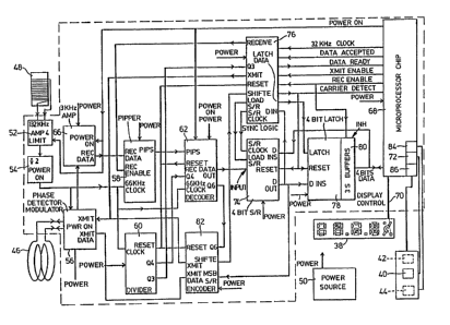
Each module also contains a circuit board which is not
illustrated in Figure 3 but is shown schematically in Figure 4.
The power for each module is provided by a power source
50, which in this embodiment is a lithium battery of 0.2 amp
hour capacity having a potential life for operation with the
circuit of the invention of about 3 - 5 years. In view of the
fact that a typical retail store will contain at least 5,000
modules this is the extent of the life that is preferred by the
industry, since battery replacement of so many modules is a
time-consuming and costly operation. The manner in which the
circuit of the invention is able to obtain such an extended
shelf life with such a battery will be described below.
The base station transmitter transmits a first
reference carrier signal of frequency N, which in this
embodiment is 132 k~z, the frequency being determined by
division down from a crystal controlled oscillator to obtain the
desired stability. Provided the module is powered to receive a
signal, as will be described below, this is received by the
smaller ferrite-cored antenna 48, amplified by amplifier 52 and
divided by an integer n, which in this embodiment is 2, by
divider 54 to produce a demodulating or heterodyning signal of
66 kHz frequency (N/n) that is fed to a circuit 56, to be
described in more detail below, which is operative alternatively
as a bi-phase detector or a modulator. The divider output is
also used as a clock signal and for that purpose is fed to a
pipper 58, a divider 60 and a decoder 62. The transmitter also
transmits an information containing signal, to be described in
- more detail below, consisting of a second carrier at 66 kHz,


- 14 -

l2mls
also derived from the same crystal standard, phase modulated by
a coded digital signal, this second modulated carrier being
received in the module by the larger air-cored antenna 46 and
fed to the circuit 56 configured as a phase detector. The
output of the bi-phase detector is an information-containing
encoded, digital pulse signal with pulses that are
positive-going or negative-going with respect to ground
resulting from demodulation of the second modulated carrier
signal from antenna 46 employing as a demodulating reference the
divided signal from divider 54. This digital output signal is
fed to a narrow band filter and amplifier circuit 66, in which
it is shaped as required and unwanted frequency components ~such
as the 132 kHz harmonic) are removed. In this embodiment a pass
band filter of 3 kHz is employed.
A high Q, ferrite-core coil 48 i8 preferred for the
reference frequency antenna since it is relatively immune from
the effects of ambient noise, which is relatively high in the
particular environment of a food store with extensive lighting,
refrigeration and air conditioning installations, particularly
to the effects of ~spikes~ which might otherwise cause unwanted
frequency and phase changes. On the other hand, a low Q air
cored coil is preferred for the receive/transmit antenna 46,
particularly when it is required to transmit, since more power
can be radiated as compared to a ferrite-cored antenna, and the
receiver bandwidth can be greater to permit higher BAU~ rates to
be used.
Figures 5a - 5e show the sequence of signals beginning
- with that received by the antennae and subsequently that


- 15 -

1~777~

obtained from the phase detector 56. Thus, Figure 5a shows a
typical 132 kHz first carrier signal received by antenna 48, and
Figure 5b shows the resultant divided demodulating reference
signal from divider 54. Figure Sc shows a typical phase
modulated signal obtained from antenna 46 having two phase
transitions at X and Y. The signal at 5d is the output of the
phase detector resulting from detection using the reference
frequency signal 5b, and that at 5e is the resultant signal
after smoothing and filtering, consisting of either positive- or
nesative-going pulses about the zero volt line OV. Since all of
the subse~uent circuits are of binary digital type, the high
pulse value is ~1~, while the low pulse value is ~0~.
The amount of information re~uired to be transmitted to
the module is relatively limited and it is found adequate to
operate with a 32-bit binary opera~ing word, as illustrated by
Figure 6, subdivided into eight 4-bit ~nibbles~ N4 - Nll. The
word is preceded by three password nibbles N1 - N3 and ends with
two sync nibbles N12 and N13, whose function will be described
below. The first data ~ibble N4 of the word is a module
instruction start, while the second nibble N5 is an instruction
modification to the instruction start, the two instructions
combining to instruct the module as to the action that is to be
taken with the data nibbles N6 - N9. The last two nibbles N10
and ~11 are both complement check sum coded for the data
nibbles, this relatively large check sum coding being employed
to ensure accuracy for the data under the difficult conditions
in which the modules operate. The complement is employed to
~ ensure that a positive response is always obtained, so that a

s

~1~ is always detected avoiding the ambiguity caused i no
response were obtained, which might be due to module failure.
Another level of security is provided by encoding the digital
signals at the transmitter and decoding in the module, and
vice-versa when the module is transmitting, using, for example,
bi-phase mark or space coding. Since the system is not in any
way time-critical, a conservative coding system can be employed
despite the fact that it results in half speed transmission.
Such coding of digital data is described, for example, in Pages
384 - 395: 535 - 536 of ~Introduction to Communication Systems~
by F. G. Stremier, published 1982 by Addison Wesley, Redding
Mass, which is incorporated herein by this reference. At the
base station the coding and encoding will be included in the
softWare of the controlling micropr~cessor. The coding system
employed in this embodiment is sUch that upon encoding both ~0~
and ~1~ will produce pulses with transitions at the ends of the
respective bit periods, while a ~1~ will additionally result in
a transition at the middle of a bit period; and vice-versa upon
decoding. A conservative coding of this type has the advantages
that it gives a zero average voltage, which is more certain than
one which gives an average positive or negative voltage that can
vary and perhaps cause loss of data, and that it constitutes a
built in clock making it easier to synchronize the coded and
uncoded bits of the original data. It is found in practice
important that the coding system used is polarity insensitive,
so that initiating conditions of the circuits employed will not
affect the validity of the data.
~ Referring again to Figure 4, the overall control of the
system is maintained by a microprocessor chip 68, which can be a

- 17 -

S
standard chip as employed in a digital watch or clock, such a
chip already including, besides its microprocessor and internal
clock, the registers for the control of the LCD display 38 which
corresponds to the usual LCD watch or clock display; the control
being exercised through connection 70 with the requisite data
stored in the many storage registers provided in the chip. For
example~ the data for item price, which usually must be
displayed continuously, will be stored in the register that is
normally continuously accessed, while the corresponding data for
unit price display is stored in another of the registers which
is accessed to replace the item price information on the display
upon the shopper pressing the visible button 40, the button
assembly being connected to the clock chip through a respective
register 72. The chip also may contain program registers, as
many as three, which can be programmed to cause the chip to
cycle through the display registers in a preset sequence, so
that individual words in those registers can be made to display
in sequence, thus providing a special announcement upon
addressing the particular program register, each program giving
rise to a respective message selected from the words available
in the registers. Such a chip may, for example, have as many as
fourteen display registers, the smallest of which are of 16-bits
capacity with the lead 4 bits available for display
instructions, while the remaining 12 bits are available for
display data; the chip may also contain as many as four
maintenance règisters of smaller capacity, e.g. 8 or 4-bits,
which can be used for other functions such as are described
~ below.


- 18 -

l2mls
Another important function performed by the
microprocessor chip 68 is to provide a much reduced duty cycle
for the radio frequency parts of the module, such as the
amplifiers 52 and 66, which are of relatively high power
consumption. The chip will include a programmable on and off
register and in the chip employed this is of 16-bit capacity
with the first 4 bits used to set the length of turn on time and
the remaining 12 used to set the length of turn off time. Thus,
typically the chip continuously turns on the RF circuits for a
period of 0.5 seconds and, if no first reference carrier signal
is received during that period, it turns them off again for a
much longer period, typically 10 seconds, to give a duty cycle
of 20. As long as the first carrier signal is detected, as
described below, the chip remains turned on until the reference
ceases for the ~R~ ON~ time which in this embodiment i8 O. 5
second duration. Such a cycle will usually increase the battery
life by a factor of about 2 times, since each module is
operative for only a very small fraction of the total time, but
of course the microprocessor chip itself and other parts of the
circuit must remain powered at all times.
The base station will usually remain powered, but
quiescent, until it is instructed to transmit to one or morè of
the modules, whereupon the first reference carrier ls
transmitted for at least 10 1/2 seconds, to ensure that
transmission occurs during the ~on~ portion of all the module
duty cycles; at the end of this transmission all of the modules
will therefore be ~on~. The first carrier is then switched off
for a period of about 50 milliseconds, which is too short for


-- 19 --

S
the modules to switch off, and both the first reference and the
second modu}ated carriers are now transmitted simultaneously.
This permits the first carrier to be used to ~frame~ the
transmitted data and the data received from th~ module, as will
be described below.
Referring again to Figure 4, with the R~ portions of
the module powered by the clock chip signal from ~R~ POWER ON~
and the reference carrier and the modulated carrier received
during that period, the output of the amplifier 66 is fed to
pipper 58 from ~REC DATA~ terminal to ~REC DATA~ terminal, the
cloc'~ signal from the divider 54 being fed to ~66 kHz CLOCK~.
Tne pipper produces an output pulse or pip each time there is a
state change in the received data and these are fed from its
~PIPS~ terminal to the ~PIPS~ terminal of the decoder 62 which
decodes the bi-phase coded data back to normal binary code
data. ThusJ the decoder, which also receive3 the 66 kHz clock
signal, determines whether a pip occurs in the middle of a time
period and, if so, generates a ~1~ and, if not, generates a
~0~. The decoded binary signal is fed from terminal ~DEC DATA
OUT~ to terminal ~INPUT~ of a 4-bit shift register 74 in which
the signal shifts while the data in the register is fed from
terminal ~D OUT~ to terminal D IN~ of sync logic circuit 76.
When synchronism is detected by sync logic circuit 76 between
the first password nibbles Nl - N3, and after a one nibble
delay, a ~LATC~ DATA~ signal is sent from that terminal of
circuit 76 to the ~LATCH~ terminal of a 4-bit latch 78, and the
subsequent data nibbles N4 - Nll are subsequently latched into
the latch from terminal ~D OUT~ to terminal ~D IN~, and fed


- 20 -


through tristate bufers 80 to the ~4-BITS DATA~ terminal of the
microprocessor chip for utilization therein. Tristate buffers
are required since the data moves in both directions to and from
the microprocessor. The password Nl - N3 will be the same for
all modules and is employed to ensure that the module does not
attempt to respond to spurious data; three nibbles are employed
for added security; typically, the word will be a unique three
digit number, the first of which will usually be zero. The
first transmission or transmissions supplied to the chip 68 have
in the instruction and data nibbles N4 - Nll an identifying
instruction or instructions for the module to be addressed; upon
the chip 68 detecting that it is being addressed, it is enabled
to receive further data and write it into its registers, while
if it does not detect an identifier, it remains quiescent and
ignores the further data received from the buffers.
As will become evident, it is essential for correct
operation that the reference carrier is present; it is detected
by divider 60 which trans~its a one-sixteenth divided clock
signal (4125 Hz) from terminal Q3 to the corresponding
terminal Q3 of the sync logic 76; effectively the sync logic
circuit counts the number of cycles received in a time period
set by this clock signal and, if sufficient are counted for this
to be the required carrier, it sends a ~carrier detect~ signal
to the respective microprocessor chip terminal, whereupon the
clock chip returns a ~receive enable~ signal to the sync logic.
The carrier detect signal is also used as the reset signal for
the shift register 74 and the latch 78. The sync logic also,
- upon detection of the required password Nl - N3 flags the chip


- 21 -

1;~77~S

68 through the ~DATA R~DY~ connection every four bits
synchronous with latching the data into the latch, so that it is
ready to receive the data to be used. Upon conclusion of the
receipt of each four bits, the ~data ready~ signal is cleared by
~he microprocessor chip by pulsing the ~DATA AC OE PTED~
connection.
Upon the reference carrier ceasing, the carrier detect
signal to chip 68 also ceases and a time out time period starts
to operate that will usually be of the same length as the turn
on time and produced by the same register, the RF circuits being
switched off after this time until a new time out period of 10
seconds elapses. This means that instructions to the module
must be transmitted at a rate faster than this off time period.
A system as already described with individual battery
operated modules, each of which can be individually addressed by
a broadcast transmitter, so that no hard wiring is required, is
already of great value in the type of installation to which it
is directed. Some way usually is needed to confirm that data
has been safely received, and systems for this will be described
below. However, the value of the system is even greater by
providing that the modules can transmit appropriate information
back to the base station and the store computer. For example,
it is then possible for re-stocking personnel to walk along the
aisle and immediately upon visual inspection of an item transmit
back the identity of the item, its current shelf location and
the quantity required for re-stocking. All of this is to be
accomplished, if possible, without decreasing the battery life
more than is absolutely necessary, in order to achieve the


- 22 -

127771S
desired target of 3 - 5 years life or longer. The manner in
which this is accomplished in this embodiment will be described
after further description o the protocol employed to transmit
data to the module.
As has been indicated above, the operation of a radio
frequency broadcast system of the invention involves two
different difficult problems, namely the extremely noisy
environment in which the inherently low power system must
operate, and the need for extreme battery life which implies
extremely low power consumption. The power of the base station
can of course be made as high as is necessary with relatively
low additional cost. A phase modulated system is selected
because of its inherent high noise tolerance, and digital coding
of the transmitted data is employed again because of the low
power digital circuit elements than can be employed to
manipulate such data. Encoding of the transmitted digital
signals in both directions provides yet another level of
security for the subsequent accurate detection of the data. The
conventional procedure in demodulating phase modulated signals
2~ is to employ a phase locked loop in the detector, but in the
very noisy environments encountered there is the danger that the
loop would lock onto adjacent interference instead of the
signal, or take so long to lock onto the signal among the
ambient noise that data transmission becomes impossibly slow,
even though speedy transmission is not usually required. A
phase locked loop therefore would need to be kept in constant
operation and could not duty cycle as described above, and would
in addition require an accurately controlled oscillator and thus


- 23 -

1*~71~

involves a considerable power consumption in each module. For
example, a circuit employing such a loop that was prepared
required an operating current of about 50 microamps, which is to
be compared with the average consumption of about 5 microamps
achieved with the module described, in which the chip 68
required an operating current in the range 3 - 5 microamps. The
need for such a loop is avoided by the apparatus of the
invention employing a reference frequency generated by the base
station and divided in the module to provide the demodulating
reference for the lower frequency data-carrying signal.
Another aspect of the invention leading to lower power
consumption is the choice of an operating frequency in the range
10 - 500 k~z. The power consumption of digital devices, such as
the C~OS type that usually are employed because of their low
cost and power consumption, i8 directly proportional to the
number of switching transitions required for operation, and the
low speeds selected are completely adequate for the re}atively
low speed data transmission that is required. Broadcast signals
in this range of frequencies inherently are of short range, so
that with the employment of a segmented antenna power
consumption is reduced, since only a specific group of modules
can be addressed, and the unwanted modules do not receive data
only to ignore it when it is not addressed to them. The low
frequency also facilitates the electromagnetic coupling to the
metal shelf units as described above, which also limits the
effective range of each antenna segment. With much higher
frequencies, there is the greater possibility of phase shift
-with the different distances of the modules from the store


- 24 -

lm71S
antenna, although this can be compensated with the system of the
invention, as described below. The initial instruction from the
base station will be preceded by control signals to the required
switches 27 to turn on the respective antenna segments, the
switches all being reset to open upon conclusion of the
transmission. There will, however, be applications of the
invention in which such lengthy battery life and restricted
range are not required, and in such cases the freauency employed
can be very much higher, for example up to 50 M~2.
1~ Referring now to Figures 7a through 7e, a further
aspect of the invention to combat the noisy environment is that
the data is transmitted from the base station in the form of
discrete words that are framed by a reference envelope of the
reference frequency transmission. Moreover, if the module is
instructed to transmit back to the base station, then each data
word transmitted by the module is also framed by the reference
envelope containing that instruction; in addition, the module
data word is located precisely within the reference envelope, so
that the base station will have correspondingly precise
information as to the start time when the module transmits the
word and can therefore more easily detect its leading edge, even
in considerable noise, and accurately read the corresponding
data. Figure 7a illustrates the reference envelope of the 132
kHz reference signal that is generated by the base station
transmitter in response to instructions from the controlling
microprocessor, the duration or length of the envelope being
fixed as described below. Receipt of the envelope by the module
- generates the carrier detect signal (Figure 7b) from the sync


- 25 -

lm 7~S
logic 76 with a slight propagation delay (of the order of 2
milliseconds in this embodiment) between the respective leading
and tra~iling edges through the system, and this is followed by
the rec:eive enable signal from chip 76, again with a small
system delay. The chip now receives the base station
transmitted word (Figure 7c~ and it will be seen that, owing to
the system delays, part of the first nibble Nl may not be
received: it is for this reason that a very generous three
nibble password instruction is employed, and the first nibble
will usually be zero, so that its loss is immaterial. The
receive enable signal ceases at or close to the end of the word
and may occur during the word at sometime during N12; the
receive signal is synchronized by the sync logic to terminate at
the end of N12. A very generous two nibble complement chéck sum
~10 - Nll is provided for increased securit~.
The base transmitted instruction N4 - Nll may be such
that no specific response is required from the module; for
example, it may simply provide a new item price and unit price
to be inserted in the respective register. It will usually be
preferred that some response is provided, even if only an
acknowledgement from the microprocessor chip that data has been
received and entered, and the system of the invention permits
ready confirmation that the data from the control computer has
been received. If such an acknowledgement is not received by
the base station, then it can be programmed to repeat the word
for a specific number of times, perhaps with the same number
repeated after one or more intervals; if after a specified
- number of such attempts still no acknowledgement is received,


- 26 -

~Z77715
then the computer will be advised of the nil response and will
flag l:hat the unresponsive module requires examination by
service personnel. The reference frames are also transmitted
spaced a precisely fixed period apart, the period between being
sufficient to ensure that the somewhat slow acting module can
take the necessary action; in this embodiment the preferred
period is 100 milliseconds. A typical instruction requiring a
response that is more than an acknowledgement is to read out the
contents of a maintenance register that have been addressed by a
re-stocking clerk with information as to the re-stocking
quantity required. The receive enable signal goes low as
described above and sync logic 76 synchronizes the receive
enable signal to the trailing edge of the nibble N12 and
computes a precise period Tl beginning at the trailing edge of
last data nibble Nll for transmis~ion to begin of the module
transmit word nl - n6. This is done by the divider 60, decoder
62, encoder 82 and counters in the sync logic 76 continuing to
run, with the sync logic counting four bit periods at the lower
transmission BAUD rate until the transmit enable line goes high,
whereupon at the leading edge of the next four bit period
transmission begins. A period T2 also timed from the trailing
edge of the nibble Nll is made shorter than Tl, as described
below, to ensure that the module is enabled for transmission
before it is required to transmit the module package signal.
The phase detector/modulator 56, operative as a modulator
transmits encoded zeros resulting from data left in the shift
registers, which must be zeros since the pipper is not
operative, until it receives valid data for transmission which


27 -


i;~77715

begins at the leading edge of the said next four bit period.
The transmit enable signal (Figure 7e) embraces the period
required for the module transmit word to be transmitted from the
module. As described above, the base station transmitter has of
course the information as to the


27a -

127~715
duration of nibbles Nl - Nll of the transmitted instruction and
by adding the known period Tl has information as to the
precise time of receipt of the leading edge of module transmit
nibble nl. The transmit enable signal is made as short as
S possible to conserve power.
The length of period Tl is made such that the
microprocessor chip is able to carry out any computation that is
required before providing the corresponding transmit
information. In this embodiment the module transmit word
}0 consists of 24 bits, consisting of a 16-bit, four nibble
instruction nl - n4, and an 8-bit, two nibble complement check
sum nS and n6. Again, in view of the noisy environment and the
low power available for module transmission, the BAUD rate for
the module transmission is made much lower than for the much
higher powered base station transmission so as to increase the
effective signal-to-noise ratio, and in this embodiment, while
the base station transmit rate is 1375 ~AUD, the module transmit
rate is 258 BAUD.
The transmit enable signal is sent from ~XMIT~ terminal
of the sync logic to the corresponding terminals of the encoder
82 and the phase detector and modulator 56, the latter being
switched by the signal to function as a modulator of the 66 k~z
signal it has been receiving from divider 54. The data to be
transmitted goes from the ~4-BI~S DATA~ terminal of chip 68
directly to the shift register 74 at ~D INS~ where it is counted
by the sync logic 76; each time a 4-bit nibble is counted, the
logic 76 advises chip 68 via connection ~DATA READY~ so as to
- receive the next nibble and instructs the shift register via

~7is
~LOAD S/R~ tsend/receive) and ~S/R CLOCK~ to transmit the nibble
one bit at a time (the most significant bit) to the encoder,
which e!ncodes into bi-phase code. The coded signal goes from
~IT DATA~ terminal to the corresponding termina} of the
circuit: 56 which modulates it on to a 66 kHz carrier and sends
the resultant phase modulated signal to the antenna 46 for
broadcast transmission to the base station.
Each of the two ~concealed~ buttons 42 and 44 is
connected to a respective register 84 and 86 of the chip 68 and
can be employed for different functions as those registers are
instructed by the store computer. For example, as described
above, one of the chip maintenance registers can be employed to
record the re-stocking required for the item to which it
relates. When this is required, the two buttons can be
designated by their registers respective}y to increase and
decrease the value recorded in this register, so that the
required value is available when subsequently the chip is
instructed by the store computer to advise it of the stored
value. When assigned the respective function the buttons can be
used to increment or decrement the facings register, or can by
means of an assigned code of button pushes instruct the
computer, for example, that a particular item is ~SOLD OVT~ on
the shelves.
One of the practical difficulties encountered with a
system functioning as a unitary network is that there are many
different individuals within a store that have to control
different parts of the store at the same time. For example, in
-a typical supermarket store, there may be as many as 10 - lS


- 29 -

lm~iS
employees responsible for different ais}es. Employee one may
want to put his/her ais}e in a mode such that the modules
display~ the backroom inventory. A second employee may want to
be reordering. Employee three may want to display the number of
facings of the items to check that they are in accordance with a
revised store plan (planogram), etc. One solution would be that
all the employees could refer to a computer supervisor, or could
be taught how to use the computer; but these are not very
practical.
In accordance with the invention, to meet this
requirement there are placed in the store at different locations
for easy access by the personnel involved a number of modules
that are not associated with a specific product, but instead can
be used by the personnel to transmit information to the store
computer as required. The most 5atisfactory location is on a
shelf in the appropriate location; since it can be accessed by
the public, it is desirable that a specific security code of
button pushes of the visible button 40 be required before the
module can access the computer, or before the concealed buttons
are enabled. ~hese independent modules can be polled by the
computer at regular intervals, for example every 30 seconds, to
determine if the security code has been entered, and if so what
action or information the operator requires. For example, by
inserting a predetermined code of button pushes with the visible
and/or the concealed buttons, the computer may be instructed to
place the specific aisle in the required mode (e.g re-ordering,
facings, available stock, etc.), so that the operator can now
move along the aisle operating each of the fixed modules to


- 30 -


transmit the corresponding information to the base station
computer. The preferred mode of such an operation is for the
operator to instruct the store computer to enable all of the
associated modules to receive the required information by means
of a button code inserted via any of the buttons, or any
combination thereof. The operator then moves along the aisle,
or shelf, operating each module, again by a predetermined button
push protocol, to insert the required information. When this is
completed the mode module can then be operated to instruct the
computer that the modules are ready and available for the
information to be retrieved.
Anothèr problem that is addressed and mitigated by the
system results from the manufacturing constraints in producing
apparatus that is sufficiently cost effective for industrial
use, particularly a low margin industry such as food retailing.
The antenna coils must be tuned as closely as possible to the
operative frequency, particularly the high Q coil 48, but this
can be expensive, requiring sophisticated winding machines
and/or choice of low tolerance (and consequently expensive)
components, or the use of tunable cores and components. The
coil 48 can therefore have a resonant frequency which is as much
as + 1 kHz from the required value. Again, the assembly of the
circuit board, particularly the connection of the antennas, can
result in changes in the phase response of the assembled module,
which will differ from module to module. The location of the
module relative to the store antenna, its position on the metal
shelving, and whether or not the associated items are in metal
or non-metal containers can also affect its response. This


lZ77715

probleM is mitigated by the system illustrated schematically by
Figure 8, wherein each module 14 is first mounted at its
operatlve location, before operative data is transmitted to it
and, then there is transmitted from base station 24 a standard
S signal of phase designated as of zero phase, which signal
instructs the module to respond with a return signal; the
voltage of the return signal received at the base station via
its detector 24a is measured and recorded also at a phase
designated as of zero phase. This transmission is repeated
while the phase of the detector at the base station is cycled in
discrete equal increments through 180 by phase changer 24b it
has been found in practice that it is quite adequate to change
the phase in this manner through eight equal steps of 22 1/2
each. The eight values that result are plotted as the bottom
line of the table in Figure 9. The phase o~ the transmitted
signal is then changed by the same size step (i.e. 22 1/2) via
phase changer 24c operative with transmitter modulator 24d, the
phase of the detector again cycled in eight steps through 180
and the results plotted. This procedure is repeated until the
phase of the transmitted standard signal has also been cycled in
eight steps through 180. In practice this cycling and
recording will be under the control of 3 program in the store
computer. A typical plot of the 64 results thus obtained is
shown in Figure 9, wherein a star shows a good combination, a
cross shows a combination in which some data error occurred and
should therefore be avoided, and a dot shows an unusable
combination. One of the usable combinations, preferably one
among a number of adjacent high values, is then selected and


- 32 -

i277'71~

programmed into the computer to be used with that module during
any interaction with it. It will be seen therefore that
considerable tolerance is available in the system as operated to
compensate for quite wide tolerance in this electrical
cnaracteristic of the module circuit.
Referring now to Figure 10, the pipper circuit 58 in
this embodiment is operatively a 2-bit shift register,
consisting of two flip-flops 88 and 90, which are fed from its
receive data terminal and 66 kHz clock terminal, the flip-flops
requiring both clock and clock invert inputs for operation. The
flip-flops are enabled as described above upon receipt of a
signal on the receive enable terminal, their outputs being fed
to an exclusive OR gate 92 which produces the output that is fed
to the decoder. Thus, if the received data has a change of
state from 1 to 0, or 0 to 1, then the transition is shifted in
the shift register formed by the flip-flops, and there will then
be a difference between the states of 88 and 90 as fed to the
gate 92. If such a difference occurs, then an output pulse is
generated by the gate and fed out at the ~PIPS~ terminal.
Referring now to Figure 11, in the decoder circuit 62
the pips received from the pipper circuit 58 on the ~PIPS~
terminal can be of two categories, namely reset pips which are
those produced at the ends of each transition and the data pips,
which are those produced between bit end transitions, as
detected by their time of occurrence, to indicate that the data
is a ~1~ or ~higha. These pips are fed to NAND gates 94 and 96,
the latter resetting the decoder data out terminal via NAND gate
98, inverter 100 and flip-flop 102, provided gate 98 is enabled


- 33 -

1277715

by an RF ON signal. The other input of gate 94 is fed from
flip-flop 104 which is clocked by the 66 kHz signal from divider
54 received on the respective terminal. This flip-flop receives
its input at terminal D from two series connected flip-flops 106
and 108 that are clocked by the Q4 signal from divider 60 at
one-sixteenth the clock rate (i.e. 4125 Hz with pulse length 242
microseconds); these count the input pulses and the state of
flip-flop 108 output determines whether the pip is a reset or
data pip; the output of flip-flop 108 is fed through flip-flop
104, and it is the output of the latter that is fed to gate 94
and NAND gate 110, the purpose of this flip-flop being to ensure
that the pulses are of specific length, in this embodiment 15
microseconds. The output of gate 94 feeds NAND gate 112, which
also receives the RF ON signal, and which generates the reset
pulses fed to the RESET terminal, and also the flip-flops 106
and 108. It will be seen that the circuit is continuously reset
to 0, whenever ~RF ON~ is not on, which also ensures that noise
cannot operate the circuit. The flip-flops 106 and 108 count
the time from the previous reset pip and the two NAND gates 96
and 110 gate a pip, that from its timing is a data pip, to the
data output flip-flop 102. The output Q6 of flip-flop 108 is
employed in the encoder 82 and the decoder therefore runs freely
whether or not it is being employed to decode. Inverters are
required throughout this and the other circuits to provide the
necessary signal direction, as is apparent to those skilled in
the art, and need not be specifically identified. Also, the
signal required for correct operation may be the signal itself,
-or its complement ( _B ), or both, as is apparent to those


- 34 -

1i~7~715
skilled in this ar~, and specific identification of this
function is not required.
Referring now to the encoder circuit of Figure 12, the
two fli.p-flops 114 and 116 again comprise a two stage counter
that is fed from Q6 and Q6_B of the decoder, which is one
quarter of the input frequency to the encoder (i.e. 1031 Hz)
because of the lower ~3AUD rate at which the module transmit data
is transmitted. Output flip-flop 118 is clocked from the output
of flip-flop 114 twice per transmit bit period, and the output
of flip-flop 116 fed through NAND gates 120, 122 and 124, and
exclusive OR gate 126, ensures that flip-flop 108 will always
toggle on the end of a bit period: it is toggled twice per bit
period and, in the middle of the bit period when flip-flop 116
is not set, the state of the most significant bit incoming on
terminal MSB_SR rom shift register 74 determines whether or not
there is an additional mid-period toggle. The output of
flip-flop 116 also feeds from the encoder at terminal "SHIFT E~
to the sync logic 76 and thence via ~ LOAD S/R" and ~S/R CL~
to lock the shift register while each bit is clocked and encoded.
Referring now to the sync logic circuit of Figure 13,
the 32 kHz clock signal that is available from chip 68 is fed to
a 5 flip-flop divid~r chain 128 - 136, the resultant square wave
1 k~z signal from final flip-flop 136 clocking a sixth flip-flop
138. The output of flip-flop 136 also feeds through a three
inverter chain 140 - 144 providing a single inversion, the
middle one of which is a slow inverter to also provide a time
delay into NAND gate 146 which produces pulses corresponding to
each pulse leading rising edge. A following NAND gate 148 is


-- 35 --

1~

enabled by the ~RF ON~ signal and feeds these pulses as resets
to a pulse counter chain of flip-flops 150 - 156, which further
counts down the Q3 signal that was originally the 132 kHz
first rèference signal to a frequency (.6875 kHz) at which it
can be compared with the 1 kHz signal derived from the chip
clock. The flip-flop 138 is therefore the carrier detector and
outputs on the respective terminal. At the same time it
releases an RS flip-flop constituted by NAND gates 158 and 160,
which is used to detect whether or not the password nibbles Nl -
N3 are valid ~in this embodiment 005) so that the subse~uentdata nibbles will be accepted. In hexadecimal 5 is the number
0101 and when this correspondence is detected by the combination
of MOR gate 162 and NAND gate 164 fed in at terminals D(O),
D(l), D~2) and D(3) the RS flip-flop is set and in this state
releases the three 1ip-10ps 166, 168 and 170 to run. The two
flip-flops 166 and 168 count the four bits of each nibble and
feed flip-flop 170 through ~IOR gate 171, the flip-flop providing
a l-bit delay for timing purposes, its output being the latch
signal exiting on the ~ LATCH~ terminal so as to latch the nibble
into the shift register. The latch signal also sets flip-flop
172 which gives the ~DATA READY~ signal to the chip 68
indicating that data is in the latch 78 ready for output from
the latch; this flip-flop is reset by the chip by an input
signal on ~DATA ACCEPTED~ after the data has been read by it.
The latch signal from 170 also clocks the flip-flop 174 which,
together with the NAND gates 176 - 180, comprise a circuit to
synchronize the receive enable with the latch and ensure that it
- ceases at the required point in the base station word, namely at


- 36 -

the end of nibble N12, the additional nibble N13 being provided
to give redundancy. The transmit enable signal from the chip 68
is fed to a NOR gate 182 with this synchronize signal and
resulls in the ~LOAD S/R" signal for the shift register in order
to shift each nibble from the register to the encoder. The
~SHIFT E~ signal from the encoder feeds into the sync logic and
through NOR gate 184 to the flip-flop 170. The timing of the
period Tl (Figure 7c) from the trailing edge of the data
nibble Nll has been described above. A second shorter period
T2 (Figure 7e) between the trailing edge of Nll and the
beginning of transmit enable is the responsibility of the
microprocessor chip; this is the period during which the
microprocessor carries out its calculations and is not known as
precisely as period Tl and in this embodiment is approximately
44 milliseconds long and about 2 milliseconds shorter than Tl.
Referring now to Figure 14, the phase detector and
modulator 56 includes a timing capacitor 186 connected across
the 66 kHz coil 46 between two junctions of a bridge formed by
four transmission gates 188 - 194, the other two junctions being
connected between ground and the ~POWER ON~ terminal via
transmission gate 195. The gates are connected so that either
the pair 190/192 or the pair 188/194 are conducting, so that
depending on the pair that is conducting the corresponding end
of the coil is grounded and the phase is reversed by 180. The
66 kHz signal is fed to an exclusive OR gate 196 that also
receives the XMIT DATA signal from the encoder 82 that in the
receive mode is held low, whereupon the output is the same as
the input, namely the 66 kHz signal multiplied by plus or minus


- 37 ~


s

one, which is applied to the bridge to demodulate the phase
modulated 66 kHz signal received by the antenna 46. The circuit
also includes two other transmission gates 198 and 200 and all
three ~ates are controlled from the X~1IT ENABLE terminal. Thus,
when receiving, this is also held low whereupon devices 196 and
200 are disabled and device 198 is enabled, so that the
demodulated signal at the junction 202 of the bridge is fed to
the amplifier 66.
In the transmitting mode the X~IT E~lABLE signal now is
high and gates 196 and 200 are enabled; gate 198 is disabled so
that amplifier 66 is connected to ground through gate 200 and no
signal can be fed thereto. The word to be transmitted is fed in
on XMIT DATA terminal, when the data signal is low the output of
the exclusive OR gate 196 is the same as the input, again the 66
k~Iz clock signal; when the data signal is high the output is
inverted, so the phase of the signal at 202 is modulated in
accordance with the data and this is applied across the coil 46
which resonates and transmits it to the respective antenna
segment.
In the embodiment described above, the power source 50
for the module comprises a lithium battery of a capacity able to
provide the average current drawn by the module circuits of
about 5 microamps for about 3 - 5 years. An alternative source
is illustrated by Figures 1 and 15, consisting of a rectifier
bridge 204 in the module connected directly to the antenna 48
and supplying the energy thus received to charge a high value
capacitor 206 whose maximum charge voltage is determined by a
- zener diode 208. It is now possible to obtain small relatively


-- 38 --

1~77 7~5
low cost capacitors of capacity as high as 1 Farad, and such a
capacitor will provide a current of 5 microamps for a period of
as long as a week, so that there is sufficient power to maintain
the module R~s even in the event of a power failure.
Alternatively, the capacitor could be replaced by a battery of
rechargeable type. The power to operate the charging circuit
could be obtained from the base station transmitter 24, but
instead a dedicated transmitter 210 may be provided for this
purpose that is operated by the store computer during periods
that the modules are not re~uired.
Although the combination of an air-cored and a
ferrite-cored module antenna has been described, it will be
apparent that both antennae can be ferrite-cored; it will not
usually be preferred to employ an air-cored antenna also for the
reference signal for the reasons described above, and it becomes
difficult to arrange two large air-cored antennae in a compact
module casing because of the need for orthogonal disposition.
the two ferrite-cored antennae can be located in an ~L~ or ~T~
formation relative to each other.
Although in the systems described phase modulation has
been employed, it is also possible to employ amplitude
modulation of the second carrier.


- 39 -

Representative Drawing
A single figure which represents the drawing illustrating the invention.
Administrative Status

For a clearer understanding of the status of the application/patent presented on this page, the site Disclaimer , as well as the definitions for Patent , Administrative Status , Maintenance Fee  and Payment History  should be consulted.

Administrative Status

Title Date
Forecasted Issue Date 1990-12-11
(22) Filed 1987-09-18
(45) Issued 1990-12-11
Deemed Expired 2002-12-11

Abandonment History

There is no abandonment history.

Payment History

Fee Type Anniversary Year Due Date Amount Paid Paid Date
Application Fee $0.00 1987-09-18
Registration of a document - section 124 $0.00 1989-06-27
Maintenance Fee - Patent - Old Act 2 1992-12-11 $50.00 1992-12-10
Maintenance Fee - Patent - Old Act 3 1993-12-13 $50.00 1993-12-02
Maintenance Fee - Patent - Old Act 4 1994-12-12 $50.00 1994-12-09
Maintenance Fee - Patent - Old Act 5 1995-12-11 $75.00 1995-11-20
Maintenance Fee - Patent - Old Act 6 1996-12-11 $75.00 1996-11-29
Maintenance Fee - Patent - Old Act 7 1997-12-11 $150.00 1997-11-14
Maintenance Fee - Patent - Old Act 8 1998-12-11 $150.00 1998-11-19
Maintenance Fee - Patent - Old Act 9 1999-12-13 $150.00 1999-11-10
Maintenance Fee - Patent - Old Act 10 2000-12-11 $200.00 2000-11-20
Owners on Record

Note: Records showing the ownership history in alphabetical order.

Current Owners on Record
STEVENS, JOHN KING
TELEPANEL INC.
Past Owners on Record
WATERHOUSE, PAUL INGRAM
Past Owners that do not appear in the "Owners on Record" listing will appear in other documentation within the application.
Documents

To view selected files, please enter reCAPTCHA code :


To view images, click a link in the Document Description column. To download the documents, select one or more checkboxes in the first column and then click the "Download Selected in PDF format (Zip Archive)" or the "Download Selected as Single PDF" button.

List of published and non-published patent-specific documents on the CPD .

If you have any difficulty accessing content, you can call the Client Service Centre at 1-866-997-1936 or send them an e-mail at CIPO Client Service Centre.


Document
Description 
Date
(yyyy-mm-dd) 
Number of pages   Size of Image (KB) 
Drawings 1993-10-14 11 258
Claims 1993-10-14 47 1,609
Abstract 1993-10-14 1 51
Cover Page 1993-10-14 1 12
Representative Drawing 2001-09-25 1 25
Description 1993-10-14 40 1,638
Fees 2000-11-20 1 33
Fees 1999-11-10 1 40
Fees 1998-11-19 1 52
Fees 1996-11-29 1 47
Fees 1997-11-14 1 40
Fees 1995-11-20 2 112
Fees 1995-10-26 1 39
Fees 1994-12-09 1 43
Fees 1993-12-02 1 33
Fees 1992-12-10 1 31