Note: Descriptions are shown in the official language in which they were submitted.
~ ~7772~ S03003
BACKGROUND OF THE INVENTION
Field of the Invention-
~ his invention relates generally to a logiccircuit of the differential amplifier kind for performing
logic operations on binary input signals and, more
particularly, to a logic circuit particularly adapted for
integrated circuit fabrication in which a separate reference
voltage generating element is not required for the
differential amplifier circuit.
Description of the Prior Art:
The particular requirements of integrated circuit
fabrication have forced changes in the design of various
logic circuits from their original, discrete-component
designs. For example, the constraints on such logic circuit
designs placed by the integrated circuit fabrication
techniques have resulted in the use of differential
amplifiers and constant current sources as a fundamental
building block for such logic circuits, and this kind of
logic circuitry is typically referréd to as emitter coupled
logic (ECL). Representative of this technology is V.S.
Patent No. 3,259,761. Central to such ECL differential
amplifier logic, is the requirement for a reference voltage
generator to provide the necessary reference voltage against
which the input signals are compared. Further, in order to
provide high-speed logic circuits, the current that must
flow through each logic circuit is necessarily large
relative to the quiescent state, and accordingly the number
of reference voltage generators must correspond roughly to
the scale vf the l~gic circuit, so that they are capable of
,, .
--2--
~27~ S03003
I
absorbing the transient currents produced upon switching the
various transistors making up the ECL logic circuit. Due to
such reference voltage requirements, it is the commonly
known techni~ue to employ three transistors to realize a
two-input OR gate in the ECL differential amplifier
configuration.
Accordingly, the presently known conventional
logic circuits have an inherent disadvantage in that they
require a relatively large number of circuit elements.
Moreover, because of the requirement to employ the reference
voltage an additional wiring pattern for each logic circuit
i8 required and a further disadvantage is present because
the ratio of the area of the wiring pattern on the substrate
is large, and this leads to corresponding increa~es in chip
~ize.
OBJECTS AND SUMMARY OF THE INVENTION
.. ..
Accordingly, it is an object of the present
invention to provide a logic circuit for fabrication as an
integrated circuit that can eliminate the above-noted
disadvantages inherent in the prior art.
Another object of this invention is to provide a
logic circuit that requires no reference voltages or
reference voltage generators, whereby the number of circuit
elements such as transistors and resistors is reduced, with
a corresponding reduction in power consumption and a
reduction in operating time.
In accordance with an aspect of the pre~ent
invention, the differential amplifier is constructed whereby
the ~alue of the constant current source therefor is made
--3--
127772~
S03003
relatively small, yet an operating speed substantially the
same as that of conventional emitter coupled logic is
obtained. Thus, not only is the num~er of circuit elements
reduced but the power consumption required thereby is also
reduced.
By eliminating the requirement for the reference
voltages and the corresponding reference voltage generators
for each of the various gate circuits forming the particular
logic circuit, the wiring pattern used to supply such
reference voltage is eliminated as well and the integrated
circuit chip size can be reduced accordingly.
The present invention, thus, provides a technique
for forming a logic circuit in which the emitters of first
and second transistors are connected to a constant current
source and in which a first lnput terminal receiving the
fir6t binary input ~ignal i~ connected to the base of the
first transistor and a second input terminal receives the
second binary input signal and is connected to the base of
the second transistor, the output terminal of the logic
circuit i6 then obtained from one or the other of the
collectors of the first and second transistors. The circuit
is constructed so that the amplitude or voltage difference
between a low level and a high level of the first binary
input and of the second binary input are selected to be
equall and one of the first or second binary inputs is
fihifted in level relative to the other by an amount e~ual to
1/2 of such selected amplitude, the output circuit then
provides similarly level shift signals, all of which have
the same absoulte amplitude difference.
--4--
~7772~ S03003
The above and other objects, features, and
advantages of the present invention will become apparent
from the following detailed description of illustrative
embodimlents thereof to be read in conjunction with the
accompanying drawings, in which like reference numerals
refer to like elements.
BRIEF DESCRIPTION OF THE DRAWINGS
Fig. 1 is a schematic circuit diagram of an
emitter coupled logic circuit known in the prior art;
Fig. 2 is a representation of the relative voltage
levels used in the circuit of Fig. l;
Fig. 3 is a representation of a two-input,
two-output OR gate known in the prior art;
Fig, 4 is a representation of a R-S flip flop
known in the prior art;
Fig. 5 is a schematic diagram of an embodiment of
a logic circuit according to the present invention;
Fig. 6 is a representation of relative voltage
levels employed in the circuit of Fig. 5;
Fig. 7 is a representation of a two-input logic
circuit obtainable from the embodiment of Fig. 5;
Fig. 8 i~ a schematic diagram of another
embodiment of a logic circuit according to the present
invention;
Fig. 9 is a schematic diagram of a further
embodiment of a logic circuit according to the ~resent
invention;
~ 127772~'2 S03003
Fig. 10 is a schematic diagram of still a further
embodiment of a logic circuit according to the present
invention;
Fig. 11 is a representation of relative voltage
levels employed in the circuit of Fig. 10;
Fig. 12 is a representation of logic circuit
elements that are obtainable by the embodiment of Fig. 10;
Fig. 13 is a representation of an R-S flip flop
that is obtainable by an embodiment of the present
invention;
Fig. 14 is a representation of logic circuit
elements that may be functionally obtained by an emb~diment
of the present invention;
Fig. 15 is a schematic diagram of an R-S f}ip flop
according to an embodiment of the present invention;
Fig. 16 is a timing chart showing voltage
waveform useful in explaining the operation of the R-S flip
flop of Fig. 15;
Fig. 17 is a representation of an R-S flip flop
that is obtainable by an embodiment of the present
invention;
Fig. 18 is another representation of the logic
circuit elements f~rming an R-S flip flop as shown in Fig.
17;
Fig. 19 is a circuit diagram of an R-S flip flop
as shown in Fig. 18 according to another embodiment of the
present invention;
Fig. 20 is a waveform diagram showing relative
voltage levels present in the R-S flip flop of Fig. 19;
1~72.~ S03003
Fig. 21 is a representation of logic circuit
elements forming an R-S flip flop that may be functionally
obtained by another embodiment of the present invention;
Fig. 22 is a representation of logic circuit
elements forming an R-S flip flop that is functionally
obtainable according to an embodiment of the present
invention;
Fig. 23 is a circuit diagram of an R-S flip flop
according to another embodiment of the present invention;
Fig. 24 is a waveform diagram showing relative
voltage levels of the R-S flip flop of Fig. 23;
Fig. 25 is a circuit diagram of an R-S flip flop
according to another embodiment of the present invention;
and
Fig. 26 i8 a representation of a logic circuit
functionally obtainable according to the embodiment of Fig.
25.
DETAILED DESCRIPTION OF PREFERRED EMBODIMENTS
As known in the prior art, emitter coupled logic
circuits typically fabricated in an integrated circuit
configuration require various reference voltage levels in
order to make the logical comparisons. Fig. 1 is a circuit
diagram of such prior art emitter coupled logic circuit, in
which three transistors 10, 12, and 14 have respective
emitters connected in common to a common or return line
having terminal 15 through a resistor 16 that functions as a
constant current source. One input signal terminal 18 is
connected to the base lead connection of first transistor 10
and the other input signal terminal 20 is connected to the
127772~ S03003
base lead of second transistor 12. The required reference
voltage is then connected to the base lead of third
transistor 14. The respective collector circuits of
transistors 10 and 12 are connected together through
resistor 24 to voltage source terminal 26, and such
collectors also provide one output signal of the logic
circuit at terminal 28 through an emitter-follower
configuration transistor 30. The emitter-follower
configuration of transistor 30 being accomplished by
resistor 32 connected between the emitter lead of transistor
30 and the common or return line terminal 15. In reference
voltage transistor 14, the collector circuit is connected
through resistor 34 to the power source terminal 26 and is
similarly connected to the base lead of transistor 36 that
is al80 connected in emitter-follower conf~guration. The
other output at terminal 38 is provided by emitter-follower
transi~tor 36 acrocs emitter resistor 40 connecting the
emitter circuit of transistor 36 to return or common line
terminal 15.
In the circuit of Fig. 1 and assuming that the
inputs A and B at terminals 18 and 20, respectively, would
be at substantially the same levels typically produced by
such circuit at output terminals 28 and 38, the logic
functions of this circuit are shown in Fig. 3, that is, this
logic circuit functions as an OR gate and a NOR gate.
The relative voltage levels of the high and low
signal levels of the inputs at 18 ~nd 20 in relation to the
reference voltage Vr applied to terminal 22 are shown in
Fig. 2. In Fig. 2, it is seen that the relationship between
1 2 ~ 2i~ S03003
the three voltage levels in the circuit of Fig. 1 is such
that the reference voltage falls at the center between the
high voltage level and low voltage level at inputs A and B.
respectively. This voltage relationship results in the
situation that when one of the inputs A or B is high, a
current would then flow through either one of transistors 10
and 12 so that X = H and X = L.
Accordingly, it is seen in this known emitter
coupled logic circuit three transistors are required at a
minimum in order to constitute a logic element, such as an
OR gate.
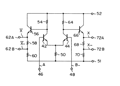
Fig. 5 is a schematic diagram of a logic circuit
according to an embodiment of the present invention in which
transistors 42 and 44 comprise a pair forming a differential
amplifier. A first input terminal 46 receives a first
binary input signal A that is fed to the base circuit of
transistor 44, and a second input terminal 48 receives a
second binary input B- and that is fed to the base circuit
of second transistor 44. The constant current source is
provided by resistor 50 that is connected between the common
emitter connection of transistors 42 and 44 and a common or
return line having terminal 51. The collector circuit of
transistor 42 is connected to the appropriate source voltage
terminal 52 through a resistor 54, and the collector circuit
of transistor 42 iB also connected to the base lead of an
emitter-follower trans$stor 56. Emitter-follower transistor
56 has its emitter lead connected through series-connected
resistors 58 and 60 to the common or return line having
terminal 51 and one output terminal 62a (X) i~ connected at
_g_
~27772~ S03003
the connection point of the emitter lead of emitter-follower
transistor 56 and resistor 58 and a second output (X-) is
obtained from output terminal 62b at the connection point
between resistors 58 and 60.
The collector circuit of transistor 44 is
similarly connected to voltage source terminal 52 through
resistor 64 and is also connected to a base lead of output
transistor 66 that is connected in the emitter-follower
configuration. Transistor 66 has emitter resistors 68 and
70 connected in series to the return line that can be
connected at terminal 51 to electrical ground potential.
Another output signal X is obtained at the connection
between the emitter lead of transistor 66 and resistor 68 at
terminal 72A, and the output X- may be obtained at terminal
72 connected at the node between resistors 68 and 70. As
will be seen from the circuit of Fig. 5, resictors 60 and 70
comprise constant current source resistors for output
transistors 56 and 66, respectively. Because this is a
logic circuit having outputs and inputs that are balanced,
resistors 54 and 64 will have the same values and,
similarly, resistors 58 and 68 will also have the same
values. The values of resistors 60 and 70 are selected so
that the constant current provided thereby will have a
magnitude approximately 1/2 that of the constant current
provided by resistor 50.
The operation of the circuit of Fig. 5 is
represented by the relative voltage levels of F~g. 6, in
which inputs A and B- have the same amplitude differences VL
between the high and low levels. Compared with input A,
--10-- -
. ~27772.~J S03003
input B- has levels of H- and L-, which are shifted by an
amount 1/2 Vl from levels H and L, respectively. Thus, the
rela~ionships between resistors 60, 70, and 50 are seen. In
regard to the absolute voltage levels, assuming that the
source voltage applied at input terminal 52 is Vcc, and the
voltage drop across the base and emitter of a transistor is
VBE, then the relative levels are seen as follows:
H = Vcc - VBE
L = Vcc - VBE - VL
H- = Vcc - VBE - 1/2 VL
L- z Vcc - VBE - VL - 1/2 VL
For example, assuming that A = L and input B- ~
L-, then transistor 42 is turned ON and transistor 44 is
tuxned OFF and a constant current I flows through transistor
42. The collector potential of transistor 42 then becomes
(Vcc - IR), when the resistance value ~f resistor 54 is
represented by R. Thus, output X present at output terminal
72A becomes (Vcc - IR - VBE) and, accordingly, when IR z VL,
output X becomes L and because the resistance value of
resistor 58 is selected as R and because the constant
current due to resistor 60 is set tc be 1/2 I, output X- at
output terminal 72B will become (Vcc - IR - VBE - 1/2 VL
h-).
Continuing with this example, the collector
voltage of transistor 44 will be Vcc and the output X at
terminal 72A will be (Vcc - VBE = H), whereas output X- at
terminal 72B will be ~Vcc - VBE - 1/2 VL = H-). The
relationships between the levels of the inputs and outputs
--11--
~ .~777~.7 S03003
are seen to be identical, thereby preventing a potential
troublesome problem when a plurality of such logic circuits
are connected.
The relationships between the inputs and outputs
in the embodiment of Fig. 5 relative to positive logic
circuit are represented by the following table:
A B- X X- X X-
. ._
L L- H H- L L-
L H- L L- H H-
H L- H H- L L-
H H- H H- L L-
The logic circuit provided by the embodiment of
Fig. 5 is &hown in conventional circuit design notation in
Fig. 7. ~oreover, in the practical situation both the
positive output and negative output can be obtained and the
fundamental logic circuits represented as AND, NAND, OR, and
NOR can be realized by selecting from among the outputs X,
X-, X, and X-. In further embodiments of the present
invention, in order to obtain the desired level shift of 1/2
VL, the constant current source may be connected to the
emitter of two emitter-follower configuration transistors or
a circuit arrangement as represented in Figs. 8 and 9 may be
employed.
Referring then to Fig. 8, ~he collectors of
transistors 42 and 44 are connected through collector
resistors 54 and 64, respectively, that are connected in
~ ~7772~ S03003
common to a current source resistor 76 having a magnitude
selected as 1/2 R, based on resistor 54 being assigned the
value R. Resistor 76 is then connected to the power source
input at terminal 52. In the circuit of Fig. 8, output X-
and X- having levels H- and L- can be obtained at output
terminals 62B and 72B, respectively.
Similarly in Fig. 9, by connecting the emitter of
the emitter-follower configuration transistors 56 and 66 to
resistors 58 and 68, respectively, connected to the common
line and connecting terminal 51 to ground, providing a
resistor 78 as a constant current source between the
collector of transistor 44 and the grounded return line, and
by ~electing the constant current t~at flows through
resistor 78 to be 1/2 I, the oùtput X can be obtained at
terminal 62A and the output X- can be obtained at output
terminal 72B.
Another embodiment of the present invention that
can accept four binary input signals i8 shown in Fig. 10 in
which transistors 42, 44, and 80, 82 comprise a differential
amplifier, a first input A applied at terminal 46 is
connected to the base lead of transistor 42 and a second
input B supplied at terminal 84 is applied to the base lead
of transistor 80. A third input C- is supplied at terminal
48 and applied to the base lead of transistor 44 and a
fourth input D- is supplied at terminal 86 and is fed to the
base lead of fourth transistor 82. The collectors of
transistors 42 and 80 are connected in common to the base of
emitter-follower output transistor 56 and are also connected
through resistor 54 to the voltage source at terminal 52.
Output terminal 62A provides X taken from the emitter lead
-13-
S03003
~.27772t~
of emitter-follower transistor 56, and the collector leads
of transistor 44 and 82 are connected in common and at such
connection point the base lead of output transistor 66 is
connected. The common collectors of transistors 44 and 82
are then connected through resistor 64 to the voltage source
at terminal 52. Output X is taken off at the emitter of
transistor 66 at terminal 72A.
In order to better represent the relationships
among the voltage levels of the four inputs and two outputs
of the circuit of Fig. 10, attention is directed to Fig. 11,
in which inputs A and B are binary signals each having
possible amplitude levels L and H and inputs C- and D- are
also binary signals having possible amplitude levels L- and
H-. The signals A and B have the same logic amplitude, as
do the binary ~ignals C- and D-. Additionally, there i8 a
difference of 1/2 VL between the corresponding levels of the
pair of signals A and B and the pair of ~ignals C- and D-.
When the embodiment of Fig. lO is represented as
employing positive logic, the functional equivalent of the
logic circuit of Fig. 12 can be obtained. The corresponding
relationship between the inputs and outputs of the circuit
of Fig. 12 may be easily determined from the following
table.
A B C- D- X X
L L L- H- L H
L L H- L- L H
L L H- H- L H
L H H- H- H L
R H L
1~7772.?J
S03003
Other combinations of inputs that are not shown in
the above table are also possible, in which for example, X =
H and X = L. That is, when both of the inputs A and B are
at level L and either one of inputs C- and D- is at level H-
transistors 42 and 80 are turned OFF and either one of
transistors 44 and 82 is turned ON, so that X = L and X = H.
This logic relationship is, of course, different from the OR
and NOR functions which are obtainable using conventional
emitter-coupled logic.
As indicated hereinabove, the present invention
can also provide in addition to the above described logic
elements an R-S flip flop. Such flip flop being of the kind
known in the prior art and shown in Fig. 4 as typically
comprising two "NOR" gates. Referring back to Fig. 4 it is
seen that a conventional R-S flip flop can be con~tituted by
two ECL NOR gates and a ~et input S i~ supplied to an input
of one NOR gate, a reset input R is supplied to one input of
the other NOR gate, and the outputs of the two NOR gates are
connected to the remaining inputs of the respectively
opposite NOR gates, with the outputs of the two NOR gates
representing the circuit outputs. In conventional
emitter-coupled logic, each of the NOR gates of the prior
art R-S flip flop of Fig. 4 is embodied in accordance with
the circuit of Fig. 1 and requires an input reference
voltage and a reference voltage transistor.
An R-S flip flop can be realized according to the
present invention by combining two of the logic circuits as
shown in Fig. 12 in the manner shown in Fig. 1~. In which
case, two set inputs Sl and S2 are fed to one OR gate and
two reset inputs R1 and R2 are supplied to the other OR
-15
1.27772.~ S03003
gate. An output Q- of one logic circuit is supplied to
another of the OR gates of the embodiment of Fig. 12, as is
the output Q- from the other logic circuit. Accordingly, it
i8 ~een that in this fashion an R-S flip flop is easily
constituted.
An equivalent representation of the circuit of
Fig. 13 is shown in Fig. 14 in which the NOR gates
comprising the flip flop are represented in general by a
flip flop F/F, and the remaining input OR gates are
connected to the set input S and reset input R of the R-S
flip flop F/F. Therefore, the present invention is quite
suitable for applicationg involving a plurality of set
inputs or reset inputs fed to a flip flop.
The circuit of Fig. 13 is shown in more detail in
Fig. 15 in which one logic circuit is formed of transistors
42, 80, 44, and 66, while the other logic circuit i8
provided by transistors 88, 90, 92, and 94. Transistors 42,
80, and 44 comprise a differential amplifier in which one
set input Sl supplied to terminal 46 is connected to the
base-lead of transistor 42 and the other set input S2
supplied at input terminal 84 is supplied to the base lead
of transistor 80. Similarly, a second differential
amplifier is comprised of transistor 88, 90, and 92 and a
first reset input R1 supplied to input terminal 94 is
applied to the base lead of transistor 88 and a second reset
input R2 supplied to input terminal 96 i8 applied to the
base lead of transistor 90. A constant current similar to
that provided by resistor 50 is provided by resistor 97.
The collector output of transistor 44 is connected to the
base lead of a emitter-follower transistor 66 and is level
-16-
~.~777Z.~ S03003
shiftecl by operation of emitter resistor 68 and is also
connected to the base lead of transistor 92. Similarly, the
collector output of transistor 92 is fed to the base lead of
an emit:ter-follower transistor 94, is level shifted by
re~istor 98, and is fed to the base lead of transistor 44.
The output Q- is then obtained at the node between
emitter-follower resistors 68 and 70 and the output Q- is
obtained at the node between emitter-follower resistors 98
and 100. These outputs could also be obtained directly at
the emitter lead of transistors 66 and 94, respectively, in
which case the level of each output would be larger by 1/2
VL than the outputs that would be obtained in the circuit of
Fig. 15.
The timing of the R-S flip flop of Fig. 15 is
shown in Fig. 16 in which it is ~een that when the set input
Sl or S2 rises from lower level L to the higher level H, the
flip flop is reset and transistor 42 or 80 is turned ON and
transistor 44 is turned OFF. Accordingly, output Q- will
rise from the low level L- to a relatively higher level H-
and transistor 92 in the second differential amplifier will
be turned ON and transistor 88 and 90 in such differential
amplifier will be turned OFF. Thus, output Q- falls from
the relatively high level H- to the lower level L-. This
state will be held then even if the set input Sl or S2 falls
to a low level L. When the reset input Rl or R2 rises from
the low level L to the high level H in the set state,
transistor 88 or 90 in the second differential amplifier is
turned ON and transistor 94 i6 turned OFF. Thus, output Q-
rises from the relative low level L- to the relative high
level H- and transistor 44 of the first amplifier is turned
-17-
~27'7'~2 S03003
ON and transistors 42 and 80 are turned OFF, there~y output
Q- falls from high level H- to the low level L-. It is seen
then that this reset state will be held even if the reset
input R1 or R2 assumes the low level L.
Another embodiment that is pos6ible according to
the present invention that is similar to that shown in Fig.
13 i8 shown in Fig. 17. In the R-S flip flop of Fig. 17, a
set input S- and a set input control signal A- are supplied
to the inputs of a NOR gate of one of the logic circuits,
while a reset input R- and a reset input control signal B-
are supplied to a NOR gate of the other of the two logic
circuits. This can be equivalently shown in Fiq. 18 in
which the two NOR gates are connected respectively to the
set input and reset input of the R-S flip flop (F/F), and
such flip flop is operat$ve only by the inputs that are
supplied to the two respective NOR gates.
More 6pecifically, the set input S- can pass
through first NOR gate only when the set input control
signal A- is at the low level L- and the reset input R- can
pass through the other NOR gate only when the reset input
control signal B- is at the low level L-. In this way, the
R-S flip flop of the so-called clock synchronization kind
can be realized by providing such prohibition gates. In the
conventional prior art arrangement, four differential
amplifiers are required because the R-S flip flop and the
NOR gates must be individually constituted. Nevertheless,
according to the present invention the R-S flip flop of the
so-called clocksynchronization kind can be comprised of a
relatively few number of circuit elements.
1~77722 S03003
Fig. l9 shows the circuit diagram of an R-S flip
flop that corresponds to the arrangement shown generally in
Fig. 18, in which one logic circuit is comprised of
transi~tors 42, 80, 44, and 66 and the other logic circuit
is comE~rised of transistors 88, 90, 92, and 94. More
specifically, one differential amplifier consists of
transistor 42, 80, and 44 and the set input S- supplied at
terminal 46 is fed to the base lead of transistor 42, and
the set input control signal A- supplied to input terminal
84 is connected to the base lead of transistor 80. A second
differential amplifier is made up of transistors 88, 90, and
92 and the reset input R- supplied to input terminal 94 is
connected to the base lead of transistor 88 and the reset
input control signal B- supplied to input terminal 96 is
connected to the base lead of transistor 90. The collector
output of transistor 44 is fed to the ba~e lead of an
emitter-follower transistor 66 and the emitter output
thereof i5 supplied to the base lead of transistor 92.
Similarly, the collector output of transistor 92 is fed to
the base lead of a second emitter-follower transistor 94 and
the output thereof is fed to the base lead of transistor 44.
Therefore, the output Q is obtained from the emitter circuit
of transistor 66 and the output Q is obtained from the
emitter circuit of transistor 94. A constant current source
to provide the inventive level shifting may be connected to
the emitters of transistors 66 and 94, and the outputs
having levels that are smaller by an amount 1/2 VL than the
above described outputs Q and Q can be obtained.
--19--
~ ~777Z~ S03003
The timing of the circuit of Fig. 19 is
represented in Fig. 20, in which it is seen that when the
set input S- that is fed in through input terminal 46 to the
base of transistor 42 falls from the relatively high level
H- to the relatively low level L- and the flip flop is reset
and when the set input control signal A- is at the low
level, transistors 42 and 80 are turned OFF and transistor
44 is turned ON, because the level L- is lower than the base
potential L of transistor 44. Thus, output Q falls from the
high level H to the low level L and transistor 92 of the
second differential amplifier is turned OFF and transistors
88 and 90 are turned ON, whereby output Q rises from the low
level L to the high level H. This state is the set state
and is held even if the set input S- or set input control
~ignal A- assumes the high level. When the reset input R-,
which is fed in through input terminal g4 to the base of
transistor 88 falls from the relatively high level H- to the
low level L- in the set state and when the reset input
control signal B- is at the low level L-, transistors 88 and
90 are turned OFF and transistor 92 is turned ON, because
the level L- is lower than the base potential L of
transistor 92. Thus, the output Q falls from the high level
H to the low level L and transistor 44 of the first
dlfferential amplifier is turned OFF and transistors 42 and
80 are turned ON, whereby output Q rises from the low level
L to the high level H. This reset state will be held even
if the reset input R- or the reset input control signal B-
assumes the high level H.
-20-
~.~2~ S03003
As may be seen then from the timing chart of Fig.
20, the R-S flip flop of Fig. 19 can be used as the
so-cal:Led clock-synchronization R-S flip flop if the set
$nput control signal A- and the reset input control signal
B- are formed by a common clock input signal CK-. This
configuration is represented schematically in Fig. 21.
A further example of an R-S flip flop that may be
constituted using a single logic circuit according to the
present invention is shown in Fig. 22. More particularly, a
set input S can be supplied to both inputs of an OR gate,
the reset input R- supplied to one input of a NOR gate, and
the outputs of the OR gate and the NOR gate are both
supplied to respective inputs of a second NOR gate. The
output of such second NOR gate iB then supplied as the
second input to the first NOR gate, to which the reset input
R- was supplied. In order to realize the configuration of
the circuit of Fig. 22 a schematic of an embodiment of the
present invention is shown in Fig. 23, in which transistors
44 and 82 comprise differential amplifiers and the
collectors of these differential amplifiers are connected
together. The set input S then is supplied to input
terminal 46 and applied to the base lead of transistor 42
and the reset input R- supplied to input terminal 48 is
applied to the base lead of transistor 44. The collector
circuit of transistor 42 is connected to the voltage source
at terminal 52 through a collector resistor 54, and the
collector of transistor 42 is also connected to the base
lead of output transistor 56, which is connected in the
emitter-follower configuration. The emitter of transistor
56 is connected to the return line, which i6 connected at
-21-
127772.~ S03003
terminal 51 to relative ground potential, through
series-connected resistors 58 and 60. At the node of
resistors 58 and 60 is connected the base lead of transistor
BZ and at this point also the output Q- is also obtained.
It shou:Ld also be noted that the output could be taken
directly from the emitter lead of transistor 56, and this
will involve the appropriate voltage level shift.
The operation of the R-S flip flop circuit of Fig.
23 is represented in the timing chart of Fig. 24, in which
it is seen that when the set input S rises from the low
level L to the high level H while in the reset state, the
output Q- is at the relatively high level H-, and transistor
42 is turned ON and transistors 44 and 82 are turned OFF,
because the high level H is greater than the relatively high
level H-. Thus, the output Q- fall~ from the relatively
high level H- to the lowest level L-, and ~hereafter this
state is held even if the set input S assumes the low level
L. When the reset input R- rises from the lowest level L-
to the relatively high level H- during the set state,
transistor 44 is turned ON and transistor 42 is turned OFF,
because the relatively high level H- is greater than the low
level L. Therefore, output Q- rises from the lowest level
L- to the relatively high level H- and, thereafter, this
state will be held even if the reset input R- assumes the
low level L.
Referring back to the R-S flip flop circuit of
Fig. 23, because this flip flop uses a single differential
amplifier as the fundamental constructional element, the
number of elements is minimized and, therefore, time delay
-22-
1~7772,~ S03003
due to collector capacitance of the transistors and the like
is also held correspondingly small and, thus, the circuit of
Fig. 23 provides high-speed operation.
A still further example of the present invention
in which an R-S flip flop can be provided having multiple
inputs and multiple outputs is shown in Fig. 25. In the
circuit o Fig. 25, one differential amplifier is formed of
two transistors 42 and 80 and the input signal S} supplied
at terminal 46 is applied to the base lead of transistor 42
and the other set input S2 supplied at input terminal 84 is
applied to base lead of transistor 80. The collector leads
of these two transistors forming the first differential
amplifier are connected together in the known fashion. The
second differential amplifier is formed from transistors 44
and 80 and reset input ~ignal Rl- ~upplied at input terminal
48 is fed to the base lead of transistor 44 and the second
reset signal R2- supplied to terminal 86 is fed to the base
lead of transistor 82. Again, as in the conventional
differential amplifier configuration, the collectors of
transistors 44, 82, and 100 are connected together. The
collector node of transistors 42 and 80 is connected to the
power source input terminal 52 through resistor 54 and this
collector node is also connected to the base lead of
transistor 56 that is connected in the common-emitter
configuration. More specifically, the emitter lead of
transistor 56 is connected to relative ground potential at
terminal 51 through series resistors 58 and 60. The
collector node of transistors 44, 82, and 100 is connected
to the power source terminal 52 through resistor 64, and
this common collector node is also connected to the base
-23-
lZ7772.~
S03003
lead of emitter-follower transistor 66. The emitter of
transistor 66 is connected to relative ground potential
through a series connection of resistors 68 and 102. The Q-
output is available at the node between resistors 58 and 60
of emitter-follower transistor 56 and this point is also
connected to the base lead of transistor lO0, which is part
of the second differential amplifier. The output terminal
72A at which output Q is available is connected directly to
the emitter of transistor 66, and the Q- output at terminal
72B is taken off at the node between series resistors 68 and
102. The R-S flip f}op of Fig. 25 provides substantially
the same operation is that of the R-S flip flop of Fig. 23
and is functior.ally represented in Fig. 26. Thus, in using
the embodiment of Fig. 25, two outputs Q and Q- having a
level difference of 1/2 VL are obtained.
Throughout the above embodiment~, although a
resistor or resistor combination has been employed as a
constant circuit source, a constant current source arranged
to apply a predetermined DC voltage between the base and
emitter of the appropriate transistors could be utilized as
well.
Although illustrative embodiments of the present
invention have been described in detail above with reference
to the accompanying drawings, it i8 to be understood that
the invention is not limited to those precise embodiments,
and that various changes and modifications can be effected
therein by one skilled in the art without departing from the
spirit and scope of the invention, as defined by the
appended claims.
-24-