Note: Descriptions are shown in the official language in which they were submitted.
~277 77~
PROCESS FOR MANUFACTURING THERMAL INK JET PRINTHEADS
AND INTEGRATED CIRCUIT (IC) STRUCTURES PRODUCED THEREBY
Technical Field
This invention relates generally to thermal ink
iet printhead construction and more particularly to an im-
proved integrated interconnect circuit extending between the
printhead heater resistors and external pulse drive circuit-
ry for supplying drive current to these heater resistors.
Backqround Art
In the manufacture of thin film resistor (TFR)
type of ther~al ink jet printheads, it is a common practice
to photolithographically define the individual heater resis-
tors on a TFR substrate by creating a pattern in an over-
lying conducting trace layer. This layer is deposited in a
predetermined pattern on the resistive heater material using
known deposition techniques, The resistive heater layer
material may, ~or example, be tantalum-aluminum, TaAl. The
conductive trace pattern is most typically aluminium, al-
though it could also be gold or other conductive material
compatible with the other materials in the materials set for
the printhead. After the conductive trace material or pat-
tern is completed, it is then usually covered with an inert
barrier layer such as a composite layer of silicon nitride
and silicon carbide in order to protect the underlying
layers from cavitation wear and ink corrosion.
In order to make electrical contact between this
conductive trace material and external pulse drive circuitry
for the printhead, one standard prior art approach involved
etching a relatively large opening or via in the silicon
nitride/silicon carbide composite barrier layer and then
forming a relatively large contact pad in this opening to
thus make contact with the underlying aluminum trace con-
ductor material. Then, wire bonding or pressure contact
connections could be made to this relatively large contact
pad to provide an electrical current path into the aluminum
trace material and to the ink jet heater resistors.
The above prior art structure is possessed with
several disadvantages associated with the relatively large
opening or via in the insulating barrier layer and directly
over the aluminu~ conductlve trace layer. Tho ~irst of
these disadvantages re~ides in the ~act that the large via
in the silicon nitride/silicon carbide composite layer ex-
poses a relatively large sidewall area of these materials.
This large area sidewall exposure means increasing the area
in which pinholes or cracks might possibly occur and thus
produce electrical shorts in the barrier layer. As a result
of the dissimilarity of the silicon nitride and silicon
carbide layers and the differences in their etch rates,
there is produced a "diving board" geometry at the edge of
these two dissimiliar insulating materials at the via open-
ing. This stepped geometry, when coupled with the large
area deposited contact pad in the via, increases the proba-
bility of material defects in this region which are capable
1277774
of reducing wafer processing yields.
Another disadvantage of the above prior art elec-
trical interconnect approach involves exposing a relatively
large area of the aluminum trace material in order to pro-
vide the desired wide area contact pad thereover. The
exposure of such a large area of aluminum trace material in
the manufacturing process increases the possibility of form-
ing aluminum oxide, A1203, on the conductive trace material
and thus rendering it insulating or partially insulating
instead o~ fully conducting.
Another disadvantage of using the above prior art
approach resides in the increased probability o~ undercut-
ting the silicon nitride and silicon carbide layers during
the etching of the via therein. Again, such increased
probability is caused by the expo8ure 0~ the relatively wide
area sidewall o~ the silicon nitride/silicon carbide barrier
defining the via.
Another disadvantage of using the prior art ap-
proach described above relates to the ~ormation o~ a non-
flat dish-shaped contact pad directly over the aluminum
trace material. ~his geometry and structure increases the
likelihood of scratching the edge of the printhead structure
immediately ad~acent the conducting trace material, and such
scratching in turn increase~ the likelihood of producir.g
electrical shorts down through the printhead structure to
the aluminum conductive trace material. In addition, the
dish shape or non-planar contour of the contact pad makes it
1277774
difficult to make certain types of electrical connections to
the printhead structu~e, e.g. spring biased pressure connec-
tions from a lead frame-type of flexible circuit.
A further disadvantage of using the above prior
approach relates to the sensitivity o~ chipping and cracking
at the edges of the multiple layers of materials over which
the dish-shaped contact is placed. This chipping and crack-
ing will cause corrosion of these materials at their outer
edges, but this does not occur in devices manufactured by
the present invention where the lead-in contacts have been
removed from pressure contact at the edges of these interior
layered materials.
~i~çLQ~yL~Lof Invention
The general purpose of this invention is to pro-
vide a new and improved integrated circuit interconnect
structure for providing drive current to thermal ink jet
printhead heater resistors and a high yie}d process for
fabricating same. This interconnect structure is uniquely
adapted and constructed for making good electrical connec-
tions to spring biased pressure contacts, such as individual
fingers or leads on a lead frame type of flexible or "flex"
circuit.
To accomplish this purpose, I have discovered and
developed a pr$nthead structure and fabrication process
therefor which includes forming a resistive layer on an
insulating substrate and then ~orming a conductive trace
pattern laterally coextensive with the resistive layer and
12777~,g
extending only over a predetermined area of the
insulating substrate. The conductive trace pattern has
an opening therein defining a resistor heater element.
Next, an insulating barrier layer is formed atop the
conductive trace material and extends down over the
edges of the conductive trace material and the resistive
layer and then out over a predetermined area of the
adjacent insulating substrate. Then, a small via is
formed in the insulating barrier layer and over the
conductive trace pattern, so that a subsequently
deposited metal overlay pattern may be extended from
into the via and then out over the adjacent area of the
insulating substrate where no conductive trace material
extends. In this manner, the interconnect metal in this
latter area provides a relatively large and flat
electrical contact area for spring biased contacts.
And, the electrical connection to the conductive trace
pattern is only through the relatively small via in the
barrier layer where the area o~ edge expo~ure in the
barrier layer and the area of conductive trace material
exposure is mainted at a minimum.
Various aspects of the invention are as follows:
A proces~ for fabricating a thin film resigtor
printhead structure which includes:
a. forming a resistive layer on an
insulating substrate and a conductive trace
pattern located on the resistive layer and having
an opening therein defining a resistive heater
element,
b. forming an insulating barrier layer atop
said conductive trace pattern,
c. forming a via in said insulating barrier
layer for receiving a metal overlay pattern in
electrical contact with said conductive trace
pattern, said via having a geometry which exposes a
1Z7~774
6A
predetermined area of said conductive trace pattern
and
d. extending said metal ovèrlay pattern
from said conductive trace pattern and through
said via and down over an adjacent area of said
insulating substrate, whereby the metal overlay
pattern over said adjacent area of said insulating
substrate provides a rèlatively large and flat
electrical contact area remote from said conductive
trace pattern for receiving a spring biased
contact.
A thin film resistor printhead and interconnect
structure including, in combination:
a. a resistive layer and a conductive trace
pattern formed on a predete~mined area of an
insulating substrate, and said conductive trace
pattern having an opening therein de~ining a
resistive heater element,
b. an insulating barrier layer formed atop
said conductive trace pattern and having a surface
geometry which expose~ a predetermined area of said
conductive trace pattern, and
c. a metal overlay pattern extending from
said conductive trace pattern and down over and on
an adjacent area o~ said insulating substrate under
which no conductive trace pattern appears, whereby
the metal over said adjacent area of said
insulating substrate provides a relatively large
and flat electrical contact area for receiving a
spring biased contact.
A thin film interconnect structure including, in
combination:
a. a resistive layer and a conductive trace
pattern formed thereon disposed on a predetermined
area of an insulating substrate, and said
;~,
1m7~4
6B
conductive trace pattern having an opening therein
defining a resistive transducer element,
b. an insulating barrier layer formed atop
said conductive trace pattern and having a surface
geometry which exposes a predetermined area of said
conductive trace pattern, and
c. a metal overlay pattern extending from
said predetermined area of said conductive trace
pattern and down over and on an adjacent area of
said insulating substrate under which no conductive
trace pattern appears, whereby the metal on said
adjacent area of said insulating substrate provides
a relatively large and flat electrical contact area
for receiving an electrical contact.
The above and other advantages, novel features and
alternative methods of construction of this invention
will become better understood in the following
description of the accompanying drawings.
~ie~ ri~~ ~8
Figure~ 1 through 7 illustrate, in schematic views,
a series of thin ~ilm resistor process steps uti-
;::
',` ~
12~m4
lized in fabricating a printhead interconnect structure
according to the invention.
Figure 8 is an alternative embodiment of the in-
vention wherein the barrier layers have been laterally re-
duced to expose an edge portion of the underlying aluminum
trace material for subsequent metal overlay thereon.
Be$t ~ode For Carrying Out The Invention
Referring now to Figure 1, a substrate starting
material 10 such as silicon is treated using either thermal
oxidation or vapor deposition techniques to form a thin
layer 12 o~ silicon dioxide thereon. The combination of th~
silicon substrate lO and the layer 12 of silicon dioxide
will be re~erred to herein as the "insulating substrate"
upon which a subsequent layer 14 o~ resisltive heater
material is depo~ited. Pre~erably, the layer 14 will be
tantalum aluminum, TaAl, which is a well known resistive
heater material in the art ot thermal ink jet printhead
construction. Next, a thin layer 16 of aluminum is depos-
ited atop the tantalum aluminum layer 14 to comp}ete th~
structure o~ Figure 1.
In the particular materials set described above
for a preferred embodiment o~ the invention, the silicon-
silicon dioxide combination 10, 12 was approximately 600
microns in thickness; the tantalum aluminum layer 14 was
approximately 1000 angstroms in thickness; and the aluminum
conductive trace material 16 was approximately 5000 ang-
stroms in thickness. The resistor and conductor materials
~2~774
were magnetron sputter deposited. This materials set is
generally well known in the art and is described, for
example, in the Hewlett-Packard Journal, Vol. 36, No. 5,
May, 1985.
Referring now to Figure 2, the structure shown
therein was appropriately masked and etched with a
suitable etchant in order to define the composite island
18 of tantalum aluminum 14 and aluminum 16 on the right
hand side of the insulating substrate. As will become
better appreciated below, the island 18 is formed on
only a portion of the insulating substrate 10 and 12,
leaving an area of the left-hand side of the substrate
available for making good electrical contacts of the
type to be described. Next, as shown in Figure 3, a
pattern is etched in the aluminum layer 16 to form the
opening 20 which define~ the lateral extent of a
re~istive heater element 22 which i~ current driven by
the conductive trace aluminum layer 16.
Next, as shown in Figure 4, a composite layer
barrier material is deposited over the upper surface of
the structure in this figure and includes a first layer
24 of silicon nitride which is covered by a second layer
of highly inert silicon carbide. This composite layer
(24, 26) barrier material provides both good adherance
to the underlying materials and good insulation and
protection against cavation wear and ink corrosion which
the underlying layers beneath these materials 24 and 26
would otherwise receive during an ink jet printing
operation.
127'm4
Next, as shown Figure 5, a relatively small via 28
is dry etched in the composite silicon nitride/silicon car-
bide barrier layer using freon gas to thereby leave a small
area 30 in the aluminum conductive trace material exposed
for ~urther electrical contact. Such contact is made as
shown in Figure 6 when a conductive lead-in or overlay
pattern of conductors 32 and 34 are magnetron sputter
deposited on the surface of Figure 5 and extend from into
electrical contact with a relatively small area 30 of con-
ductor trace material and then out onto the left hand side
o~ the structure in Figure 5 and atop the previousl~
deposited barrier layer material. The combined thic~ness of
the gold and tantalum layer~ is approximately 2 microns.
Thi~ conductivs lead-in compositQ structure in-
cludes a ~ir~t layer 32 of tantalum and a second layer 34 of
gold successively deposited in the geometrical configuration
shown using conventional masking and metal evaporation tech-
niques. Thus, the area 36 on the upper sur~ace of the gold
layer 34 in Figure 6 extends over a relatively wide and
flat area of the integrated structure and is located away
from the aluminium conductive trace pattern previously de-
scribed. Thia construction therefore enables a finger or
spring lead contact member 38, which may be part of a larger
lead frame member (not shown), to be brought into good ~irm
pressure contact with the sur~ace area 36 o~ the gold layer
34 and without causing any detrimental ef~ect on the alumi-
num conductive trace pattern. This larger lead frame member
1277774
is described in more detail in U.S. Patent No. 4,806,106
of Janet E. Mebane et al issued February 21, 1989 and
assigned to the present assignee.
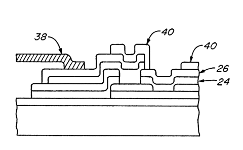
Finally, and of course prior to the
application of the spring biased contact 38, a surface
pattern of polymer material 40 is formed in the geometry
shown in Figure 7 to a thickness of approximately 50
microns. This polymer material provides a protective
layer or shield over the contact via 30 and over the
electrical contact layers 32 and 34 extending down into
contact therewith.
It will be understood that, for sake of
brevity, only a single heater resistor and conductive
trace connection therefor has been shown. However, in
actual practice the printhead will have many of these
heater resistors which will usually be symmetrically
spaced in a rectangular pattern on one area of the
insulating substrate.
Various modification~ may be made in the above
described embodi~ent without departing from the scope of
this invention. For example, in Figure 4, it may be
preferable in certain applications to deposit layers 24
and 26 on only a predetermined area of the underlying
aluminum trace material 16. Then, the tantalum and gold
layers 32 and 34 would be deposited over an area of edge
exposed aluminum trace material and down and out over
the now-exposed silicon dioxide layer 12 on the left
hand side of the device structure. Thus, in this
modified embodiment as shown in Figure 8, the tantalum-
gold composite layer 32', 34' on the now-exposed left
; hand sio2 layer 12 will serve as the electrical contact
area for receiving the above spring biased leads or the
like. The Si3N4/Si C composite layer 24', 26' is masked
and etched so as to leave a small edge portion of the
aluminium trace material 16' exposed to receive the
tantalum layer 32' thereon as shown in Figure 8. And,
. ~
1277774
as in Figure 7, there is a relatively wide area on the
surface of the gold film 34' for receiving the spring
biased lead contact 38'. Finally, and also as in Figure
7, the outer layer 40' in Figure 8 corresponds to the
surface protection polymer layer 40 as indicated above
with respect to Figure 7.
Industrial Ap~licability
The present invention is used in the
fabrication of printheads for thermal ink jet printers
which serve as standard peripheral equipment for a
variety of computers and the like.