Note: Descriptions are shown in the official language in which they were submitted.
~.27~2~
This invention relates to a power supply for an arc
lamp, and is particularly concerned with a power supply of
the general type comprising a power source and an
inverter. The arc lamp is typically a metal halide lamp
of the type used for cinematographic and television
lighting.
An arc lamp of this type is preferably driven by
alternating square wave current so as to avoid modulation
of the light output at the supply frequency as would occur
if the current supply were sinusoidal. Attempts have been
made to achieve a satisfactory square wave output for this
purpose.
~;~
Canadian Patent No. 1185649 dated April 16, 1985, in
the name Lee Electric (Lighting) Limited, discloses a
power supply for arc lamps which represents a notable
advance over the prior art. The power supply is designed
to deliver alternating square wave curr2nt for driving an
arc lamp, but is more compact and more convenient to use
than the power supplies previously used. The power supply
essentially comprises a power source feeding an inverter
from which the output current is derived, the power source
being a constant current source comprising a rectifier, a
capacitor, an inductor and a field effect transistor
connected in series~ The inverter is connected across the
capacitor so that current supplied to the inverter is
is drawn through the field sffect transistor. The
constant current source is maintained by means of a
chopper oscillator for controlling the conduction of the
field effect transistor in response to the current drawn
by the field effect transistor. The inverter comprises a
bridge network of field effect transistors driven by a
bridge oscillator to deliver the current output at the
required output frequency~
While the power supply disclosed in the above
Canadian patent is an improvement over the earlier power
supplies, it also has shortcomings. One shortcoming is
that the constant current source and the inverter are
necessarily controlled by separate oscillators and in
consequence the system cannot be truly synchronous. While
the lack of synchronism in the system does not
necassarily affect the light output adversely, it gives
rise to noisy operation. Another shortcoming is that,
since th~ power source is controlled by the chopper
oscillator to give a constant current output, it cannot
provide a constant power output since the voltage is
subject to variation. This is a disadvantage because
variations in the power level give rise to variations in
the quality and spectral distribution of the light output.
The present invention overcomes the above-mentioned
disadvantages by providing a power supply which is
synchronous and in which the current source is controlled
so as to operate the arc lamp at a constant power level,
thereby ensuring a constant quality of the light output
over the operating range of voltage.
Accordingly, the invention provides a power supply
for an arc lamp comprising a power source and an inverter,
in which the power source comprises a rectifier, a
capacitor, an inductor and a switching transistor
~l~7~
3 --
connected in series, and the inverter comprises a bridge
network of field effect transistors, the bridge network
being in parallel with the capacitor so that current
supplied to the inverter is drawn through the switching
transistor. The bridge network is controlled by a timing
circuit comprising a master clock, means for deriving from
the master clock a sequence of square wave pulses at a
first selected reference frequency, and means for deriving
from said sequence of pulses a pair of complementary
sequences of square wave pulses at a second selected
reference frequency which is a submultiple of the first
for driving the field effect transistors of the inverter
selectively in pairs. The power source is controlled by a
PWM circuit which is responsive both to current drawn by
the switching transistor and voltage applied to the bridge
network for controlling conduction of the switching
transistor so as to maintain the output of the inverter at
a substantially constant power lev~l. This PWM circuit
comprises a pulse generator controlled by the master clock
for generating a sequence of control pulses at said first
reference frequency, a first feedback circuit responsive
to current drawn by the switching transistor for deriving
a current-responsive first signal, a second feedback
circuit responsive to voltage applied to the bridge
network for deriving a voltage-responsive second signal,
comparator means for comparing the first and second
signals to derive a difference signal, means for gating
said control pulses with the difference signal to derive
PWM pulses at said first reference frequency, and control
circuit means for controlling the conduction of the
switching transistor in a PWM mode in accordance with the
derivation of the PWM pulses.
One embodiment of the invention will now be
described, by way of example, with reference to the
3~ accompanying drawings. In the drawings:
"` ~L27~
Figure 1 is a block diagram showing the four
principal sections of the power supply;
Figures 2a and 2b together form a detailed wiring
diagram of the power supply;
Figure 3 is a schematic block diagram of the power
circuitry, represented by a single block in Figure 1;
Figure 4 is a schPmatic block diagram of the
inverter drive circuitry, represented by a single block
in Figure 1;
Figure 5 is a schematic block diagram of the master
clock and PWM generator, represented by a single block in
Figure 1;
Figure 6 is a schematic block diagram of the PWM
reference generator, represented by a single block in
Figure 1; and
~:~ Figure 7 is a timing diagram of the master clock and
frequency selector circuits.
Figure 1 is a block diagram of the power supply
showing its four main sections. These include the power
circuitry 10, which essentially comprises a rectifier
feeding a bridge inverter via a switching element as
: hereinafter described, inverter drive circuitry 11, a
master clock and PWM generator 12 providing control pulses
both for the inverter drive circuitry 11 and the switching
element of the power circuikry 10, and a PWM reference
generator 13 to provide reference signals for control of
: -the PWM generator of block 12.
~`
-- 5
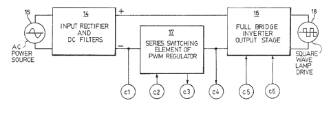
A simplified block diagram of the power circuitry 10
is shown in Figure 3. This comprises essentially an input
rectifier with DC filters denoted by block 14, connected
to an AC power sourca 15, the rectifier feeding a full
bridge inverter 16 via a series switching element 17. The
output of the bridge inverter consists of alternating
square wave current pulses of equal duration for driving
the arc lamp, as denoted by output 18. In Figure 3 the
symbols cl ... c6 denote interconnections with the control
circuits for the power supply, as will be described
subsequently.
Figures 2a and 2b together show the power circuitry
10 in detail. In these figures the block 19, designated
CONTROL/~RIVE, represents the control circuitry 11, 12 and
13 of Figure 1, which will be described in greater detail
hereinafter. Referring to Figures 2a and 2b, the power
circuitry basically comprises a full wave bridge rectifier
21 with smoothing filters 20, energized from the A.C.
power source 15. The rectifier 21 feeds an inverter 22.
The inverter 22 comprises a bridge network of field effect
transistors 23, which are driven by control pulses from
the control/drive unit 19. The output of the inverter 22
is applied to the arc lamp unit 24, which is connected to
the power supply via terminals 25. As shown, the arc lamp
unit 24 comprises a metal halide lamp 26, a high voltage
igniter 27, and additionally includes a conventional door
interlock feature 28 which is interconnected with a supply
circuit 29.
Current from the rectifier 21 is fed to the inverter
22 via a series circuit comprising a switching transistor
30, an inductor 31 and a capacitor 32, the inverter 22
beinq connected in parallel with the capacitor 32 so that
curr~nt supplied by the rectifier 21 to the inverter is
~,
~'
7~2~
6 --
drawn through the switching transistor 30. The rectifier
33 is a free-wheel diode which maintains the flow of
current through the inductor 31. The switching transistor
30, which constitutes the switching element of block 17 in
Figure 3, is itself a field effect transistor and is
controlled by the control/drive unit 19 as hereinafter
described.
Referring now to Figure 5, which shows the block 12
of Figure 1 in greater detail, an 8 MHz master clock
oscillator 40 provides a source of pulses from which
control pulses for the switching transistor 30 and the
bridge inverter 22 are derived. Binary divider circuits
41, which are shown in more detail in Figure 7, are used
to derive from the master clock frequency a sequence of
square wave pulses at a frequency which can be selected
manually by frequency selector 42. In the present example
the divider circuits provide four discrete frequencies 25
kHz, 33.3 kHz, 50 kHz and 100 kH2. The selected sequence
of square wave pulses at the chosen frequency provides a
PWM clock for a digital PWM control pulse generator 43,
and also a control for the bridge inverter 22 via
connection al.
The output from the pulse generator 43, at the PWM
clock frequency, is gated by OR gate 44 with the output
of a comparator 45 which compares a current-responsive
first signal with a voltage-responsive second signal, as
hereinafter described, to derive a difference signal.
This difference signal is applied to the reset input of a
D-type flip-flop 46 and clocked at the PWM clock frequency
to derive the PWM drive for the bridge inverter 22.
Referring now to Figure 4, the PWM clock signal from
the binary divider 41 is applied via connection al (Figure
5) .................................................... O
~2~
-- 7
and connection bl (Figure 4) to binary divider circuits
47, from which four discrete frequencies may be derived.
These frequencies are f/128, f/192, f/256 and f/512, where
f is the PWM clock frequency. The required one of the
four frequencies is selected manually by a frequency
selector unit 48 and applied to a buffer/inverter pair
49, thereby deriving a pair of complementary sequences of
square wave pulses at the selected frequency. The
selected frequency is a submultiple of the PWM clock
frequency. The complementary outputs constitute the drive
for the bridge inverter 22, to which these outputs are
applied via connections b2, b3 (Figure 4) and c5, c6
(Figure 3).
The current responsive signal applied to one input
of the comparator 45, via connection a3 (Figure 5) is a
feedback signal derived from the switching element 17
(Figure 3) via connection c3. As shown in Figure 2a, this
; feedback signal is derived from the currsnt of the
switching transistor 30 by a feedback circuit 50
including a current transformer 51.
The voltage-responsive signal, or voltage reference
signal, applied to the other input of the comparator 45,
via connection a4, is derived from the PWM reference
generator 13 (Figure 1). Specifically, this voltage
corresponds to the voltage applied to the bridge inverter,
which in the present example is nominally 300 volts.
Thus the open circuit, or no load output from the PWM
~ regulator is also 300 volts.
:;
Referring to Figure 6, the voltage applied to
the PWM reference generator via connection d2 will vary
between O and 300 volts, the applied voltage being
inversely proportional to the output voltage of the PWM
regulator 17. This voltage is applied via a potential
,, .
-- 8 --
divider 52, which is designed so that the voltage at
point A will vary in the range 0-5 volts in inverse ratio
to the output voltage of the PWM regulatorO The voltage
at point A is applied to a unity-gain follower 53, which
buffers this voltage from the input resistance of a
unity-gain inverter 54. The output voltage of the
inverter 54, at point B, therefore has a swing of 0-5
volts, being proportional to the output voltage of the
PWM regulator.
The resultant voltage is applied to a dot/bar
National Semiconductor, serving as an analog dot/bar
voltmeter. This device consists of a comparator chain, a
divider network, and a voltage reference circuit, the
driver being used in BAR mode. The device will pull the
outputs 01-010 LOW sequentially as the SIG input varies
~ between the reference voltages R-LO and R-HI.
.~
The reference voltage R-LO, at point E, is set to
correspond to the voltage at point B when the low voltage
end of the specified constant power range is reached at
the PWM regulator output. The reference voltage R-HI, at
point D, is set to correspond to the voltage at point b
when the high voltage end of the constant power range is
reached at the PWM regulator output.
At very low output voltages the feedback comparator
reference to be applied via connections d3 and a4 to the
comparator 45 (Figure 5) is set exclusively by the
potential divider 56. When the minimum normal operating
voltage is reached, i.e. at the low voltage end of the
specified constant power range, the output 01 of device 55
goes LOW, connection R3 in parallel with R2, and reducing
the comparator reference voltage at point C. As the
output voltage increases further, the outputs 02-010 are
24~
switched LOW in sequence, and therefore connect R4, R5 ...
R12 sequentially in parallel with R2. In this way a
constant power characteristic is effectively maintained by
reducing the PWM output current in ten discrete steps as
the output voltage increases through the normal operating
range.
Figura 7 is a simplified diagram of the timing
circuits of Figures 4 and 5. The master oscillator 40 is
crystal controlled, as indicated schematically by the
tuning circuit 60, to provide an output frequency of 8
MHz. The output is applied to a chain of flip-flops 61,
62, 63 forming a frequency divider, to provide a 1 MHz
output. The latter output is applied to the binary
divider circuits 41 constituted by a group of flip-flops
64, 65, 66, 67 interconnected so as to derive four
possible frequencies 25 kHz, 33.3 kHz, 50 kHz and 100 kHz.
A multiplexer 68, controlled by manually operable selector
switches 69, is used to select one of those frequencies
thereby providiny a sequence of square wave pulses at the
first reference frequency previously referred to, (i.e.
the PWM clock). The PWM clock is applied to the digital
PWM control pulse generator 43, the output of which is
processed as previously described to control the switching
transistor 30.
The PWM clock is also applied to the further
frequency divider circuits 47 comprising a binary divider
;~ 70, a chain of flip-flops 71, 72t 73, and a multiplexer
74. The arrangement provides four possible frequencies,
each of which is a submultiple of the first reference
frequency, and the required frequency is selected by
manually operable switches 75 to provide a sequence of
square wave pulses to be fed to the buffer/inverter pair
49 as previously described.
. , .
~7~Z~
- 10 -
SUPPLEMENTARY DISCLOSURE
A second embodiment of the invention will now be
described with reference to Figures 8, 9 and 10 of the
accompanying drawings, in which:
Figure 8 is a schematic block diagram of the master
clock and PWM generator, corresponding to the block 12 in
Figure 1, in a second embodiment of the invention;
Figure 9 is a wiring diagram of khe PWM reference
generator, corresponding to the block 13 in Figure 1, in
the second embodiment of the invention; and
Figure 10 is a waveform diagram to be read in
conjunction with Figure 9.
In the power supply arrangement described above with
reference to Figures 1 to 7, a constant power output
characteristic is obtained by using a direct voltage
feedback means to control the output current threshold.
However, in this alternative arrangement the PWM reference
generator and its associated circuitry are modified to
provide a constant power output characteristic which is
even simpler, more stable, and more precisely controllable
than that described above.
~;
It is common practice in many current-mode voltage
regulator circuits to use an arti~icial ramp voltage to
provide slope compensation. The ramp voltage is either
summed positively with the current feedback signal, or
summed negatively with a reference voltage. The usual
purpose is to add a second pole to the loop response of the
~eedback circuit, which makes the PWM stable with duty
~actors greater than 0.5. It also keeps the average
inductor current proportional to the peak inductor current
over a wide range of duty cycles. The principle also
J
z~ ~
applies to fixed frequency PWM voltage regulators designed
to drive resistive loads. Thus, in a power supply
according to the present invention it has been found that,
by applying over-compensation by means of summing the
artificial ramp with the current feedback signal, one
cannot only achieve tha benefits listed above Eor duty
cycles in excess of 50%, but can also obtain a constant
power output characteristic.
Figure 8 shows the master clock and PWM generator of
this second embodiment of the invention. The diagram
corresponds closely to that of Figure 5 and corresponding
components are denoted by the same reference numerals as
are used in Figure 5. However, in this case the reference
source for the comparator 45 is a fixed voltage source
derived from a potential divider Rl and R2. The current
feedback signal (a3) is derived from the circuit shown in
Figure 9, which comprises essentially an artificial ramp
generator 90, a voltage follower 91, and a summing network
92. The artificial ramp generator 90 comprises an RC
network, shown as a resistance 93 or capacitance 94, with
a FET 80 connected across the capacitance. The FET 80
rapidly discharges the capacitance 94 on each reset pulse
(dl) from the PWM control pulse generator 43 (Figure 8~.
The output of the ramp generator 90 is buffered by
an operational amplifier 81 constituting the voltage
follower 91, the buffered output being summed with a
current feedback signal (d2) from the series switching
element 17 of the PWM regulator (Figure 4). The output of
the summing network 92 (d4) defines the current feedback
signal (a3) to be applied to the non-inverting input of
the comparator 45.
The waveforms representing the reset pulse (dl) and
the buffered output of the operational amplifier 81 (d5)
are shown in Figure 10. It will be seen that the
- 12 ~
instantaneous voltage of the ramp waveform increases as
the PWM ON-time, and hence the output voltage, increases,
and so less current is required to reset the PWM as the
voltage increases. Clearly, with such an arrangement, the
values of the summing resistors 95, 96 of the summing
network 92 can be selected to provide about a near perfect
stepless constant power output characteristic over a wide
range of operating voltages.
,,~ .
.~