Note: Descriptions are shown in the official language in which they were submitted.
~;~780S~
P-87,1969
S87P2~9
FILTER ADJUSTMENT APPARATUS AND M~TEIOD
BACKGR~UND OF THE INVENTION
Field of the Invention
This invention relates to a filter adjustment apparatus and
m0thod and more particularly to a device and method for adjusting
a filter connected in series with a signal processing circuit or
a filter connected in series with at least one other ~ilter.
Description of the Prior Art
In a checking process for electronic circuits in general, it
may become necessary to adjust the paak frequency, dip fraquency
or the cut-off freq~1ency of the filter circuit to a prescribed
target value. Above all, in a circuit formed in an analog
intsgrated circuit or analog IC, while the circuit elements such
as transistors, resistors or capacitors can be fabricated with a
highly accurate relative ratio of the rated values thereof, the
absolute values or magnitudes of these rated values vary from
circuit to circuit. Hence, the aforementioned adjustment is
thought to be indispensable in a filter circuit wherein a demand
is raised for high accuracy.
In general, when carrying out the filter adjustment, the
filter output is detected while tha frequency of the input
signals to the filter is continuously changed, by so-called
sweeping, for finding the portions proper to the filter
characteristics, such as the peak or dip on the frequency
characteristic curve, and the frequency characteristics are
changed until the frequency thereof coincides with the prescribed
target values.
8~
It is noted that~ when adjusting the cut-off, peak
or dip frequencies o~ a filter connected in series with
one or more other filters or a ~ilter connected in series
with a signal processing circuit, the frequency
characteristics of the series circuit including the
filter will appear as the combined characteristics of the
respective filters or as the combined characteristics of
the filter and the signal processing circuit, so that it
becomes difficult to check for portions proper to the
~ilter characteristics, such as the aforementioned peak,
dip or cut-off points. Above all, when the series filter
circuit is provided in an integrated circuit, it is
almost impossible to input or output signals into or from
the respective filters or the signal processing circuit.
In addition, since the adjustment of the respective
filters is per~ormed simultaneously by the common
adjustmant control signal, such that the frequency
characteristics of the respective filters are changed
simultaneously, the combined frequency characteristic~
are changed in a complicated way, so that it becomes more
difficult to locate the portions proper to the filter
characteristics, such as the aforementioned p~ak points.
With increased difficulties in locating the
charac~eristic portions, filter adjus~ment accuracy is
undesirably lowered, while the labor and the time
-2-
~2~
involved in the adjustment ara increased.
Obiect and Summary of tbe Invention
It is there~ore an object of the present invention
to provide a filter adjustment apparatus and method
whereby the characteristic portions such as the peaks,
dips or cut~ofP points on the filter frequency
characteristic curve may be located by a simplified
structure with increased adjustment accuracy and
shortened adjustment time.
The ~ilter adjustment apparatus and method according
to the present invention is characterized in that it
comprises a filter, the characteristics of which are
adjusted in dependence upon the adjustment data, a signal
processing circuit connected in series with said filter,
and means ~or setting said signal processing circuit to a
state not influencing said filter characteristics during
the time of filter adjustment.
Said means may include causing said signal
processing circuit to be by-passed so as not to affect
the filter characteristics. The signal proc ssing
circuit includes other filters, emphasis circuits,
modulator/demodulators or level control circuits.
BRIEF DESCRIPTION OF THE DRAWINGS
Fig. 1 is a block circuit diagram showing a filter
adjustment apparatus according to an embodiment of the
,: -3-
Q~'`
a~5~
present invention.
Fig. 2 is a chart showing the frequency
characteristics for explaining the operation o~ Fig. 1.
Fig. 3 is a chart showing the frequency
characteristics for the trap filter.
Fig. 4 is a ¢hart showing an example of the
adjustment operation of the trap filter.
Fig. 5 is a block circuit showing an example of the
biquad filter.
Fig. 6 is a circuit diagram showing a practical
example of an integrator employed in the filter of Fig.
5.
Fig~. 7A, B and C are charts showing frequency
;~ characteristics of a series circuit of an LPF and a BPF.
Fig. 8 is a block circuit diagram showing an example
of constituting a BPF by a biquad filter.
Figs. 9A, B and C are charts showing frequency
characteristics f~r explaining the frequency
characteristics of a series circuit consisting of two
trap type ~ilters.
: -3a-
.
11273~ 5~
Fig. 10 is a block circuit diagram sho~ing essential parts of
an embodiment using a series circuit consisting of a signal
processing circuit and a filter.
Fig. 11 is a block circuit diagram showing a practical
example of an analog IC to which the present invention is
applied.
Fig. 12 is a block circuit diagram showing a filter
adjustment device accordlng to a modified embodiment of the
present invention.
Fig. 13A, B and C are charts showing frequency
characteristics for explaining the operation thereof.
Figs. 14 to 17 are circuit diagrams showing practical
exemplary circuits for commutation of filter aharacteristics.
Figs. 18 to 20 are charts showing frequency characteristics
for explaining the main operation of modified embodiments.
Fig. 21 is a circuit diagra~ showing essential parts of the
embodiment shown in Fig. 20.
Fig. 22 is a block circuit diagram showing a further modified
embodiment of the prese~t invention.
DESCRIPTION OF THE PREFERRED EMBODIMENTS
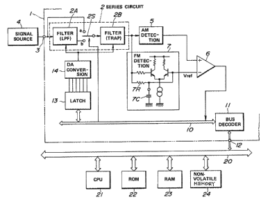
Fig. 1 is a block diagram showing a filter adjustment
apparatus according to a prefarred embodiment of the present
invention. In the present embodiment, the apparatus includes an
analog integrated circuit 1, such as an IC for sound multiplex
demodulation used for example ~n a television receiver. The IC
includes a series circuit including a filter to be adjusted by
tha present device, for example a series circuit 2 mainly
composed of a first filter 2A as the signal processing circuit
and a second filter 2B to be adjusted by the present filter
adjustment apparatus.
--4--
~L2~ S~
Rsferring to Fig. 1, signals from a signal source 4, such as
sinusoiclal waves, are supplied to the series circuit 2 through an
exterior connection terminal 3, such as a so-called IC pin, of
the analog integrated circuit 1. To -the filters 2A and 2~ within
the circuit 2, common filter adjustment data are supplied through
a RAM 23, an external bus line 20, a bus decodes 11, an internal
bus line 10, a latch 13 and a D/A converter 14 for changing their
respective circuit constants, such as the current values of the
constant current sDurces, for changing the filter
characteristics. A bypass line is connected parallel to the
filter 2A, or a signal processing circuit in general, and a
changeover switch 2S, adapted for selective commutation between
the filter 2A and the bypass circuit, is connected between the
filter 2A and the next stage filter 2B. The switch 2S is
commutated by a commutation signal supplied from a ROM 22 through
an external line 20 and the internal bus line 20 within the IC.
The input signal from the external connaction terminal 3 is fed
to a select terminal a of the changeover switch 2S through the
bypass line, while the output from the filter 2A as the signal
processing circuit is supplied to a select terminal b of the
changeover switch 2S.
In the present embodiment, the filters 2A and 2B are assumed
to have low pass filter aharacteristics as shown in Fig. 2A and
what is called the trap characteristics as shown in Fig. 2B,
respectively, as typical of the filter frequency
characteristics. Fig. 2C shows the combined characteristics of
the two filter characteristics. During filter adjustment, the
changeover switch 2S is leveled to the side of the terminal b to
by-pass the filter 2A such that the trap characteristics of the
filter 2B will appear directly as the output characteristics of
the series circuit 2, as indiaated by a broken line in Fig. 2C.
Since the dip frequency of the trap characteristics can be read
--5--
~78~S~
easily and accurately, the dip fre~uency can be ultimately
adjusted to the presecribed target fre~uency fO b~ way of
performing the filter adjustment.
Filter adjustment in accordance with the output from the
series circuit 2 can be made in various ways. According to the
present embodiment, filter adjustment is performed in such a
manner that the output from the series circuit 2 is supplied to,
for example, an AM detector 5 as the level detacting means for
detecting the signal level or amplitude, the so-detected AM
output being supplied to one terminal, such as a non-inverting
input terminal, of a comparator 6 for signal level
discrimination. A prescribed reference level Vref is supplied to
the other input terminal or an inverting input terminal of the
comparator 6. In the comparator, it is determined whether the
level of the detected AM output is higher or lower than the
reference level Vref. According to the present embodiment, the
reference level Vref is obtained from the low pass filter portion
of the FM detector 7 provided in the analog IC 1. To this FM
detector 7 is supplied the output from the series aircuit 2, the
direct current component of which is taken out by a low pass
filter or LPF which is usually provided in an input stage side
limiter amplifier of the FM detector. This low pass filter
comprises an RC circuit composed of an input resistance 7R and a
capacitor 7C, and the direct current signal is supplied as the
reference level Vref to the comparator 6 through this low pass
filter.
The output of comparison or the level discrimination output
from the comparator 6 i~ supplied to the internal bus 10 within
the IC 1. The bus decoder 11 connected to the internal bus 10 of
the IC is also connected through a bus for external connection 12
to an external bus 20 and used as an interfacing circuit for
mutual conversion of the data on the external bus 20 and those on
--6--
~27~DSi~
the internal bus 10. The data transmitted from the
external bus 20 through the bus decoder ll to the
internal bus 10 are stored once in a latch circuit 13 and
then conYerted into analog signals in a D/A converter 14,
the resulting analog signals being supplied to the
respective filters 2A and 2B in the series circuit 2 as
the circuit constant control signals or as the filter
characteristic adjustment signals. To the external bus
are connected a CPV 21, such as a so-called
microprocessor, the ROM 22 storing various programs and
data, the RAM 23 ~or transient data storage and a non-
volatile memory 24 ~or storage of data, such as the
filter adjustment data, irrespective of the turning on or
of~ of the power source. The computer system composed of
the CPU 21, ROM 22, RAM 23 and the non-volatile memory 24
performs a series of control operations including storing
the filter adjustment data depending on the outputs
obtained from the comparator means when the filter
adjustment data are changed, and determining the optimum
filter adjustment data on the basis of the thus store~
filter adjustment data.
The filter adjustment for finding the aforementioned
filter adjustment data is now explained.
In making the filter adjustment in general, the
7-
,~.,
:
aforementioned dip frequency may be detected on the basis
of the filter output characteristic curve or the
frequency response curve that is obtained when changing
or sweeping the input signal frequency, with the
frequency sweeping being repeated until the dip frequency
is equal to the target frequency fO while adjusting the
filter characteristics, as conventionally. There is
however proposed in the present embodiment a system as
shown in Fig. 1 wherein filter adjustment can be made
automatically and precisely by a circuit of a simpler
structure.
Briefly, the filter adjustment system is so designed
that the optimum filter adjustment data are found on the
basis of the
-7a-
,~
filter ad~ustment data corresponding to the crossing of a
prescribed re~erence level by the level detection ~ilter output
for changes caused in the filter characteristics with respect to
the input signals fixed at the constant frequency fO.
For filter adjustment, the changeover switch 2S is leveled to
the terminal _ so that only the trap characteristics of the
filter 2B as shown in Fig. 3 will be manifested as the
characteristics of the circult ~-. The filter characteristics are
then adiusted so that the dip fre~uency of the trap
characteristics will be equal to the prescribed target frequency
fO. To the series circuit 2 are supplied signals at the constant
frequency fO from the signal source 4. At this time~ control
means composed of the computer system including the CPU 2i
transmit filter adjustment data to the control terminals of a
constant current source I2 of each of the filters 2A and 2B of
the filter circuit 2. These adjustment data represent a series
of data for gradually shifting the characteristic curves of the
filter ~B in one direction, for example, in the arrow mark
directi~n as schematically indicated by the dotted lines in the
figure, on the frequency axis. It is noted that changing the
frequenc~ characteristics substantially continuously is
tantamount to changing or sweeping the input signal frequency.
Conversely, since the input signal frequency is fixed at the
constant value fO, the output obtained after level detection of
the output signals from the filter 2 at the AM detector 5 is as
shown for exampla at the detected output in Fig. 4. The detected
output has its level changed in accordance with the changes in
the filter adjus-tment data as indicated on the abscissa in Fig.
4. Thus, the curve of the detected output corresponds to the
filter characteristic curve of Fig. 3 when supposed that the
curve is inverted in the left and right direction in Fig. 3 with
the frequency fO as the center. This detected output is supplied
--8--
~L2~ 4
to the non-inverting input terminal of the comparator 6
for comparison with the reference level Vref to produce
the comparator output as shown in Fig. 4. The filter
adjustment data is obtained at the inverting position of
the comparator output, that is, when the detected output
crosses the reference level Vref, and are sequentially
denoted as Da and Db. The optimum adjustment data, when
the dip ~requency of the trap characteristics coincides
with the aforementioned frequency fO, is obtained from
the mean value of the data Da and Db or (Da + Db)/2.
This optimum adjustment data are written in the non-
volatile memory 24 o~ Fig. 1 and preserved even when the
power source is turned off. As one of the usual
initializing operations performed at the time the power
source is turned on, the aforementioned optimum
adjustment data stored in the non-volatile memory 24 are
transmitted to the latch circuit 13 through the buses 20
and 10 for establishing the optimum adjustment state of
the filters 2A and 2B in the filter circuit 2.
It is possible with the above arrangement to
eliminate the conventional frequency sweeping, while
simplifying the circuit structure and shortening the time
otherwise necessary for adjustment. In addition, it is
possible to obtain the optimum filter adjustment data
with high accuracy by a simpler circuit ctructure adapted
_g_
' ~
3L2713~54
for detecting the crossi.ng point of the references level
by the filter output, with the monitoring of the
characteristic curve being also eliminated, while the
circuit can be easily adapted to automatic adjustment
with the use of the buses.
It is noted that, as the filters 2A and 2B
incorporated into the integrated circuit, the so-called
biquad filter as shown, for example, in Fig. 5, is most
popular. The biquad filter is an active filter
consi~ting of a series connection ~f a first
-9a-
.
.
:~2'7~5~
integrator composed of an operational amplifier 31 and an
inegrating capacitor 32 and a second integrator composed of an
operational amplifier 33 and a capacitor 34. The output of the
operational amplifier 31 is supplied to the non-inverting input
terminal of the operational amplifier 33 while the output of the
operational amplifier 33 is fed back to the inverting input
terminal o the operational amplifier 33 and the output of the
operational amplifier 33 is fed back to the inverting input
terminal of the operational amplifier 33 through a feedback
circuit 35 having a feedback factor equal to ~.
It is noted that the characteristics of BPF, LPF, HPF, trap
or phase shifters can be realized by suitably selecting whether
input signals should be supplied to the non-inverting input
terminal of the operational amplifier 31 or to capacitors 32, 34,
or the terminal or capacitors should be grounded.
In the embodiment shown in Fig. 5, input signals are supplied
through the terminal 36 to the non-inverting input terminal of
the operational amplifier 31 and to the capacitor 34 while the
capacitor 32 is grounded and the output signals are taken at an
output terminal of the operational amplifier 33 to provide a trap
filter. The frequency characteristics of the trap filter are
repres~nted by a transfer function
S2 + ~s + 1
wherein s=; -, ~0= 2~fo,~ =2~f and fO reprssents the trap
frequency.
Also the input signals can be supplied only to the
non-inverting input terminals of the operational amplifier 31,
while both the capacitors 32, 34 can be grounded and the output
signals taken out at the operational amplifier 33 to provide an
LPF. The transfer function of the ~PF iS given by
--10--
~5~
S2 + ~S ~ 1
where S=~ 0= 2~fo, ~= 2~f and fo is the cut-off frequency of
the low pass filter.
Fig. 6 shows an example of an integrator used in the above
biguad filter. Referring to Fig. 6, the non-inverting input
terminal 41 and the inverting input terminal 42 of the
operational ampli ier are connected to the base terminals of
transistors 43, 44 cojointly forming a differential amplifier.
The current flows in a resistor RE connected between the emitters
of these transistors 43, 44 with a magnitude related to the input
voltage between the terminals 41 and 42. The current equal to
the sum of the current I~ of the constant current sources
connected to the emitters of the transistors 43, 44 and the
current e~ual to the difference between the currents Il,Il flow
respectively through diodes 45 and 46 connected to the collectors
of the transistors 43, 44 respectively. The terminal voltages of
these diodes 45, 46 appearing as a function of these currents are
applied to the base electrodes of transistors 47, 48 cojointly
forming an emitter common differential transistor pair. The
common emitter of these transistors 47, 48 is grounded via a
constant current source 49 of the current 2I2, such that the
signal current flowing at the collactor side of the differential
transistor pair is amplified by a factor of I2/Il. The collector
output of the transistor 4a is taken through a current mirror
circuit 50 composed of a diode 50a and a transistor 50b for
charging the capacitor 52 used as the aforementioned integration
capacitance. The voltage at one end of the capacitor 52 is
inputted to a transistor 54 so as to be taken at an output
terminal 55. The other side 53 of the capacitor 52 may be
grounded, as described above, an input signal is supplied
thereto.
~2'?~5~
In the configuartion of the integrating circuit shown in Fig.
6, changes in the current I2 of the current source 51 on the
output side of the current mirror circuit 50 and the constant
current source ~9 result in a parallel displacement of the
characteristic curves along the fre~uency axis, as explained by
reference to Fig. 3. This phenomenon is utili~ed for filter
adjustment, as already described above.
It is noted that a variety of configurations can be envisaged
for the consititution of the filters 2A and 2B making up the
series circuit 2.
For example, when the LPF (i.e. the low pass filter) having
the frequency characteristics shown in Fig. 7A is used as the
first filter ~A and the BPF (i.e. the bandpass filter) having the
characteristics shown in Fig. 7B is used as the second filter 2B,
the combined filter characteristics are as shown by the solid
line in Fig. 7c, such that it becomes difficult to check for the
peak frequency fO. Therefore, during the time of the filter
adjustment mode, the first filter 2~ is by-passed as in the above
described embodiment so that the BPF characteristics of the
second filter 2B are directly manifested as the characteristics
of the circuit 2, as indicated by the dotted line in Fig. 2c.
Fig. 8 illustrates an example of the aforementioned biguad
filter for the realization of the bandpass filter. In this
figure, parts or components same as those of Fig. 5 are indicated
by the same numerals and the corresponding description is
omitted. A feedback circuit 35 is composed of a voltage dividing
circuit composed of resistors Rl and R2, with the resistor R2
being connected to an output terminal of an operatinal amplifier
33 and the voltage output divided by the resitors R1 and R2 being
fed back to an inverting input terminal of the operational
amplifier 33. Both the non-inverting input terminal o~ the
operational amplifier 31 and the capacitor 34 are grounded and
-12-
~L~'7~S~
-the input signal is supplisd through a terminal 36 t~ the
capacitor 32 and the resistor R1 to provide the BPF.
Figs~ 9A, 9B and 9C illustrats the characteristics of the
filters 2A and 2B and the combin2d characteristics of the series
circuit 2 for the case in which the filters 2A and 2B have trap
characteristics of different dip frequencies fo2 and f~1. The
arrangement is so made that the filter 2A is by-pass2d as
describea above so that the dip portion of the characteristics of
the filter 2B i5 manifested substantially directly as the
combined characteristics of the series circuit 2, as indicated by
the dotted line in Fig. 9C.
It is also possible to envisage various other combinations,
such as using BPFs or the BPF and the trap filter as the two
filters.
The present invention may also be applied to a series circuit
2 composed of a filter 2F and a signal processing circuit 29 in
general, such as tha AM or FM modulators or demodulators, level
controllers, equalizers or emphasis circuits. Similarly to the
preceding embodiment, a by-pass line is provided parallel to the
signal processing circuit 2 and a changeover switch 2S is
provided for commutation between the circuit 2P and the filter
2F. During the filter adjustment, the changeover switch 2S is
commutated to by-pass the siynal processing circuit 2P so that
the characteristics of the filter 2F will be displayed
unambiguously. Tha aforementioned filter adjustment signals are
supplied to the filtar 2F through the adjustment control terminal
2K. The circuit may be configured otherwise in the same way as
in Fig. 1.
The substantial parts of the integrated circuit (IC) for
sound multiplex demodulation as a practical example of the analog
IC for application of such automatic filter adjustment, are
explained briefly by referring to Fig. 11.
-13-
~s~
In this figure, an input terminal 61 is used as a signalinput terminal of an integrated circuit (IC) for sound multiple~
demodulation. Thus, the sound multiplex signals ob~ained upon
reception of the television sound multiplex broadcasting, for
example, are supplied to the terminal 61. The ~ound multiplex
signals supplied to the terminal 61 are amplified by a voltage
controlled amplifier VCA) 50 as to be then supplied to a main
signal system, a sub signal system and to a control signal
system. The sub signal system has a BPF circuit composed of a
BPF 63, a trap filter 64 and a BPF 65 and manifesting bandpass
characteristics in its entirety, and an FM detector 66, and is so
designed as to take out the output from the FM detector 66 as the
sub voice through an LPF circuit and a de-emphasis circuit, not
shown. The control signal system is composed of a BPF 68 to
which is supplied an output from an amplifier 67 connected
between the ~PF 63 and the trap filter 64, a filter 69
manifesting bandpass (BP) and trap characteristics, an AM
detector 71 to which is supplied an output from the filter 69
through an amplifier 70, and an FM detector 72 to which is
supplied an output from the AM dectector 71. For more reliable
detection of the sound multiplex mode, the output appearing in
the vicinity of the output stage of the limiting amplifier of the
FM detector 66 of the sub signal system is supplied to an AM
detector for level deteGtion and thence to a comparator circuit
74 ~or determining the presence or absence of the sound multiplex
subcarrier. The output from the comparator 74 is supplied to an
operation inhibit or defeat terminal of the FM detector 72 of the
control signal s~stem for controlling the FM detector 72 to an
inoperative state in case the sound multiplex subcarrier is not
detected.
In the circuit of Fig. 11, D/A converters 75, 76 are
provided, as characteristic of the present embodiment. The
-14-
~:7~3~5~
function of the DfA converter 75 is to control themagnitude of the current of the aforementioned constant
current source to thereby control the frequency
characteristics of the FM detector 66 and the filters 63,
64 and 65 of the sub signal system, whereas that of the
D/A converter is to control the frequency characteristics
of the filters 68 and 69 of the control signal system.
Changeover switches 77, 7~ and 73 are connected between
the FM detector 66 and the BPF 66 of the sub signal
system, between the trap filter 64 and the ~M detector 73
and between the BP and the trap filter 69 and the BPF 68
of the control signal system, respectively, with a
movable contact being shifted to the select terminals a
and b for usual sound multiplex signal demodulation and
for filter adjustment, respectively. That is, during the
mode of demodulation of the sound multiplex signals, the
changeover switches 77, 78 and 79 are commutated to the
side of the select terminal a, the output from the BPF 65
is supplied to the FM detector 66, the output of the
limiting amplifier of the FM detector 66 is supplied to
the AM detector 73 and the output from the BPF 68 is
supplied to the BP and trap filter 69. During the mode
of filter adjustment, as described hereinabove, the
output from the trap filter 64 is amplified by an
-15-
~,
~ 3Q5i4
amplifier-changeover switch 78 so as to be then supplied
to the AM detector 73 and the changeover switch 77, while
the output from the changeover switch 77 is supplied to
the FM detector 66 and the output from the amplifier 67
is directly ~upplied to the BP and trap filter 69 of the
control signal system. During this filter adjustment~
the BPF 55 ~f the sub signal system is by-passed while
the output from the trap filter 64 is level-detected in
an AM detector 73 corresponding to the AM detector 5 of
Fig. 1 and transmitted to a comparator 6 where it i5
compared to the direct current level Vref from the RC
circuit of the FM detector 66 corresponding to the FM
detector 7 of Fig. 1. In the control signal system, the
BPF 68 is by-passed so that the characteristics of the
BP and trap filter 69 may be displayed more definitely.
Fig. 12 shows in a block circuit diagram a filter
adjustment device according to another embodiment of the
present invention. The parts or components equivalent to
those shown in Fig. 1 are depicted by the same reference
numeral~.
Referring more specifically to Fig. 23, a sinusoidal
wave signal, for example, from the signal source 4 is
supplied through a terminal for external connection of an
analog IC, or a so-called IC pin, to the ~ilter circuit 2
-16-
~`
.
to be adjusted in accordance with the present invention.
The two filters 2A and 2B of the ~ilter circuit 2 are so
designad that the circuit constants thereof, such as the
current magnitudes of the constant current source, are
changed with the common filter adjustment data supplied
~rom the D/A conv~rter 14 as later described for
changing the filter characteristics. At least one of the
filters, for example, the filter 2B, can be commutated
for drastically changing the filter characteristics. The
frequency characteristics of the filter 2B when
commutated in this manner are designed to reduce the
effect on the characteristic portions of the frequency
characteristics of the other filter 2A, such as peaks,
dip or cut-off points. In the present embodiment, the
filters 2A and 2B o~ the filter circuit 2 are presumed to
have the so-called trap characteristics as shown in
Fig. 13A and the LPF characteristics as shown in
Fig. 13B, respectively. The combined characteristics are
as shown in Fig. 13C. By commutating the characteristics
of the filter 2B as described hereinabove, the cut-off
frequency of the LPF characteristics are shifted towards
the higher frequency as indicated by dotted line in
Fig. 13B so that the dip portion of the trap
characteristics of the filter 2A i5 completely includPd
within the passband of
-16a-
the LPF characteristics. The comhined characteristics of the
filt0r circuit 2 thus commutated are such that, as indicated by a
broken line in Fig. 13C, the dip portion of the trap
characteristics of the filter 2A is manifested more definitely so
that the dip freq~ency can be read more easily and precisely and
hence the filter adjustment can be made more easily and with high
precision when ultimately adjusting the dip frequency to the
preseleGted frequency fO.
The operation of the present embodiment is otherwise the same
as in Fig. 1 so that the detailed description is not made herein
for simplicity.
Referring now to the commutation of the characteristics of
th~ filter 2B having, for e~ample, the LPF characteristics as
described above, it is made by commutating the internal circuits
of the filter as by a switch in such a fashion that the filter
characteristics are vitally changed from those having a cut-off
freguency fl, as indicated by the solid line ln Fig. 13B, to
those having a cut-off frequency f2, as indicated by the dotted
line therain. In the integrating circuit shown in Fig. 6,
commutation of the filter characteristics can be achieved by
commutating the capacitance C of the capacitor 52 or integration
capacitance, commutatiny emitter resistance RE of the input stage
to modify the mutual conductance gm or by commutating the I1/I2
ratio equivalent to the gain of the operational amplifier.
Fig. 14 shows a typical circuit for commutating the
integration capacitance. Referring to this figure, a series
circuit consisting of a switch 52SW and a capacitor 52C2 is
connected in parallel with the capacitor 52 of the integrated
circuit of Fig. 6 and the switch 52sw is turned off or on
according as the filter adjustment is or is not performed,
respectively, for thereby commutating and changing the LPF
characteristics. With capacitances C1 and C2 of the capacitors
-17-
~278~S~a
52 and 52C2, the swl~ch 42SW is turned on during the ~ormaloperation, with the filter adjustment not being made, and the
cut-off frequency fCl of the LPF characteristics is given by
C1 I2
2~(C1 ~ C2)REI1
During the time of filter adjustment, the switch 52SW is turned
off and the cut-off frequency fC2 g
C2 2~ClREIl
while commutation is made to LPF characteristics as indicted by
the dotted line in Fig. 13B.
In the typical circuit shown in Fig. 15, a series circuit
consisting of a switch SWRE and a resistor REE is connected in
parallel with an emitter resistance RE of the input stage of the
integrator. The switch SWRE is turned off and on for normal
operation and for filter adjustment, respectively, for
commutating the mutual conductance. During the normal operation
with the switch SWRE being turned off, the cut-off freguency fC
is given by
:ECl 21rCREIl
and, during tha filter adjustment, the switch SWRE being turned
on, the cutt-off freguency fC2 ~s given by
C2 I2
2~C(RE//REE)I1
where R //R = E EE
In the examples of Figs. 16 and 17, the current ratio I2/
is commutated to change the above gain. First, in the circuit
shown in Fig. 16, a series circit consiting of a switch 49SW and
a constant current source 4913 f a current magnitude I3 is
connected in parallel with the constant current source 49, while
-18-
~27~as~ .
a series circuit consisting of a switch 51SW and a constant
current source 51l3 of a current magnitude I3 is connected in
parallel with th0 constant current source 51. The switches ~9SW
and 51SW are interlocked so that they are simultaneously turned
off during the normal operation and simultaneously turned on
during the filter adjustment. The constant current sources ~9,
51 are usually configured as the current mirror circuits.
Referring to ~ig. 17, a series circuit consisting of a switch 58
and a constant current source 59 of a current magnitude I3 is
connected in parallel with a constant current source 57 of the
current magnitude I2 connected to an input sids transistor 56
constituting a current mirror circuit along with transistors 49,
51 of respective constant current sources, with the switch 58
being adapted to be turned on and off during standby and during
the filter adjustment, respectively. The cut-off frequency fC
for standby is given by
C1 2
2 7rCREI 1
while ths cut-off frequency fC2 for filter adjustment with the
switch SWRE turned off is given by
I2 + I3
C2 2~CREI1
The above described commutation of the internal circuit of
the integrator may be performed for one or both of the two
integrators constituting tha aforementioned biquad filter.
It is to be noted that the fre~uency shifting by the
commutation of the internal circuits may be achieved not only in
the case of the LPF but in various other filters, such as BPF,
HPF or trap filters, and that the circuit may be easily adapted
to automatic adjustment with the use of the buses.
It is also possible to envisage various combinations of the
filter characteristics of the filters 2A and 2B constituting the
filter circuit 2 of Fig. 12.
--19--
For example, when using the bandpass filter having
the frequency characteristics ~hown in Fig. 18A as the
first filter 2A and using the lowpass filter having the
frequency characteristics shown by the solid line in
Fig. 18B as the second filter 2B, the combined filter
characteristics ara as shown by the solid line in
Fig. 18C, such that it becomes difficult to ascertain the
peak frequency fO. Therefore, during the mode of the
filter adjustment, the characteristics of the second
filter 2B are commutated similarly to the preceding
embodiment for shifting the cut-off frequency drastically
towards the high frequenry side, as shown by the broken
line in Fig. 18B, such that the characteristics of the
first filter 2A are display d substantially directly as
the characteristics of the filter circuit 2, as indicated
by the broken line in Fig. 18C.
Figs. 19A, B and C illustrate the characteristics of
the ~ilters 2A and 2B of the ~ilter circuit 2 having trap
characteristics and the dip frequencies fOl~ fo2,
respectively, and the combined characteristics of these
filters. The characteristics of the filter 2B are
commutated for shifting the dip towards, for example, the
hlgh frequency side, as shown by the broken line in
Fig. l9B, whereby the dip portion proper to the
20-
~.
i4
characteristics of the filter 2A are displayed
substantially directly as the combined characteristics of
the filter circuit 2, as indicated by the broken line in
Fig. l9C.
When both of the two filtars are bandpass filters or
at least one of the filters is the combination of the BPF
and the trap filter, it is also possible to reduce the
value of Q (quality factor) of the BPF and to commutate
the acute peak curve shown by the solid line in Fig. 20
to a more gentle curve shown by the broken line therein
to render the characteristic curve of the other filter
more explicit.
Fig. 21 illustrates a typical circuit for
commutating the Q of the BPF.
In this figure, parts or components equivalent to
those of the biquad filter shown in Fig. 3 are indicated
by th~ ~ame reference numerals and the corresponding
description is omitted for simplicity. A feedback
circuit 35 is constituted by a voltage divider consisting
of resistors 35Rl and 35R2~ with the resistor 35R2 being
connected to an output terminal of an operational
amplifier 33 and with the divided voltage output of the
resistors 35R1~ 35R2 being fed back to the inverting
input terminal of the operational amplifier 33. As the
-21-
~`'
:
~,
~LZ~ 54
means for changing the commutating the Q, a series
circuit consisting of a resistor 35R3 and a switch 35SW
is connected in parallel with the resistor 35Rl The
feedback factor of the feedback circuit 35 is commutated
in dependence upon the turning on and off of the switch
35SW for commutating the value of Q or 1/~ . Thus, with
the resistances of the resistors 35R1~ 35~2 and 35R3 f
R1, ~2 and R3, respectively, the value f QOFF for the
switch 35SW being turned off and that f QON for the
switch 35SW being turned on are given by
~ 2
QOFF ~
and ~ R1/ /R3 ) ~R2
QONRl//RR
;
R1 ~3
wherein R1//R3 ~ ~ R3 Since QON>QOFF~ ~he switch
35SW is turned on during the standby time to realize.the
PFF having the prescribed high Q and turned off during
the filter adjustment to lower the value of Q as
indicated by the broken line in Fig. 20 to increase the
curvature of the characteristic curve to thereby
demonstrate the characteristic portion proper to the
other filter to facilitate the filter adjustment.
-2la-
`'.~'
i,4
Fig. 22 illustrates a further modifided embodiment of the
present invention wherein D~ converters l~A, 14B and latch
circuits 13A, 13B are separately provided to each of the filters
2A and 2B of the filter circuit 2. The circuit shown in Fi~. 22
is otherwise the same as that shown in Fig. 1 so that the
correspondin~ parts are indicated by the same reference numerals
and the corrssponding desoription is omitted for simplicity.
In the present modified embodiment, the filter adjustment
data of the respective filters 2A and 2B can be adjusted
separately, a pred~termined offset may be annexed to the filter
adjustment data of one of the filter 2B for realizing the
aforementioned changing or commutation of the filter
characteristics. After termination of the filter adjustment, the
obtained optimum adjustment data may be used as the data for the
filters 2A and 2B in consideration of the high relative accuracy
of the components of the same integrated circuit.
The present invention is not limited to the above described
specific embodiments, but may comprise various other
modifications. For example, the present invention may be easily
adapted to a series circuit including three or more filters. It
is also possible to change or modify various filter
characteristics drastically including shifting the cut-off
frequency of the highpass filter towards the low frequency side
for thereby demonstrating the portion charactsristic of the other
filter more explicitly.