Note: Descriptions are shown in the official language in which they were submitted.
-1- 25307-187
BACKGROUND OF THE INVENTION
The present invention relates to a supervisory system
for a primary group digital transmission line system, such as
a PCM-30 channel or PCM-24 channel sys-tem.
ReEerence will now be made to the accompanying
drawings, in which:
FIGURE 1 is a block diayram of a primary group trans-
m.ission line system;
FIGURE 2 is a block diagram of an existing supervisory
10system;
FIGURE 3 illustrates output signals of a pulse trio
generator in the FIGURE 2 system;
FIGURE 4 is a block diagram of a primary group trans-
mission line system according to the present invention;
FIGURE 5 is a circuit diagram of an amplifying
circuit of the FIGURE 4 system;
FIGURES 6(a)-6(e) illustrate various signal waveforms
of the FIGURE 4 system;
FIGURE 7 iS a block diagram of a repeater according to
20the present invention;
FIGURE 8 i.S a block diagram of a transmitter/receiver
of a supervisory terminal accordincJ -to the present invention;
FIGURE g is a timing diagram of a :FSK input sigrlal
from a supervisory line;
"~,
-la- 25307-187
FIGURE 10 is a timiny diayram of da-ta received from a
s~lpervisory ]ine by a FSK modem;
FIGURE 11 is a timing diagram of data -transmitted to
a supervisory line by a E'SK modem;
FIGURE: 12 is a table of output signals from an error
monj,tor;
FIGURE 13 i~ a circuit diayram of the FIGURE 8 system;
and
FIGURE 14 is a block diagram of a terminal repeater
according to the present invention.
Figure 1 illus-trates a structure of an ordinary digital
transmission line (inter office junction line) of a PCM-30
channel system. OEfice line signals are output on outgoing
trunks of an exchange. Up to 30 of these signals (channels) ara
multiplexed, by a multiplexer apparatus (MUX), and are providecl
as, for example, a 2 Mbps digital signal. The multiplexed
digital signal is amplified by a terminal repeater LT~O and is
then tran~mitted to an up-inter ofice junc-tion line comprising,
Eor example, a 2-wire -transmission line.
In general, the inter office junction line includes
intermecliate repeaters R~PO, 1,
- 2 - 21.1460
... n which are typically spaced 2 km apart.
Therefore, a digital signal is amplified to a
specified level by each intermediate repeater
(REP0, 1 ... n), and is then transmitted to a
5 terminal repeater LTE1. In the case of
transmit~ing a signal to the terminal repeater
LTE0 from the terminal repeater LTE1, a signal
is transmitted through a down-inter office
junction line comprising a 2-wire signal line,
and i5 then separated into each channel by a
demultiplexing apparatus (DMUX). The
demultiplexed signal is then applied to the
exchange through incoming trunk lines. Terminal
repeaters such as LTE0 and LTE1 are provided at,
for example, a point where repeater lines are
joined, at an inter office junction line branch
point or at the input/output of office lines
from an exchange as in the case of LTE0.
Since the digital transmission system
illustrated in FIG. 1 must operate with high
reliability, it is necessary to monitor the
system for faults generated in the terminal
repeaters LTE0, L~E1, intermediate repeaters
REP0, 1 ... n, and the inter office junction
lines. It is also necessary to detect the fault
location when a fault occurs. Therefore,
monitoring units MON0, 1 ... n, are respectively
provided ~or the intermediate repeaters REP0, 1
... n. The supervisory units SV0, SV1 are
respectively provided for the terminal repeaters
hTE0, LTE1. The supervisory units and the
monitor units are connected by a supervisory
line which is used for the monitoring process.
,
~8~
- 3 - 21.1460
Such monitoring must be carried out
effectively so as to detect fault locations as
quickly as possible. In existing primary group
PCM transrnission lines, fault location of a line
is performed by a pulse trio allowance test
which can be performed only when the line is
out-of-service.
FIG. 2 is a block diagram of a
structure of an exi.sting supervisory system, and
FIG. 3 illustrates output signals of the pulse
trio generator used in the existing system.
~eferring to FIG. 2, in order to locate a fault
in the terminal repeater 13, the intermediate
repeaters 14-1, 14-2, 14-3 ... n (where n
equals, e.g., 24 repeaters) or in the inter
office junction line, the inter office junction
line must first be set to an off condition; that
is, placed in a non-operating condition.
To monitor the status of the terminal
repeater 13, an output of the pulse trio
generator 12 is applied to an input terminal
19-1 of a transmitting circuit (hereinafter "T")
of the terminal repeater 13. The pulse trio
generator 12 changes a DC level (FIG. 3(~)) to a
constant frequency signal (FIG. 3(c)) comprising
pulse trio signals "1," "0," "-1," "0," "1"
(FIG. 3(a)) "-1," "0," "1," "0," and "-1" (FIG.
3(b)). There are 24 typical patterns in the
voice frequency band that can be obtained by
changing the repetit.ion pattern of the pulse
trio signal indicated in FIGS. 3(a) and (b)
(e.g., 1005 Hz - 3016 Hz). For instance, a
pulse trio signal, having a DC level variation
Erequency fl, (for example, 3016 Hz) is applied
L7
- 4 - 21.1460
to the in,put terminal 19-1 of the terminal
repeater 13. This signal passes through Tl and
is applied to a band-pass-filter (BPF) 15, which
allows signals having the frequency fl, and
neighboring frequencies to pass. The output of
BPF 15 is applied to a selection level meter 21.
The selection level meter 21 measures the level
of the received signal having the frequency fl.
This level i.s then compared to the applied
signal level output from the pulse trio
generator 12. When the applied signal level is
equal to the received signal level measured by
the selection level meter, there is no fault in
Tl. On the contrary, if the signal level
measured by the selection level meter is
different from that of the applied signal level
by more than a specified amount, there is a
Cault in Tl. Fault location detection can also
be applied in the same manner to T2 of the
terminal repeater 13 by applying an output of
~he pulse trio generator to the input generator
19-2.
Next, such fault location is conducted
for the intermediate repeaters 14-1, 14-2 ...
14-n. First, a pulse trio signal having a DC
level variation frequency f2 (e.g., 2792 H~) is
applied to the input terminal 19-1. The band-
pass~filter BPF 15 of the terminal repeater 13
does not pass the frequency f2. Band-pass-
~ilter BPF 16, however, does pass the frequencyf2. The signal therefore passes through Tl of
the intermediate repeater 14-1 and then to the
selection meter 21.
~2~ 7
- 5 - 21.1460
In the selection meter 21, the applied
signal level output from the pulse trio
generator 12 is compared to the received signal
level measured by the selection level meter.
Fault location in T1 of intermediate repeater
14-1 is conducted as explained above. Such
fault location is also conducted for T2 and
other repeaters up to, for example, 36 units. A
maxlmwn of 24 repeaters (terminal and
intermediate) can be in system when an intrinsic
frequency is assigned to each repeater. This is
because there can be a total of 24 different
frequencies generated by the pulse trio
generator 12.
Fault location detection for a
receiving circuit (hereinarter "R") can also be
realized by applying the signals having
frequencies f1, f2 ... f24, as explained above
to the proper input terminals of each repeater.
The inter offi_e junction line is
usually very long and includes many repeaters.
The repeaters are needed because the repeating
distance for a 2 MHz PCM transmission line is
approximately 2 km. The test of successive
repeaters is conducted by changing the frequency
of the applied signal output from the pulse trio
generator 12, which is used as a supervisory
signal. As noted above, the frequency of the
applied signal (i.e., the supervisory signal)
can be any one of 24 frequencies within the
voice frequency band of approximately 1 kHz - 3
kHz. Thus, each repeater is assigned one of the
24 frequencies, and the repeaters are
individually tested from, for example, the
~Z78~
- 6 - 21.1460
terminal side. Therefore, the FIG. 2 system can
test no more than 24 repeaters.
In addition to the above limitation,
the supervisory line L does not include any
amplifiers and therefore attenuates the pulse
trio signal provided by the pulse trio generator
12. If supervisory e~uipment is provided at
each end of the transmission line, then a
supervisory line L from each end need only be
1/2 the full distance between the offices. The
problem of signal attenuation limits the maximum
distance between offices. Also, the above test
is carried out by applying the pulse trio signal
to the transmission line system. As a result,
the test cannot be conducted while the system is
in service. Monitoring during normal, in-
service conditions is impossible, and therefore,
service must be suspended in order to test the
system.
SUMMARY OF THE INVENTION
It is an object o~ the present
invention to provide a primary group digital
transmission line which can provide a
supervisory operation while the line is in a
normal, in-service condition.
It is another object o~ the present
invention to provide a supervisory system which
is not restricted in the number of repeaters
that can be used.
It is a further object of the present
invention to provide a supervisory system that
does not restrict the length o~ the transmission
line.
~;~7~ 7
~53~7-187
According to a b.road aspect, the present invention
provicles a s-lperv:isory system for a primary group digital
trar,smission line comprisiny: terminal repeater means or
receiving ancl ~ransmi-tting multiplexed signals, for -~ransmitting
address inforrnatlon and for receiving and storing condi-ti.onal
information; and a plu:rality of intermediate repeater means,
having a normal, in-service ondition, for receiving and
transmittincl said mu:Lkiplexed slgnaLs, for receiving said address
:Lnformation and for providing, in response to said addxess
information, said conditional information to saicl terminal
repeater means while in said norma.l in-service condition, said
terminal repeater means and said p1urality of intermediate
repeater means each include: a plurality of amplifier means for
receiving, amplifyiny and transmitting said multiplexed signals,
and for providing a monitor output signal; switching means for
providing a monitor output signal of a designated one of said
plurality of said amplifier means in accordance with said address
informatlon; and error monitor means, for receiving said monitor
output signal and for providing a coded output representing an
exror rate vf said monitox output sicJnal provided by said
switching means.
~7~
- 8 - 21.1460
DESCRIPTION OF THE PREFERRED EMBODIMENTS
The present invention enables
supervisory operation of repeaters and
transmission lines while they are operating in a
normal, in-service condition. The present
invention eliminates the problem of signal
attenuation by effectively including an
amplifying function in a supervisory line. FIG.
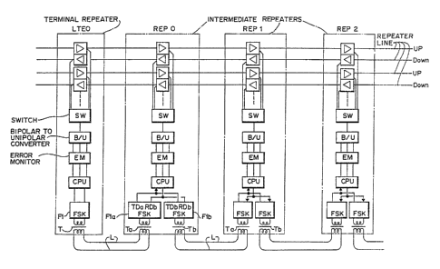
4 is a block diagram o~ a primary group
transmission line system according to the
present invention. In FIG. 4 LTE0 is a terminal
repeater operating as a supervisory terminal,
and REP0, REPl, REP2, ... are intermediate
repeaters in the transmission line (inter office
l; junction line). Each repeater (terminal and
intermediate) comprises an amplifier, and the
-transmission line is a bi-directional 2-wire
transmission line. Therefore, the amplifier
comprises a pair or amplifiers such as
-amplifiers-Tl for an up-line of the 2-wire line,
and amplifier Rl for a down-line of the 2-wire
line. Because the transmission lines include
several lines a plurality of amplifiers T2, R2,
T3, R3, etc. are required.
As shown in FIG. 5, each ampli~ier
includes a three coil transformer such as
transformer T12. Each transformer provides a
monitor output signal such as Ml. A swi~ch SW
selects a monitor output signal from among those
output by the amplifiers Tl, Rl, T2, etc. A
converter B/U converts a bipolar output of the
switch SW (the transmission line transmits
bipolar signals, i.e., an AMI signal) into a
unipolar signal. An error monitor EM obtains an
'
~7~
- 9 - 21.1~60
error rate based on the received output of the
c~nverter B/U.
In FIG. 4, reference letters CPU
designate a central processor unit; reference
letters FIa, FIb identify FSA interface
modulator/demodulators for frequency shift
keying; and reference letters Ta and Tb denote
transformers. These elements form a FSK modem
monitoring unit.
Each of the intermediate repeaters
REP0, REPl, REP2, etc. has the same structure.
The terminal unit LTE0 is slightly different but
also includes a central processor unit CPU, a
FSK interface FI and a transformer T. These
elements, however, operate as a supervisory
terminal unit. As shown in FIG. 4, each
transformer is cascade-connected in the
sequence: transformer T of supervisory terminal
unit LTE0 and transformer Ta of intermediate
repeater REP0-; transformer Tb of intermediate
repeater REP0 and transformer Ta of intermediate
repeater REPl, etc. In this case, the
supervisory line L is a 2~wire bi-directional
transmission line.
Referring to FIG. 5, the amplifiers T
and Rl of each repeater include input
transformers Tll and T21, and output
transformers T12 and T22. As noted above, the
output transformers T12 and T22 are three-coil
type transformers. In transformer T12, one coil
provides the monitor output signal Ml, and in
transformer T22 one coil provides the monitor
output signal M2. The switch SW (FIG. 4)
selects one of these monitor output signals.
~27~
- 10 - 21.1460
As shown in FIG. 4, error rate
information can be provided by each repeater
(terminal and intermediate). This information
can be accessed by the CPU of a terminal unit,
for example, the unit LTE0. This is
accomplished by a pair of FSK modems in each
intermediate repeater and cascade connecting
these modems. Since the information on the
supervisory line is FSK-modulated at each
repeater, the distance between repeaters can be
extended. Also, data on each transmission line
can be directly monitored by an error monitoring
circuit EM which monitors outputs Ml and M2 from
transformers T12 and T22 ~or the existence of
data errors. Such supervision/monitoring takes
place while the transmission line is in a
normal, in-service condition.
The structure and operation of the
supervisory system according tG the present
invention will be explained with reference to
FIGS. 4-8. The system extrac~s only one monitor
output signal while the transmission line is in
a normal, in-service condition. Specifically,
the analog switch SW can selectively provide any
one of the monitor output signals (Ml, M2) to
the converter B/U. The converter B/U applies
the converted unipolar signal to the error
monitor EM as shown in FIG. 7. FIG. 6(a)
illustrates a monitor output signal M and FIG.
6(b) illustrates an output o~ the converter B/U.
The error monitor EM detects H (high) and L
(low) levels output by the B/U converter, using
a clock signal CLK recovered by the converter
B/U (FIG. 6(c)). The error monitor EM detects
~2~
~ 21.1460
error rates such as input OFF, 10-3 error 10-4
error and 10-5 error (see, e.g., FIG. 12).
The error monitor EM provides signals
that are alternatively positive and negative
pulses in the form of an AMI signal. If two
positive pulses or two negative pulses appear in
succession, this is detected as an error. The
designation 10-3 means that an error is
generated once in 103 pulses. The error monitor
EM generates an output L (low) level under a
normal (no error) condition, and generates an
output H (high) level under an alarm (error)
condition. The processor ~PU detects the
outputs of the error monitor EM and provides
conditional information in a format such as
shown in FIG. 6(d). FIG. 6(e) illustrates an
output of the FSK interface FI. FSK-modulation
of a data "1" is represented by a sine wave of
1.3 kHz and FSK-modulation of a data "0" is
represented by a sine wave of 2.1 kHz.
The error monitor provides a coded
output comprising six bits of data as indicated
in FIG. 12. As shown, the six bit output
indicate: input OFF (no signal), 10-3, 10~4,
10-5, 10-6 and 10-7. The CPU encodes each six
bit output pattern received from the error
monitor EM into a three bit code as indicated in
FIG. 12. This three bit code is provided by the
CPU as shown in FIG. 6(d), together with a
destination (send) address, a repeater number
(REP0, 1, 2, etc.) a line number to be monitored
(Tl, Rl, T2, R2, etc.). This data is
transmitted by the CPU as conditional data.
~7~
- 12 - 21.1460
The processor CPU of the LTF0
supervisory terminal provides, over the
supervisory line L (FIG. 4), information such as
the repeater number and the line number to be
monitored in order ts monitor a desiynated line
(amplifier) ln a designated repeater (terminal
or intermediate). The processor of the
supervisory terminal repeater collects the
conditional information in the sequence of, for
example, line number Tl of LTE0, line number Tl
of REP0, line number Tl of REPl ... line number
Tl of REPn, line number Rl, of LTE0, line number
Rl of REP0 ... line number Rl of REPn. With
this sequence, the conditional data format is
essentially the same as that obtained by
eliminating the SEND ADDRESS shown in FIG. 6(d),
because the repeater number has the same value
as the SEND ADDRESS.
Each repeater detects and receives the
information transmitted, via the supervisQry
line L, by the CPU in LTE0. If a repeater
detects its repeater number in the in~ormation,
it transmits, to the supervisory terminal (e.g.,
LTE0), the conditional information of the
designated line together with a destination
(send) address which is that of the supervisory
terminal. If a repeater detects a repeater
number other than its own in the information, it
sends (repeats) the information to the next
repeater. Since the level of the signal
provided by each FSK modem (e.g., FIa, FIb) is
0 dB, the result is that the signal is
substantially amplified. The problem of
attenuation of the supervisory signal is thus
.
- 13 - 21.1~60
eliminated. As a result, the supervisory line
can be extended indefinitely.
Moreover, monitoring of any amplifier
and the transmission line can be performed while
the line is in a normal, in-service condition,
because a particular test signal is not used on
the transmission line. In addition, a line in
the non-busy condition can also be monitored
since an idle signal is usually transmitted
while a line is in such a condition.
When error rates as small as 10-3,
10-4, ... 10-7, are detected, the process of a
line deteriorating can be monitored. Effective
and timely maintenance can therefore be
performed.
In a system of the present invention,
a monitor output signal is provided by an output
transrormer as indicated in FIG. 5 or the
monitored signal can be provided by a pulse trio
signal generator. Therefore, the present
invention is compatible with existing systems
using pulse trio signals, thus minimizing the
cost of providing the present invention to
existing systems.
FIG. 7 is a block diagram of a
repeater according to the present invention,
such as the terminal repeater LTE0. FIG. 7
illustrates 36 2-wire lines, 36 pairs of
amplifiers Tl, Rl, .~. T36 and R36 are needed
for these lines. These amplifiers provide 72
monitor output signals. The analog switch SW
selectively provides a designated one of the 72
monitor output signals.
- 14 - 21.1460
In FIG. 7 the reference letter Q
designates a switch comprising an n-channel FET
and a p-channel FET connected in parallel; and
reference letter I designates an inverter for
generating an inverted signal. As shown in FIG.
7, a switch Q and an inverter I can be provided
for each monitor output signal. Each switch Q
is controlled by a corresponding one of the
selected outputs ~ 2~ --, Y72 generated by
an address decoder AD which designates the
monitor output siynal to be applied to the
transformer TT. The designated, i.e., selected,
monitor output signal is applied to tho
bipolar/unipolar converter B/U through a
transformer TT. A buffer 1 (e.g., FI~. 8)
provides address information to the address
decoder AD. The buffer 1 receives the address
information rrom the CPU, which in turn receives
the address information from the FSK interface
which includes, for example, an FSK modem, a
band-pass-fil~er and a transformer. A
supervisory terminal (e.g., LTE0), supplies
address si~nals via its CPU to the address
decoder AD of the supervisory terminal through a
buffer similar to buffer 1.
FIG. 8 is a block diagram of a
transmitter/receiver of a supervisory terminal
according to the present invention. In FIG. 8,
Ta and Tb correspond to the transformers
explained with reference to FIG. 4 and CPU
corresponds to the processor shown in FIG. 4.
Duplexers DUP 103a and 103b function as
branching circuits to separate the receive
signals and the send signals on the supervisory
- 15 - 21.14~0
line L. This c~rcuit comprises, for example, a
2-wire/4-wire convertin~ circuit. Filters lOla,
102a, lOlb and 102b filter different frequencies
of FSK modulated signals, which are sent from
and received by the duplexers DUP 103a and 103b.
Limiters LMT 104a and LMT 104b shape sine waves
respectively output from the filters 102a and
102b, into rectangular waves in accordance with
an input mode re~uirement of FSK modems lOOa and
lOOb. Carriers detectors CD lO5a and CD 105b
detect carrier frequencies in the FSK signal
applied on the supervisory line L. These
carrier detectors generat~ a L level output
indicating detection of a carrier and a H level
output to indicate non-detection of a carrier.
The FSK modems lOOa and lOOb convert an analog
FSK signal into a digital signal. In FIG. 8,
reference letters CG represent a clock generator
which generates a clock signal having a
frequency of 3.68 MHz and provides this signal
as a clock that drives the FSK modems lOOa and
lOOb and the processor CPU.
Next, operations are explained with
reference to FIGS. 8-11. While the CPU (FIG. 8)
is in a waiting condition, the CPU sets both
SETa and SETb to a H level. This places the FSK
modems lOOa and lOOb in a receiving condition.
When an FS~ signal is received by the
transformer Ta (which in turn receives them
Erom, for example, LTE0), this signal is
provided by the duplexer DUP 103a to filter
102a. FIG. 9(a) illustrates a signal provided
by DUP 103a or 103b. After filtering by, for
example, filter 102a, noise is eliminated from
: , . : .
., ' .
- 16 - 21.1460
the FSK signal and the filtered signal
corresponds to, for example, the 1.3 kHz or the
2.1 kHz sine waves shown in FIG. 9(b). That is,
it represents a data "1" or a data "0". The
filtered sine wave is applied to the limiter LMT
104a, which shapes the input waveform into a
rectangular wave (shown in detail as a
trapezoidal wave in FIG. 9(c)). This
rectangular waveform conforms to an interface
requirement of the input terminal RCa of the E'SK
modem lOOa (FIG. 8).
The shaped (rectangular) signal shown
in FIG. 10 (and FIG. 9(c)) is applied to the
carrier detector CD 105a (FIG. 8) which provides
an output CDa. When CDa is a L level, CPU sets
the output SETa to a $ level in order to set
ACTa of FSK modem lOOa to the H level and to
place the FSK modem lOOa in the receiving mode.
The CPU also sets the output SETb to the L level
in order to place the FSK modem lOOb in a non-
receiving mode (send mode). Therefore, an
output of NAND gate 107 becomes a H level and
the input ENb of FSK modem lOOb becomes a H
level, stopping operation of the FSK modem lOOb.
Simultaneously, the output of RDb is set to a H
level, enabling the AND gate 106 to provide the
output RDa of FSK modem lOOa to the RD terminal
of the CPU. An output of NAND gate 108 becomes
a L level, setting ENa to a L level, placing FSK
modem lOOa in the operating condition.
Accordingly, the FSK modem lOOa converts the
analog FSK signal applied to terminal RCa into
digital signals (e.g., 1 and 0) and then outputs
these digital signals to the CPU through the
~L2~
- 17 - 21.1460
terminal RDa. After receiving the converted FSK
signal, the processor CPV places the FSK modems
lOOa, lOOb into a waiting condition.
The processor CPU receives a command
via a RD input to provide a designated monitor
output to a supervisory terminal. In response,
the CPU sends an address signal (information) of
the designated line (amplifier) to the address
decoder AD to select the error monitor output
signal of the designated line (amplifier). The
selected error monitor output signal then passes
through the switch SW and transformer TT to the
error monitor EM through the converter B/U (FIG.
7).
Referring to FIG. 11, the error
monitor EM outputs a coded error signal ~FIG.
12) to the processor. As discussed above, the
CPU provides a three bit representation af this
coded error signal together with other
information in a format as shown in FIG. 6(d3.
The CPU then sets output SETa to a L level in
order to set the FSK modem lOOa to the sending
condition. The FSK modem lOOa can therefore FSK
modulate the conditional information ~FIG. 6(d))
from the CPU and output the conditional
information to the transformer Ta. The
conditional information therefore is transmitted
from the CPU output terminal TD through the FSK
modem lOOa, filter lOla, DUP 103a and the
transformer Ta. In this case, SETb is set to a
L level to prevent receiving FSK signals ~rom
the transformer Tb.
~ 2~
- 18 - 21.1460
If the FSK signal present at the
transformer Ta is not a command for the
repeater, the CPU sets SETa to a H level and
SETb to a L level. The FSK modem lOOb is
thereby set to a sending condition. The CPU
then sends (repeats) the information received
via transformer Ta to Transformer Tb and thus to
the next repeater.
FIG. 13 is a circuit diagram o~ the
FIG. 8 system. In FIG. 13, the duplexers 103a
and 103b respectively comprise 2-wire/4-wire
converters. These converters comprise a pair of
operational amplifiers. The filters lOla, 102a
and lOlb, 102b are switched capacitor filters
that are switched by clock signal CLK. The
clock signal CLK can have a frequency of, for
example, 153.5 kHz. This frequency can be used
to detect signals having frequencies of Z.2 kHz
or less and it can be obtained by, for example,
dividing an output of the oscillator CG.
The limiters 104a and 104b function as
sine wave/rectangular wave converters which
convert the output of filters 102a and 102b into
rectangular waves having a duty cycle of
approximately 50%. Each limiter comprises one
comparator.
The carrier detectors CD 105a and 105b
respectively convert the outputs of filters 102a
and 102b into rectangular waves and also add a
bias level to these signals. The carrier
detectors integrate the converted signals using,
for example, a RC network, and detect a DC level
dif~erence between a reEerence signal and the
integrated signal. The DC level difference
~Z~78~
- 19 - 21.1460
represents the presence or absence of a carrier.
The time required to detect a carrier signal is
therefore determined by the time constant of the
integration RC network.
The FSK modems lOOa and lOOb can
comprise any commercially available LSI modems.
Generally, when demodulating a signal, the
conversion is performed on an input signal
having approximately a 50% duty cycle.
FIG. 14 is a block diagram of a
supervisory terminal repeater of the present
invention; and particularly of a
transmitter/receiver of the terminal repeater
LTE0 of FIG. 8. As shown in FIG. 4, the LTE0
includes an FSK modem FI. As noted above, the
LTE0 ~unctions as a supervisory terminal and
collects conditional information from each
repeater. The construction of the LTE0
transmitter/receiver is difierent from that of
the intermediate repeaters.
When the CPU transmits a polling
signal ~e.g., the address of a repeater) to one
of the intermediate repeaters, the CPU f~rst
checks if a signal CDa is a H level. If it is,
the CPU sets an output SETa to a L level. This
places the FSK modem lOOa in a sending
condition. When the CPU is not polling, it sets
the FSK modem lOOa to a received condition by
setting the output SETa to a H level.
If the signal CDa changes from a H
level to a L level, the CPU receives conditional
information from FSK modem lOOa via RD, and
checks the repeater number and line number
included in the information (e.g., FIG. 6(d)).
~78~
- 20 - 21.1460
A main memory MM, stores conditional
information for each repeater and line (i.e.,
each amplifier) that has been collected by the
CPU over a series of polling operations for each
repeater and line (i.e., each amplifier). This
conditional information is stored at memory
locations set aside for each repeater and line.
The CPU also collects error monitor information
from its own amplifying circuits by operating
the switch SW (FIG. '7). The collected
conditional information is stored in the main
memory MM via a common bus.
Terminal repeater LTE0 (FIG. 14)
functions, as noted above, as a supervisory
lS terminal repeater. The repeater LTE0 includes a
keyboard KB and a display unit (CRT controller,
and CRT display). An operator uses the keyboard
to send commands to the CPU of the LTE0 via I/O
interface 1 and the common bus. Any conditional
information for an amplifier within a particular
repeater of the system can be accessed.
Conditional information relating to the status
o~ each amplifier or part of the system is
collected and stored in the main memory MM. The
collected conditional information can be
displayed on the CRT via the common bus and I/O
interface 2.
As explained above, the present
invention provides the advantages that (1) an
error monitor can be utilized for repeaters
while they are in a normal, in-service
condition, (2) the supervisory line length can
be extended since each repeater transmits a
received signal to the next repeater, (3) there
~Z7~
- 21 - 21.1460
is no restriction on the number of frequencies
as in the existing system, since a particular
repeater and line (i.e., an amplifier) within
the repeater are desiynated b~ an address
instead of a frequency, and (4) the present
invention is compatible with the pulse trio
system used in existing systems.