Note: Descriptions are shown in the official language in which they were submitted.
7~37~
-1- RCA 80,698
AUTOMATIC GAIN CONTROL OF A SCRAMBLED VIDEO SIGNAL
This invention concerns apparatus in a
subscription television system for processing a scrambled
broadcast type television signal such as a television
signal having a suppressed synchronizing component. In
particular, this invention concerns such apparatus
operatively associated with automatic gain control (AGC)
circ~its of a television receiver to reduce the cost and
complexity of a video signal decoder which provides a
descrambled television signal to signal processing circuits
of the receiver.
In subscription television systems television
programming signals are transmitted either "over the air"
or through a suitable cable network, in scrambled form.
Such signals may be descrambled for viewing by means of a
suitable decoder associated with the television receiver of
an authorized system subscriber. The decoder is usually
situated in a converter unit located external to the
television receiver. The programming signals may be
grouped into several levels, or tiers, each representing a
different programming category such as sporting events,
movies, etc. The decoder of a particular subscriber is
authorized to descramble the televised programming signals
in selected categories, with the televised programming
signals in remaining unauthorized categories being coupled
to the television receiver in an unviewable scrambled form.
A horizontal synchronization suppression
technique is commonly used to scramble a broadcast
television signal. In such a "suppressed sync" techni~ue,
scrambling is accomplished by suppressing the horizontal
image synchronizing (sync) pulse component of the
television signal. This causes the horizontal deflection
system of the receiver to lock onto random video signal
peaks during the active video line trace interval, rather
than locking onto the actual horizontal sync pulses,
thereby producing an unstable, unviewable displayed image.
Each system subscriber is provided with a decoder
unit whose "front end" circuit includes conventional
~%7~
-2- RCA 80,698
tuning, interm~diate frequency (IF) and video detection
stages. Also, a gated automatic gain control circuit,
adapted for responding to the tips of horizontal sync
pulses, is provided within the decoder for controlling the
gain of the ~uning and IF stages in accordance with the
output of the video detection stage.
A sync restoration circuit operates during the
suppressed sync pulse interval of the video signal
developed at the output of the video detector stage for
1~ producing standard horizontal sync pulses. These sync
pulses are continuously inserted in the video signal
developed at the output of the video detector stage for
producing a descrambled video signal suitable for viewing.
An AGC voltage derived from some recurrent parameter in the
scrambled signal is applied to AGC circuits in the decoder.
The descrambled video signal with restored sync
pulses is afterwards impressed on a standard television
channel RF carrier signal by means of an RF modulator. It
is then coupled as a descrambled RF television signal to an
antenna input of the television receiver. Each decoder may
additionally include a decode au-thorization circuit storing
a unique subscriber code. This unique code is compared to
a subscriber authorization code transmitted during a
horizontal line of the vertical interval of the broadcast
television signal~ I~ the s-tored subscriber code and the
transmitted subscriber authorization code compare
favorably, a decode authorization si~nal is developed for
enabling the decoder, the decoder otherwise being disabled.
Decoder systems for descrambling a suppressed sync video
signal are discussed in US patent 4,408,225 - Ensinger, et
al., ~or example.
The size, cost and complexity of a suppressed
sync video signal decoder are increased by the need for the
decoder to include a tuning stage, IF stage, video detector
stage, AGC stage and RF modulator, which stages (~xcept for
the modulator) duplicate stages already found in the "front
end" of a television receiver. Thus it is desirable to
provide a decoder which does not re~uire such stages.
337~
-3- RCA 80,69~
Accordingly, the Electronic Industry Association (EIA) of
the United States has proposed a decoder-receiver interface
standard which simplifies the design of decoders for use in
suppressed sync television signal systems by eliminating
the need for the aforementioned tuning, IF, detector, AGC
and modulator stages in a suppressed sync decoder unit. As
outlined in EIA Consumer Products S-tandard IS-15 "NTSC
Television Receiver Audio/Video Baseband Interface
Specification," the EIA decoder standard provides a
mutually agreeable convention, to both television receiver
manufacturers and the subscription TV industry, for the
implementation of a standarized sync suppressed video
decoder system.
In the case of a suppressed sync signal, a
receiver having AGC circuits which respond to the sync tip
level is unable to properly provide automatic gain control.
Thus it is desirable for a suppressed sync signal decoder
to be able to provide information to the receiver
concerning the amount of automatic gain control re~uired
~0 for proper gain control under suppressed sync conditions.
To this end the EIA standard sets uniform specifications
for the decoder, particularly with regard to decoder output
specifications.
The EIA standard provides decoder voltage and
~5 impedance conventions with respect -to video input, video
output, and AGC requirements to assure compatibility with
various receiver operating requirements. The EI~ s-tandard
is intended to permit control of a television receiver's
AGC circuits in a manner which eliminates the need for
tuner, IF, detector, AGC and modulator stages in the
suppressed sync decoder unit. An additional benefit of a
decoder developed in accordance with the EIA standard is
that a viewer can retain full use of a television receiver
remote control unit, which is not the case with systems
using decoders of conventional design.
In accordance with the present invention, there
is disclosed herein a video signal descram~ling system,
illustratively including a sync restoration network,
~7i~
-4- RCA 80,698
comprising an interface circuit for coupling a video siynal
output of a suppressed sync type decoder to existing AGC
circuits of the receiver for controlling the gain of the
video signal, without needing tuning, IF, detector, AGC and
modulator stages in the decoder. The interface circuit
monitors the level of a restored sync pulse from the
decoder and genera-tes a control signal indicative of
whether or not the video signal gain (i.e., peak-to-peak
amplitude~ is correct. The control signal is applied to
e~istin~, conventional AGC ci.rcuits of the receiver for
controlling the video signal gain. The receiver AGC
circuits, decoder and interface circuit interact such that
the control signal from the interface circuit continuously
au~nents the normal gain control action of the AGC circuits
in the receiver for esta~lishing a correct video signal
gain in the presence of a received suppressed sync video
signal.
In the Drawing:
FIGURE 1 shows a portion of a television receiver
~0 and video signal gain control apparatus according to the
present invention, as well as suppressed sync restoration
apparatus;
FIGURE 2 illustrates signal waveforms helpful in
understanding the operation of the sync restoration
apparatus of FIGURE 1;
FIGURE 3 shows a network, in block diagram form,
suitable for use in a suppressed sync decoder included in
the system of FIGURE l;
FIGURE 4 depicts a simplified version of a
3~ poxtion of AGC circuits of the receiver;
FIGURE 5 illustrates a transfer charac-teristic of
an AGC detector associated ~7ith the receiver AGC circuits;
FIGURE 6 is a table summarizing operatin~
characteristics of the disclosed sync restoration and gain
control apparatus; and
FIGURE 7 illustrates the transfer characteristic
of a decoder interface network included in the system of
FIGURE 1.
~27~33~
-5- RCA 80,698
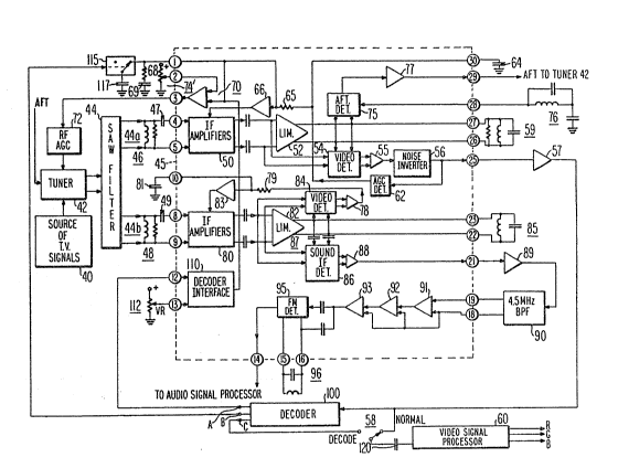
In FIGURE 1, a source 40 is a source of RF
television (TV) signals which include suppressed sync
scrambled RF TV signals such as may be provided by a cable
TV subscription service. The RF signals from source 40 are
coupled to a television receiver, e.g., including a tuner
42, filter 44 and other units as will be discussed, where
it is demodulated to produce scrambled video and sound
representative signals. A decoder unit 100, external to
the receiver, restores the sync component of the scrambled
1~ video signal. The restored sync (unscrambled) video signal
is processed by the receiver in a conventional fashion to
produce an image. As will be explained in detail later,
the receiver includes provision for controlling the signal
gain o~ the tuner RF stage and the IF stage in t~e presence
of scrambled, suppressed sync signals. In this manner
separate tuner, IF and AGC stages need not be provided in
decoder 100.
More specifically, in FIGURE 1 tuner 42 receives
the RF signals from source 40 and selectively translates
the RF signal of a selected TV channel to an intermediate
freguency ( IF) signal including video and sound carriers
at, e.g., 45.75 MH7 and 41.25 MHz, respectively. The IF
signal includes an amplitude modulated (AM) video carrier
of the vestigial side~and type representing the composite
video information, and a frequency modulated (FM) sound
carrier containing the sound information.
The IF output signal from tuner 42 is coupled via
a preamplifier and an adjacent channel sound trap (not
shown) to inputs of a dual channel IF surface acoustic wave
(SAW) filter 44 such as the T1802 SAW filter available from
Toshiba Corporation. The IF signal from tuner 42 is split
into two separate channels for sound and video information
demodulation in accordance with the quasi-parallel
principle via the dual channels of SAW filter 44, each
channel exhibiting a bandpass response around the
respective carriers. A first differential output 44a of
SAW filter 44 associated with the video channel is coupled
to signal input terminals 4 and 5 of a network 45 included
~27~37~
-6- RCA 80,698
e.g., in an integrated circuit, via an
inductance-resistance circuit ~6 which tunes out the
capacitance normally associated with the SAW filter
output, and via an AC coupling capacitor 47. The video
channel portion of SAW filter 44 associated with outpu-t
44a exhibits a response which matches the vestigial
sideband video component of the IF signal and which
attenuates the 41.25 MHz sound carrier signal.
The quasi-parallel sound channel portion of SAW
1~ filter 44 associated with a differen-tial output 44b is
coupled to signal input terminals 8 and 9 of network 45 in
the same manner as the video component via an
inductance-resistance circuit 48 and an AC coupling
capacitor 49. The sound channel portion of SAW filter 44
exhibits a double tuned response with a first peak
amplitude response at the sound carrier frequency and a
second peak amplitude response at the video carrier
frequency.
In the video IF channel, the video component of
the IF si~nal at input terminals 4 and 5 of network 45 is
coupled to an IF amplifier stage 50 which includes plural
gain controllable IF amplifiers. The amplified video
component from stage 50 is AC coupled to a limiter 52 and
to a video detector 54 (e.g., a four quadrant
~5 multiplier). A bandpass filter tank circuit 59 coupled
via terminals 26 and 27 to the output of limiter 52 is
tuned to the video carrier frequency of 45.75 MHz.
Limiter 52, filter 59 and video detector 54 form a
synchronous detector for producing a baseband composite
video signal at the output of detector 54. The composite
detected video signal is coupled via an amplifier 55 to a
noise inverter 56 which in this case inverts black-going
blanking interval noise pulses below a given threshold
level to prevent the noise pulses from disrupting the
operation of subsequent sync separator circuits, and to
prevent the noise pulses from interfering with automatic
gain control (AGC) action.
The baseband video signal output of noise
inverter 56 is coupled via a terminal 25, a buffer
. .
~7~37~
-7- RCA 80,698
amplifier 57 and a switch 58 to a video signal processor 60
including, e.g., sync separator, luminance and chrominance
fre~uency selection, and luminance and chrominance
processing circuits for developing R, G, B color image
representative signals as known.
The baseband video output signal from noise
inverter 56 is also coupled to an AGC peak detector 62
which peak detects the horizontal sync componen-t of the
baseband video signal to develop an AGC control voltage
related to the magnitude of the sync component. This AGC
control voltage is developed across a filter capacitor 64
coupled to a terminal 30 of circuit 45.
The AGC voltage is also coupled via a current
determining resistor 65 to an AGC filter network including
a resistor 68 and a storage capacitor 69 connected to
terminal 1 of circuit 45. An AGC control voltage appearing
at terminal 1 is coupled via an AGC amplifier 66 to a gain
control input of IF amplifier stage 50 for controlling the
gain of the amplifiers within stage 50 in accordance with
~0 the level of the detected sync pulse to maintain a desired
si~nal gain for the video IF channel.
The AGC voltage at terminal 1 is also applied -to
an RF AGC comparator amplifier 70, which provides an
amplified AGC voltage to a gain control input of tuner 42
~5 vià an RF AGC circuit 72. RF AGC circuit 72 is of
conventional design and includes a comparator responsive to
a reference voltage and to the AGC voltage derived from
terminal 1 for providing an ou-tput gain control signal
which determines the gain status (e.g., minimum or maximum
gain) of tuner 42. A potentiometer 74 coupl~d via a
terminal 2 to a reference input of comparator 70
establishes the operating threshold of RF AGC comparator 70
to determine the point at which comparator 70 conveys the
AGC control voltage to circuit 72.
An automatic fine tuning (AFT) peak detector 75
is operatively associated with a bandpass filter tank 76
tuned to the 45.75 MHz video carrier. Detector 75 responds
to the amplitude limited video IF carrier signal from
3~7~
- 8 - RCA 80,698
limiter 52 for developing an AFT voltage which is coupled via
a buffer amplifier 77 and a terminal 29 to an AFT control
input of tuner 42 to maintain proper tuning of tuner 42.
In the sound IF channel, the IF signals at
terminals 8 and 9 including sound and video components is
coupled to an IF amplifier stage 80 which includes plural
gain controllable amplifiers. An amplified IF signal from
stage 80 is AC coupled to a limiter 82, to a video IF
detector 84, and to a sound IF detector 86 via a capacitive
phase shifting network 87. Detectors 84 and 86
illustratively comprise four ~uadrant multipliers. A
bandpass filter tank 85 coupled via terminals 22 and 23 to
the output of limiter 82 is tuned to the video IF carrier.
Limiter 82, detector 86 and tank 85 form a mixer for
providing a 4.5 MHz FM intercarrier sound signal from the
sound and video components of the IF signal. The
intercarrier sound signal from detector 86 is coupled via an
amplifier 88, a terminal 21, a buffer 89, a 4.5 MHz bandpass
filter 90 and terminals 18 and 19 to a limiter network
comprising cascadad progressive limi~ing stages 91, 92 and 93
which provide an amplitude limited FM intercarrier sound
signal to an FM detector 95. Detector 95 operates together
with a discriminator tank circuit 96 coupled to terminals 15
and 16 for generating a demodulated baseband audio signal.
The audio signal is applied to an audio signal processor
stage (not shown) including audio amplifiers.
Automatic gain control of the sound IF channel is
achieved in response to a control voltage derived from the
output of video IF detector 84. The detected output signal
o~ detector 84 îs coupled via an amplifier 78, a low pass AGC
filter including a resistor 79 and a capacitor 81 coupled to
a terminal 10, an AGC amplifier 83 to a yain control input
of sound IF amplifier stage 80.
The system of FIGURE 1 also includes a suppressed
sync decoder 100 designed in accordance with the proposed
EIA standard. The baseband composite video signal from
~ 3~
- RCA 80,698
terminal 25 of circuit ~5 is applied to a signal input of
decoder 100 via buffer 57 which exhibits a suitable output
driving impedance, e.g., 75 ohms. A baseband video signal
"A" with a restored horizontal sync component is provided
from one output of decoder 100 to a decoder interface
network 110 in circuit 45 via an input terminal 12.
Interface 110 includes a comparator circuit for developing
an output control signal which modifies the charge on AGC
filter capacitor 69 and augments the action of the video
AGC circuits particularly in the presence of received
suppressed sync signals. A potentiometer 112 coupled to
terminal 13 provides a reference voltage VR to a reference
input of the comparator in interface 110.
A DC voltage "B" provided from another output of
decoder 100 controls the operation of an electronic switch
115 to which a filter capacitor 117 is coupled. In the
absence of decoder 100, no DC voltage is applied to switch
115 and capacitor 117 is decoupled from the AGC fil-ter
network including resistor 68 and capacitor 69. When
decoder 100 is connected to the system, control voltage "B"
causes switch 115 to be placed in the position shown
whereby filter capacitor 117 is connected across AGC filter
capacitor 69, thereby increasing the AGC time constant
associated with video signal AGC action. The longer AGC
time constant is necessary for stability when the decoder
is active to compensate for normally expected signal
processing delays (as large as 1 millisecond, or five
horizontal lines) inherent in the operation of the decoder
and recognized by the EIA standard. The normal, faster AGC
time constant using filter capacitor 69 alone represents a
compromise between a need for a time constant fast enough
to accommodate a channel change condition, and a time
constant slow enough to be immune to -the effects of
aircraft induced "flutter".
An output signal "C" from decoder 100 is a
restored sync video signal developed as will be described
below. The decoder output lines on which restored s~nc
video signals "A" and "C" appear could be connected
~7~3~
-10- RCA 80,698
together internal to decoder 100 so that a single decoder
output line results. However, some systems may require two
separate decoder output lines, e.g., with one output line
(C) conveying a signal with both restored sync and video
information to be displayed, and another output signal line
(A) conveying a composite synchronizing signal with
restored sync but without video information, for a
speciali~ed use. In this example decoder output signals A
and C are similar restored sync video signals containing
in~ormation to be display~d.
Restored sync decoder output signal C is
selectively coupled to video signal processor 60 via switch
58 and an AC coupling capacitor 120. Switch 58 can be a
manual viewer controlled switch, or a microprocessor
controlled electronic switch responsive to both user
selection signals and automatic control signals received
from the decoder, depending on the characteristics of a
particular decoder system. Switch 58 is placed in a DECODE
position when decoder 100 is present and operative to
~0 decode a received suppressed sync television signal.
Switch 58 is placed in a NORMAL position when deGoder 100
is absent or inoperative in the presence of a received
television signal with proper (non-suppressed) sync.
In the presence of a suppressed sync television
~5 signal, the input signal to decoder 100 always exhibits
suppressed sync because the decoder input signal line is
not included in the sync restoration control loop.
Briefly, the decoder input line receives only a suppressed
sync signal via output 4~a of SAW filter 44, IF amplifiers
50, video detector 54 and buffer 57. One decoder output
line provides a restored sync video signal C to video
processor 60, and another decoder output line provides a
restored sync video signal A to AGC circuits of the
receiver via interface network 110 for maintaining correct
receiver signal gain.
The operation of decoder 100 in conjunction with
interface 110 and the AGC circuits of the receiver will now
be described in detail.
~27~3'7~
~ RCA 80,698
Decoder 100 and the video AGC circuits of the
receiver form an automatic gain control system for
suppxessed sync signal conditions. In accordance with the
EIA standards a video signal gain change is not re~uired
when the sync tip voltage is +1.0 volt. ~ gain change is
required, however, when the sync tip voltage is more or
less than +1.0 volt. More specifically, a gain change is
not required when "GM" as defined in expression (1) below
is substantially equal to unity, but a gain change is
l~ required when GM is other than unity:
GM = 2.143v. - l.Ov.
2.1~3v. - DRS (1)
where
GM is a gain multiplier factor;
2.143v. is the voltage associated with the 120
IRE video signal level (zero carrier voltage);
1.0 v. is the desired sync tip voltage level; and
DRS is the actual sync tip voltage of a decoder
restored sync component from the output of decoder 100.
~0 When expression (1) is solved for the term DRS,
expression (2) below results:
DRS = 2.143v. - 1.143v.
GM (2)
If the gain is ~rong, e.g., too high as is typical for a
~5 suppressed sync signal, the decoder will produce an output
DRS level (during the sync in-terval) of less than +l.0
volt, for example. This DRS level is sensed by interface
llO which then acts to modify the charge on AGC capacitor
69 as required to produce a desired correct video signal
gain and an attendant DRS sync tip voltage of approximately
~1.0 volt. This is accomplished by means of comparator and
current source circuits in interface network 110. The
decoder itself does not produce a "correct" DRS sync tip
level of +1.0 volts immediately upon receipt of a
suppressed sync video signal, because the receiver would
then have no means of knowing whether or not the video
signal gain should be changed.
~2~
-12- RCA 80, 698
Various techni~ues are known ~or developing a
suppressed sync signal. FIGURÉ 2 illustrates waveforms
representing both one type of a suppressed sy~c signal, and
a decoder res-tored sync (DRS ~ output signal from decoder
100. In the suppressed sync signal the normally nega-tive
going (below 0 IRE ) horizontal sync component has been
replaced with a 1 M~Iz burst marker of approximately 80 IRE
peak-to-peak amplitude centered between the 0 IRE and 100
IRE levels. If the amplitude of the received suppressed
sync signal is correct, the ao IRE burst marker will cause
a given voltage to be produced when peak detected, as will
be discussed subsequently. Otherwise, under incorrect gain
conditions, the amplitude detected burst marker will cause
another voltage, si~nifying that a ~ain change is required
to be produced. The decoder restored sync ~DRS) output
signal ~rom decoder 100 has a negative-going restored sync
component of a magnitude which signifies to the receiver,
via interface network 110, the amount of signal gain change
re~uired, if any.
FIGURE 3 illustrates a portion of a decoder
arrangement suitable for restoring the sync component of a
suppressed sync signal as shown in FIGURE 2.
In FIGURE 3, a suppressed sync video signal of
the burst marker type i5 filtered by a bandpass filter 130
which passes the burst marker signal frequency. The
~iltered burst marker component is amplitude detected by a
peak-to-peak envelope detector 132, which provides an
output signal representative of the magnitude of the sync
interval burst marker component. It is extremely unlikely
that a false peak detector output will be produced by 1 MHz
video signal image interval compon~nts, since 1 MHz video
signal components are unlikely to appear with sufficient
energy ta produce an output from peak detectar 132
corresponding to the detected output produced by the
relatively high energy 1 MHz burst marker.
The detected burst marker from detector 132 is
applied to one input of a comparator 134, another input of
which receives a reference voltage VREF. The magnitude of
~:7~3~
-13- RCA 80, 698
the detected burst marker signal exceeds VREF under
substantially all expected conditions, whereby comparator
134 produces an output GATE timing signal coincident with
the sync interval. The GATE signal signifies the presence
of the sync interval, and is employed as will be discussed
below.
Recall from expression (2) discussed previously
that the sync tip voltage of the decoder restored sync
(DRS) signal from decoder 100 is given by
10DRS - 2.143v. - 1.143v
GM (2)
Gain multiplier factor GM is the ratio of the constant
peak-to-peak detected sync interval burst marker voltage
~Vl) which is expected to appear at the output of detector
132 under correct signal gain conditions to-the variable
peak-to-peak detected burst marker voltage (V2) which is
actually developed at the output of detector 132. Thus
expression (2~ can be rewritten as expressions (3) or (3a)
below:
20DRS = 2.143v. - 1.143v.
(Vl/v2) (3
or
DRS = 2.143v. - [ 1.143v./Vl ] V2 t3a)
Under correct video signal gain conditions Vl = V2, i.e.,
the burst marker amplitude is correct, whereby the DRS sync
tip level is ~1.0 volt as desired for correct video signal
gain conditions.
The transfer function represented ~y expression
(3a) can be implemented by means of the portion of the
network in FIGURE 3 including an amplifier 140 and a
differential amplifier 142.
Amplifier 140 translates detected signal V2 with
a constant amplification factor K=1.143/Vl, where Vl is a
constant. Amplifier 140 may act as an amplifier, an
attenuator, or as a unity gain amplifier for values of X
greater than unity, less than unity or unity, respectively.
~ 7 ~ 3 7 ~ RCA 80,698
The output signal from amplifier 140 is applied to an
inverting input (-) of a differential amplifier 142. A
reference voltage of -~2.143 volts is applied to a
non-inverting input l+) of differential amplifier 142.
Amplifier 142 provides an output DRS voltage in accordance
with expression (3a).
The DRS output voltage from amplifier 142 is
applied to one input of an electronic switch 145, another
input of which receives the suppressed sync video signal,
e.g., as derived from input circuits of decoder 100. The
position of switch 145 is controlled by the GATE signal
from the output of comparator 134 such that during each
sync interval switch 145 is placed in the position shown
for conveying the DRS voltage to the decoder output. At
other timesl when the GATE signal is absent, switch 145 is
placed in its other position whereby the remaining portion
of the video signal is conveyed to the decoder output.
Thus during each sync interval switch 145 substitutes the
DRS voltage from amplifier 142 for the burst marker in the
~0 suppressed sync video signal to thereby produce a video
signal with a restored sync component at the output of the
decoder.
As mentioned previously, the sync tip voltage of
the restored sync video signal will be substantially equal
~5 to ~l.0 volt under correct signal gain conditions, or less
than ~1.0 volt if the gain is too high, for example. The
latter condition will be sensed by interface network 110,
which will act to adjust the AGC circuits of the receiver
to produce a correct video signal gain. Under incorrect
video signal gain conditions, the AGC circuits of the
receiver will respond to a control current output of
interface network 110 related to the DRS output level of
decoder 100 for incrementally changing the video signal
gain toward the desired correct gain.
The AGC circuit action causes the amplitude of
the suppressed sync video signal applied to the input of
decoder 100 to incrementally approach the correct
peak-to-peak video signal amplitude, and the restored sync
~L2~3~
15 -- RCA 80, 698
component of video signals A and c from the output of
decoder 100 will incrementally approach the desired correct
value of +1.0 volt.
The operation of the receiver AGC system for both
normal and suppressed sync conditions is described in detail
below with regard to FIGURES 4-7.
FIGURE 4 depicts a simplified version of the
receiver video AGC system of FIGURE 1, wherein corresponding
elements are identified by the same reference number. AGC
detector 62, a negative peak detector, charges capacitor 64
with a voltage related to the magnitude of the
negative-going peaks o~ the detected baseband video signal,
i.e., thè sync tips in the case of a conventional television
signal. Resistor 65 converts the voltage on capacitor 64 to
a current I which represents a charging component of AGC
capacitor 69. A current I' conducted by a current source
associated with interface network 110 represents a
discharging component of capacitor 69. The magnitude of
current I' varieæ in accordance with the nature of a given
suppressed sync condition. A total AGC current IT equal to
the di~erence between currents I and I' represents the net
charging current of capaci~or 69 and serves to develop a
voltage across capacitor 69 which is conveyed to AGC
circuits of the receiver via amplifiers 60 and 70. Current
IT equals zero for correct gain steady state conditions.
AGC detector 62 exhibits a gain change vs.
current condition characteristic as shown in FIGURE 5. The
detector exhibits a linear gain change up to a gain
increase of +0.5 db and up to a gain decrease of -0.5 db,
and a nonlinear response for gain changes above and below
+0.5 db and -0.5 db. Detector 62 operates in a saturated
region in the nonlinear case, exhibiting either a positive
saturation current output Is(+) or a negative saturation
current output Is~-). In the saturated region the rate at
which the voltage on capacitor 69 is permitted to change is
restricted to help maintain the stability of the AGC
control loop. An AGC detector characteristic with linear
-16- ~27~37~ RCA 80,698
and nonlinear (saturated) regions such as that illustrated
is well known and widely used in television receiver AGC
systems.
With the decoder connected to the receiver under
suppressed sync condi-tions, correct video signal gain will
be established for steady state conditions. The internal
AGC system of the receiver alone would be unable to achieve
correct gain under suppressed sync signal conditions, and
would produce a video signa~ with too much gain. The
overall AGC system including the combination of decoder
100, interface 110 and the existing internal AGC system of
the receiver operates in a similar way to the way the
internal AGC system of the receiver operates alone under
normal, non-suppressed sync conditions to establish correct
gain. Under steady state conditions when correct gain is
achieved and the DRS sync tip voltage substantially equals
+l.O volt, current I conducted to terminal 1 from the
output of peak detector 62 substantially equals current I'
conducted from terminal 1 via interface 110, i.e.,
interface current I' opposes current I to maintain a
corxect gain condition.
FIGURES 6 and 7 illustrate the operation of the
system for correct gain (steady state) and incorrect gain
conditions with respect to both normal sync and suppressed
2S sync video signals. As seen from FIGURE 6, for a steady
state correct gain condition manifested by a DRS sync tip
voltage of substantially +1.0 volt, currents I and I' both
exhibit a magnitude equal to that of detector saturation
current Is(+)l and AGC current IT is zèro whereby no gain
change is produced. FIGURE 6 also indicates the magnitudes
of current I, I' and IT for an incorrect high gain
condition with a decoder restored sync tip voltage of less
than +1.0 volt (initially, before correction is achieved),
and for an incorrect low gain condition with a decoder
restored sync tip voltage of greater than +1.0 volt
(initially). A high gain condition is typically
experienced with a suppressed sync signal. A low gain
condition is uncommon, but can arise momentarily due to an
~27~
-17- RCA 80,698
"overcorrection" which may exist briefly before the DRS
gain control action has stabilized just before correct gain
is achieved.
The values of interface current I' shown in the
table of FIGUR~ 6 are produced in accordance with the
voltage versus current response of interface network 110,
which is illustrated by FIGURE 7.
As seen from FIGURE 7, interface network 110
produces an output current I' equal to 13 times saturation
current Is(+) when the DRS sync tip voltage is
substantially equal to +1.0 volt under correct signal gain
conditions. The "13 times" multiplier factor is required
because the interface network develops output current I'
only during each horizontal synchronizing interval in
response to the DRS signal from decoder 100. That is,
current I' is a horizontal rate current pulse rather than a
continuous DC current. The horizontal synchronizing
interval encompasses only about 1/13 of the total
horizontal line interval. Without the "13 timesi'
multiplier, interface output current I', which must reach
the Is and 2IS levels would average only 1/13 of the level
required to produce the desired Is and 2IS levels. The "13
times" multiplier assures that current I' can reach the Is
and 2IS levels.
Interface network 110 is inactive ~nonconductive)
and produces a substantially zero outpuk current for input
voltages of approximately +1.3 volts and greater, where
+1.3 volts corresponds to the blanking level of a restored
sync signal with correct gain. Decoder 100 exhibits an
output voltage of approximately +4 to +5 volts when the
decoder is not active, in accordance with EIA
specifications. In addition, if no decoder is connected to
terminal 12, a voltage of approximately ~5 volts appears at
terminal 12 due ko a pull-up resistor (not shown~ connected
between terminaI 12 and a ~5 volt source. Breakpoint
voltages ~0.93 volts and +1.06 volts are the voltages
re~uired to achieve resul-ts consistent with the AGC
detector characteristic shown in FIGURE 5. Specifically,
~:~7~3~
-18- RCA 80,698
breakpoint voltages ~0.93 volts and +1.06 vol-ts for the
interface transfer characteristic of FIGURE 7 respectively
relate to the -0.5 db and +0.5 db gain change breakpoints
for the AGC detector characteristic of FIGURE 5.
Illustratively, a linear reduction in gain of from 0 to
-O.5 db (FIGURE 5) is associated with a DRS sync tip
voltage of from +1.0 to +0.93 volts (FIGURE 7). In FIGURE
5 a nonlinear gain reduction region from ~0.5 db to -1.0 db
and beyond is associated with a DRS sync tip voltage of
ld less than +0.93 volts in FIGURE 7.
The transfer characteristic of FIGURE 7 is
exhibited by a differential comparator with an associated
current source, within interface network 110. For example,
the comparator may be of the type including a pair of
differentially connected transistors with interconnected
emitters coupled to a common current source. Output
currents are conducted via a collector output of one of the
transistors, coupled to capacitor 69 via terminal 1. As
determined by the gain and biasing of the differential
~0 comparator, the comparator exhibits a saturation region up
to the 0.93v. breakpoint, a linear transition region
between the +0.93v. and the +1.06v. breakpoints, and a
cut-off region above the ~1.06v. breakpoint.
In summary, the disclosed sync restoration sys-tem
advantageously coacts with and augments the operation of
the existing AGC system of the receiver, without requiring
si~lificant modifications to the existing AGC system and
without affecting the normal operation of the existing AGC
system. With the disclosed system there is no need to
switch between two separate AGC systems, or between two
separate inputs of a given AGC system, thereby reducing
system cost and complexity.
The disclosed decoder, interface network and AGC
circuit arrangement can also be used in conjunction with a
video cassette recorder (VCR). In such case a scrambled,
suppressed sync television signal can be applied to a
decoder for developing a restored sync video signal which
would be provided as an input signal to an interface
~7837~L
-19- RCA 80,698
network in the VCR. The interface network would provide a
control signal to AGC circuits of the VCR, and the VCR
would provide a gain controlled, restored sync video
information signal to a television receiver which need not
include a decoder interface network.
. .
: :
-,
., :
, .
::
.