Note: Descriptions are shown in the official language in which they were submitted.
INDUCTIVELY-POWE_ED DATA _T R GE CARD
FIELD
This invention relates generally to portable card
devices for storing data electronically, and more
particularly to a data storage card which provides
superior usability.
BACKGROUND
The development and use of intelligent credit
cards or "smart cards" is well known. These devices
are made by encasing one or more microelectronic
chips in a plastic carrier the si~e of a credit
card. The card generally includes a non-volatile
memory for the storage of binary encoded data, and
some cards include a CPU chip for ~imited processing
of that data.
Smart cards are considered to be more secure and
versatile than the standard embossed plastic credit
cards which employ a magnetic stripe for the storage
of data. Smart cards may be used for storing a
3~
user's financial records, rrledical history, or other
confidential information, and may also be used as
security keys to control access to buildings and
facilities. Various password schemes and security
algorithms have been devised and programmed into the
cards to prevent unauthorized use of the cards or
access to the data they contain.
In financial transaction applications, for
example, the card might carry information related to
user's credit balance. A user, desiring to make a
purchase, inserts the card into a reader/programmer
unit in a fixed location, such as a store. The
reader/programmer validates the user's personal
access code and then deducts the amount of the
transaction from the user's credit balance on the
card, while charging the amount of the transaction to
the user's account in a central bank computer.
Examples of data card systems of this type are
disclosed in U.S. Patents 3,971,916 and ~,007,355,
issued to Moreno.
Data storage cards such as those discussed above
are basically effective, although they suffer from
certain disadvantages. Virtually all data cards have
----2 ----
an electrical connector which mates with a connector
in the reader/programmer unit. The reader/programmer
unit supplies the card with power and communicates
with the card's internal circuitry throuyh the
electrical connector. The electrical connector on
the card is subject to wear due to the frictional
contact that must be maintained with the connector in
the reader/programmer. As the card is used for a
period of time, dirt or grit deposits on the
connector terminals, making the electrical
connections sporatic or ineffective, and rendering
the card unusable.
Also, most data cards have a fragile
construction, which is inadequate to protect the
internal microcircuits during long-term use. Should
the data card become exposed to temperature extremes
or hostile environments, such as in military use, the
data could be damaged or lost. Where a card might
contain a patient's vital medical records, such data
loss could be catastrophic. Moreover, when the data
cards are plugged into or removed from the
reader/programmer, electrical sparks can result,
which limits their use to environments that are free
of flammable or explosive gases.
'7~3~7~
SUMMARY
In accordance with the present invention, a novel
data storage card is provided which is extremely
durable and requires no electrical connectors to
interface to a reader/programmer unit.
The data storage card of the present invention is
housed in a durable sealed case, approximately the
siæe of a standard credit card, made of polysulfone,
a durable thermoplastic. The case is waterproof and
resistant to temperature extremes and abrasion.
Furthermore, the case is devoid of external
electrical connectors of any kind, which eliminates
wear problems associated with electrical contacts and
makes the card sparkproof. In addition, the
polysulfone case has very good transmissive
properties in the infared region of the light
spectrum.
The data storage card contains a memory
consisting of an electrically erasable PROM with a
serial interface, for the storage and transfer of
7B3~3
data in response to commands from a r0ader/programmer.
The data storage card of the present invention
includes infared optoelectronic devices, in the form
of IR photodiodes and an IR L,ED, coupled to the
memory, for transferring digital data to and from
complimentary infared devices located in the
reader~programmer. The infared optoelectronic
devices are located within the case, and the IR data
siqnals are transmitted through the case material.
A secondary coil and switching power supply,
within the case and magnetically coupled to an
external inductive power source located in the
reader/programmer, provides a source of regulated
electrical power for use by the memory and infared
optoelectronic devices. The power source in the
reader/programmer re~uires no direct physical contact
with the coil and switching power supply located in
the data storage card.
The reader/programmer includes a mechanical
alignment mechanism to allow easy insertion of the
data storage card as well as precise alignment of the
coil and I~ optoelectronic devices in the card with
, - - , . . .. . .
- ~7~3~
the matching inductive source and IR optoelectronic
devices in the reader/programmer. The inductive
source consists of a high-frequency power supply
coupled to a primary coil, which is aligned with the
secondary coil in the data storage card when the card
is inserted in the reader/programrner. The IR
optoelectronic devices in the reader/programmer
consist of IR LEDs and an IR photodiode, which are
spectrally matched to those in the data storage card.
The IR optoelectronic devices in the
reader~programmer are coupled to an internal
microprocessor to provide for programming the data
storage card. The reader/programmer also includes an
industry standard interface for connecting with a
host computer. The host computer provides the
applications software for the reader/programmer. The
reader/programmer controls a user's access to the
data stored in the card by means of secure
identification codes.
The present invention can be used in all
applications where conventional data cards are used.
In addition, the present invention has many uses
where conventional data cards are unsuitable, because
.
708~0-114
~2~ 33~8
the card is sealed and devoid of electrical contacts. This
feature of durability makes it especially suited for use in
hostile environments, where the data contained on the card might
otherwise be destro~ved, such as in military field operations or
in remote locations where no equipment repair facilities are
available. Moreover, the data card is tamperproof, sparkproof,
and waterproof, making it usable in high temperatures or harsh
cold at any humidity level, including total submersion in water.
Because the card is spar~proof, the present invention can be
used in environments where open electrical connections are
dangerous because of the explosive nature of the materials
handled in these environments, such as oil refineries, paint
solvent companies, or hospitals, where explosive gases such as
bottled oxygen are used.
Thus, in accordance with a broad aspect of the
invention, there is provided, in a portable data storage device
of the type wherein light is used to transfer data to and from
the storage device, the improvement comprising: memory means
in the portable data storage device which serially outputs
output data in direct response to clock signals and to a serial
read protocol and optoelectronic means consisting of first light
receiving means for receiving light pulses representing clock
pulses and providing the clock signals therefrom; second light
receiving means for receiving light pulses representing the
serial read protocol and providing the serial read protocol
therefrom; and light providing means for receivlng the output
data and producing light pulses representing the output data.
- 7 -
~ 3~ 70840-114
In accordance with another broad aspect of the
invention, there is provided data reading apparatus for reading
data stored in a portable data storage device which includes
memory means in the portable data storage device which serially
outputs output data in direct response to clock signals and to
a serial read protocol and optoelectronic means consisting of
first light receiving means for receiving light pulses represent-
ing clock pulses and providing the clock signals therefrom,
second light receiving means for receiving light pulses
representing the serial read protocol and providing the s0rial
read protocol therefrom, and light providing means for receiving
the output data and producing light pulses representing the
output data, the data reading apparatus comprising: means for
aligning the portable data storage device in a predetermined
manner; means for providing the light pulses representing clock
signals which are located adjacent to the first light receiving
means when the portable data storage device is aligned in the
predetermined manner; means for providing the light pulses
representing the serial read protocol which are located adjacent
to the first light receiving means when the portable data
storage device is aligned in the predetermined manner; third
light receiving means for receiving the light pulses representing
the output data and converting the received light pulses to
digital data when the portable data storage device is aligned in
the predetermined manner; and means for controlling the means for
providing the light pulses representing clock signals to provide
those light pulses and the means for providing the light pulses
representing the serial read protocol to provide those light
- 7a -
~z~37~ 70840~
pulses and for interpreting the digi.tal data converted from the
light pulses produced by the portable data storage device in
response to the light pulses representiny clock signals and
the light pulses representing the serial read protocol.
In accordance with another broad aspect of the
invention, there is provided, in a portable data storage device
of the type wherein light is employed to transfer data to and
from the data storage device, the improvement comprising: a
cover which transmits infrared light but is opa~ue to visible
light; and infrared optoelectronic means operating through the
cover for transferring the data to and ~rom the data storage
device.
BRIEF DESCRIPTION OF THE DRAWINGS
_
The foregoing and other objects, fea.tures and
advantages of the invention will be apparent from the following
more particular description of a preferred embodiment of the
invention, in conjunction with the
- 7b -
- ~ %~7~33~
accornpanying drawings. In the drawings:
FIG. 1 is a simplified block diagrarn of the data
storage card and reader/prograrnmer of the present
invention:
~ IG, 2 is a plan view of the data storage card of
the present invention, showing some of its major
features:
FIG. 3 is a cross-sectional view of the data
storage card of the present invention, dimensionally
exaggerated for clarity, showing the disposition of
internal components;
FIG. 4 is an electrical schematic of the memory
and optical circuits of the data storage card of the
present invention,
FIG, 5 is an electrical schematic of the
inductive power circuitry of the present invention,
FIG. ~ is a cross-sectional view of the magnetic
coupling elements of the present invention;
---- 8 ----
1278378
FIG. 7 is a perspective illustration of the data
storage card, reader programmer, and keyboard entry
device of the present invention: and
FIG. 8 is an electrical schematic of the
reader/programmer of the present invention.
DESCRIPTION OF THE PREFERRED EMBODIMENT
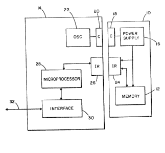
Referring now to FIG. 1, a data storage card is
shown in accordance with the present invention, which
provides a portable and secure means for storing
data. The data storage card, generally referred to
as 10, includes a non-volatile, electrically erasable
memory 12 for the storage of data.
The data storage card 10 interfaces with a
reader/programmer unit 14, for reading and modifying
the data carried in memory 12. The power for the
card electronics and the actual transmission of data
are provided without a direct a physical connection
between the circuitry of the data storage card 10 and
that of the reader/programmer 14. Power for the data
storage card 10 is provided by a high-frequency power
- ~278378
supply 16 which has a secondary coil 18 as its
input, The reader/programmer 14 has a primary coil
20, which is driven by a high-frequency oscillator
22. When the coils 18 and 20 are properly aligned,
and the primary coil 20 is energi~ed hy oscillator
22, a current is induced in the secondary coil 18 and
a regulated voltage is supplied to all card
electronics.
Transfer of data between the data storage card 10
and the reader/programmer 14 is accomplished by
infared optoelectronic devices 24 in the data card 10
and infared optoelectronic devices 26 in the
reader/programmer 14, when properly aligned. Infared
devices 24 and 26 also provide for transmitting and
receiving a clock signal to the memory 12.
When data storage card lO is inserted into
reader/programmer 14, the coils 18 and 20 and the
infared devices 24 and 26 are automatically aligned
for proper functioning.
The reader/programmer contains a microprocessor
28, which initiates data transfers between to and
from memory 12, and transfers the data through a
---- 10 ----
standard RS-232 interface 30 to a host computer on
data I/O bus 32.
Referring now to FIG. 2, the physical forrn of the
data storage card 10 is shown. The data storage card
includes an external case 34, which is completely
sealed and devoid of electrical terminals or
connectors of any kind. The external case 12
measures approximately 3.38 inches in length and 2.12
inches in width, which conforms to the standard ISO
dimensions for financial transaction cards and allows
the data storage card 10 to be easily portable in a
user's pocket or wallet. The card has a thickness of
approximately 0.14 inches, which is somewhat greater
than the standard credit-card dimension.
Included within the external case 34 is a printed
circuit board 36, which provides a mounting surface
for a secondary coil 18, for infared optoelectronic
devices 24 -- which are actually three separate
devices 38, 40, and 42 -- and for all other board
electronics. The secondary coil 18 provides a means
for deriving electrical power for its internal logic
circuity from the reader/programmer 14, when the card
is properly inserted. The IR photodiode 38 is for
~7~33~
providing a clock to the internal logic circuity of
data storage card 10. The IR photodiode 40 and the
IR LED 42 are used for the reception and transmission
of digital data between the internal rnemory lZ of
data card 10 and the reader/programmer 14.
Turning now to FIG. 3, the internal components of
data storage card 10 can be viewed in more detail.
The external case 34 is manufactured from
polysulfone, a rigid high-strength thermoplastic, to
give the data card 10 the properties of rigidity and
long-term durability. This case material serves to
protect the internal components of data card 10 under
conditions of harsh use and in hostile environments.
Moreover, polysulfone has transmissive properties
which are favorable to the passage of infared light
while effectively screening out all visible light.
This property makes it possible to transmit digital
signals in the form of infared pulses, to and from
the data card 10, while keeping the optoelectronic
devices 38, 40, 42 fully sealed and protected within
the external case 34. A suitable polysulfone for
this use is UDEL PSF P-1700 Black 1615, available
from Union Carbide Corporation of Hackensack, N..l.
3~8
The external case 3~ rnay include indici.a molding
into its surface, such as a name, a company loyo, or
any other general identificat:ion information, in any
position other than those occupied by the secondary
coil 16 or the infared optoelectronic devices 38, 40,
22, as indicated in FIG. 1. Such labelling would
also serve to aid a user in orienting the data
storage card 10 with respect to the reader/programmer
18.
The external case 38 is of a clamshell-type
construction having upper and lower halves, as can be
best seen by reference to FIG. 3. The two-piece
external case 12 is manufactured by standard
injection molding techniques and the case halves are
joined at their periphery by screws 44. The
thickness of the external case 34 is limited to .02
inches to ensure proper functioning of the secondary
coil 18 and the infared devices 38, 40, and 42. At
the time of manufacture all voids within the external
case 34 are filled with a standard silicone adhesive
compound, completely sealing the external case 34.
All the internal components of data card lO are
mounted on a non-magnetic printed circuit board 36
-- 13 --
~27~a
made of ~apton, manufactured by 3M-Electronic
Products of St. Paul, r~N. Kapton is a flexible
printed circuit material, approxirnately .007 inc~hes
in thickness, consisting of three layers in its
completed form. A base layer has a copper layer
larninated to it, having the specification of one half
ounce of copper per square foot. Circuit patterns
are screened and etched into the copper layer by
standard printed circuit board fabrication
techniques. A cover layer, prepared with cutouts for
the electronic components, is applied over the copper
etches with adhesive and laminated to form a
one-piece circuit, in which all the thin copper
etches are protected by the cover layer. The
electronic components are then surface mounted on
pads in the etched copper, which extend through
cutouts in the cover layer.
The data storage card ]0 further includes a
secondary coil 18 and a switching power supply 16,
which will be discussed in detail in connection with
FIG. 5 and 6.
The IR optoelectronic devices 38, 40, and 42
should be the tallest components in the external case
-- 14 --
~,~d ~3~
34, so that they touch external case 34 when the
clamshell halves are brought toyether. This will
prevent the silicone adhesive frorn blocking the
emitting or detecting surfaces when it is injected
into the case 34. To achieve this, a srnall layer of
foam 48 is placed below the printed circuit board 36
during assembly, to raise the height of the devices
38, 40, and 42.
Turning now to FIG. 4, the memory 12 and optical
communications circuitry 24 are shown in greater
detail. The memory 12 is a Model X2404 Electrical
Erasable PROM man~factured by Xicor Incorporated of
Milpitas, California. The X2404 holds 4 kilobits,
internally organized as two 256 X 8 pages. The X2404
further includes a serial communications processor
within the chip, providing a bidirectional data
transfer protocol and eliminating the need for any
external memory addressing and control logic.
All data transfers are under the control of
reader/programmer unit 14. The internal serial
communications processor accepts read and write
commands in the form of eight hit words, which
briginate from the microprocessor 28 in the
~ ~7~
reader/programmer unit 14. Single data requests can
initiate the transfer of entire blocks of data,
serially, through bidirectional pin SDA.
The infared optical comrnunications circuitry
consists of IR photodiodes 38 and 40, and IR LED 42,
which eorm an optical communications link with
complimentary and spectrally matched IR devices at
the input to the microprocessor 28 in the
reader/proqrammer unit 14.
The photodiodes 38 and 40 are Model OPL-500
series plastic sensors manufactured by TRW Optron of
Carrollton, Texas. The photodiode 38 receives the
clock from the microprocessor 28 in the
reader/programmer unit 14 and inputs this signal to
pin SCL of memory 12. The photodiode 40 receives
data and read/write commands from the microprocessor
28 and inputs them to bidirectional pin SDA.
Data output on pin SDA is transmitted to the
microprocessor 28 in the reader/programmer unit 14 by
means of the infared L.ED 42, ~Ihich is a series OP140
GaAs Plastic Infared Emitting Diode, spectrally
matched to the OPL-500 sensors, and also manufactured
,
__ 16 -
B~
by TRW Optron of Carrollton, Te~as.
Turning now to FIG. 5, a more detailed vie~,r of
the power circuitry is shown. The high-frequency
oscillator 22, located in the reader/,orograrnmer 14,
utilizes a common 555 timer IC 50 with resistors and
capacitor values chosen to yield an output frequency
of l0 kilohertæ, which is within the standard range
of switching power supplies. A high-frequency
oscillator is desirable in order to minimiæe the
capacitance needed in filtering. The output of the
oscillator 22 is magnetically coupled through primary
coil 20 to secondary coil 18 on the data storage card
l0, inducing a current. In FIG. 5, the single
magnetic core 52 represents the combined function of
two core elements associated with the primary and
secondary coils, which are actually separated by an
air gap, as will be described.
The power supyly circuit 16 on the data storage
card l0 consists of a standard diode-capacitor
half-wave rectifier and a voltage regulator 54. The
voltage regulator S4 is a surface-mounted Model uA723
IC made by Texas Instruments, Incorporated of Dallas,
Texas, with resistor and capacitor values chosen to
-- 17 --
-
33~
yield a regulated output of 5 volts. The output of
the voltage regulator 54 is supplied to the memory 12
and the infared optoelectronic devices 24.
FIG. 6 shows the relationship between the various
magnetic elements which cooperate to effect the
transfer of electric power from the reader/programmer
14 to the data storage card 10. The magnetic core
52, located behind panel 58 of the reader/programmer
14, is a standard EC core made of 3C8 Ferrite,
manufactured by Ferroxcube Corporation of Saugerties,
New York. The magnetic core 52 is wound with sixty
turns of 36 AWG wire (indicated by the reference
numeral 60).
The secondary coil 18 in the data storage card 10
is etched into the copper of the printed circuit
board 36, in the shape of a spiral, and bonded
between layers 62 and 64 of Kapton. The secondary
coil 18 is the equivalent of 70 windings of round 36
AWG wire. The 36 AWG wire has a cross sectional area
of .0000196 square inches. Covering the area behind
primary coil 18, there is a flux carrier 46, which
acts to close the magnetic circuit that is created
when primary coil 20 becomes energized. l'he flux
-- 18 --
3..3~3
carrier 46 is also made of 3C8 ~errite, ~ith a
thickness of approximately .095 inches.
There is a air gap in the magnetic circuit, as
indicated in FIG. 6, between the forward edge of the
magnetic core 52 and the facing edge of the flux
carrier 46. It is desirable for this gap to be .010
inches or less. The 3C8 Ferrite, used for both the
magnetic core 52 and the flux carrier 46, has an
inductance of 75 millihenries per 1000 turns of 36
AGW wire for this air gap range.
When the primary coil 20 is energized by the 10
kilohertz oscillator 22, magnetic flux is created in
magnetic core 52 and travels across the air gap,
through the flux carrier 46, and back to the opposite
Ieg of the magnetic core 52. As the rising and
falling magnetic flux crosses the conductors of
secondary coil 18, an electric current is induced
therein.
Referring now to FIG. 7, the reader/programmer 14
is illustrated in more detail. The reader/programmer
14 is preferably a small, light~/eight, sirnplified
device, which could be mounted unobtrusively in
---- 19 __
various fixed locations, depending on the specific
application of the data storage card 10. In an
access control system to a building, the
reader/programmer ]4 might conveniently be rnounted
beside a door. As a computer security device, the
reader/programmer 14 could be mounted on a computer
console. The size and shape of the reader/programmer
14 also depends somewhat on the specific
application. It is even possible for the
reader/programmer 14 to be incorporated into the
control panel of a larger device, such as a bank
teller machine or a computer keyboard. FIG. 7 shows
the reader/programmer 14 as a free-standing table-top
unit.
The reader/programmer 14 includes a housing 66 to
contain its internal electronics and provide a means
for inserting the data storage card 10 therein. The
housing includes a flat panel 58. The primary coil
20 and the infared optoelectronic devices 26 are
mounted behind the panel 58 in the proper orientation
for interfacing with the data storage card 10.
Data storage card 10 slides down into slots 70,
which provide for proper mechanical al;gnment o~ the
-- 20 --
~ %~7~3
card 10 by holding it ~lat against the panel 58,
preventing it from movinq side to side, and properly
orienting its magnetic and optoelectronic devices
with those of the reader/proyramrner 14.
The reader/programmer 14 may be used with a
keyboard entry device 72. The keyboard entry device
72 includes a keyboard 74 for the entry of personal
identification or verification codes by a user. A
display 76 is included to provide feedback to a user
or to display instructional information. For
displaying data retrieved from the data storage card
10, the keyboard entry device 72 may include an
alphanumeric keyboard and a video display. The exact
form of the keyboard entry device 72 is somewhat
dependent on the particular application of data
storage card 10.
Referring now to FIG. 8, a schematic is
illustrated, showing the microprocessor and
communications circuitry of reader/programmer 14.
As discussed in connection with FIG. L, the
reader~programmer 14 includes a microprocessor 28,
infared optoelectronic devices 26, and an industry
standard RS-232 interface 30.
---- ~ 1 ----
33~
The microprocessor 28 is a Model TMS7742,
manufactured by Texas Instruments, Incorporated of
Dallas, Texas. The TMS7742 is actually an eight-bit
microcontroller chip, containing internal PP~OM
memory. Alternatively, a Model Z8613 may be used,
manufactured by Zilog, Incorporated of Campbell, CA.
The infared optoelectronic devices 26 consist of
two infared LEDs 80 and 82, spectrally matched to
the photodiodes 38 and 40 on data storage card 10.
Infared LED ao supplies the clock to the card 10, and
infared LED 82 is for transmitting data.
Optoelectronic devices 26 also include an infared
photodiode 84 which is matched to the infared LED 42
on the card 10. Infared photodiode 84 is for
receiving~data from the card 10.
The microprocessor 28 communicates with an
external RS-232 device, such as a host computer by
means of an interface driver 78 and an interface
receiver 79. The interface driver 78 and the
interface receiver 79 operate on protocol supplied by
the microprocessor 28. This allows the
reader/programmer 14 to be connected to a variety o~
-- 22 --
~78~
host computers, depending upon the particular
application. The host system ~lill provide the
particular applications software for the
reader/programmer's function. In the case of
security applications, all encryption and decryption
of data is performed in the host computer.
For example, the host computer could command the
microprocessor 28 to activate the infared
optoelectronic devices 26 to request data from the
card memory 12 and transmit that data to the host
computer. The microprocessor 28 turns the infared
LED 80 on and off at a specified clock frequency to
provide the clock to the card memory 12. The
microprocessor 28 sends out a data request command to
the card memory 12 by means of infared LED 82, and
then monitors infared photodiode 84 for the data
being received. When received, the data is sent out
to a host computer by means of the interface driver
78.
To use the data storage card 10 in a security
access application, for example, the user would
approach the security station and insert the card
into the reader/programmer unit 14. The
__ 23 --
microprocessor 28 would be constantly issuing polliny
signals to detect the presence of a card. Upon
receiving a response from the user's card, the
reader/programmer 14 reads a specified memory
location of the memory 12, for a code. The code
references a table of personal identification nurnbers
contained in PROM memory, in microprocessor Z~. The
microprocessor looks up the user's personal
identification code and requests that the user enter
his personal identification code through the keyboard
entry device 72. The microprocessor 28 then cornpares
the personal identification code with the one entered
by the user. If the codes match, the user is given
access; if they don't match, access is denied.
In the application described hereabove, the
user's personal identification code is known only to
the user and is contained only in a look-up table
residing in the reader/programmer 14. Should an
unauthorized person gain access to the data in the
card, the user's personal identification code would
not be revealed, since the card contains only a
pointer to a look-up table. If access is granted by
the reader/programmer 14, additional data could be
accessed from the card -- financial or medical
__ 24 -