Note: Descriptions are shown in the official language in which they were submitted.
3~
-- 1
APPARATUS FOR AND METHOD OF POSITIONIMG
AND SYNCHRONIZING A WRITING L~SER BEAM
Cross-Reference to Relaked Applications:
This application is related to the followiny commonly
assigned, co-pending application: European Patent Publication
Al-0 168 351, published January 15, 1986, and entit].ed IlMETHOD OF,
AND APPARATUS FOR, GENERATING A PREDETERMINED PATTE~N USING LA~ER
RADIATION".
Field of the_Invention:
This invention relates to apparatus for and a method of
positioning and synchronizing a first, writing laser beam with
respect to a workpiece in the illustrative form of a semiconductor
chip. In particular this invention relates to the use of
recognition patterns or entry codes placed in the margin areas of
such a chip, which patterns are scanned by a second, scanning laser
beam, whereby a reflected part of the scanning laser beam is
detected and used to accurately control and synchronize the
relative position of the writing laser beam and the chlp.
~ 2
~ ~W~
Description of The Prior Art:
In European Patent Publication No. 0,088,045,
there is described a method for producing electrically
conductive regions in semiconductor chips, and a
semiconductor structure of high component density which is
produced using this method. During the manufacture of
customized chips, there are used commercially available
silicon disks or wafers which are provided with P- and N-
structures or N- and P-structures at which specific
contact surfaces must be produced. ~hese contact surfaces
connect these structures and depend on the intended
purpose of the chip being produced. There are produced on
the silicon disk or wafer electrically conductive regions
with standard spaces, which are arranged in accordance
with a predetermined raster or grid. Such regions and
standard spaces can be obtained, for example, by applying
an etching or application technique. Depending on the
intended circuit configuration, the conductive region,
which may be composed for example of aluminum and disposed
intermediate these spaces, is directly or indirectly
removed by means of an electron beam or a beam of
electromagnetic radiation. Laser radiation in the form of
a writing laser beam is particularly suited for this
process and the writing laser beam can be positioned and
controlled in a simple manner and serves to irradiate a
photosensitive layer disposed on the disks. During such
processing, the silicon disks or wafers are continuously
displaced relative to the writing laser beam along a
predetermined raster or grid and the writing laser beam is
turned on and turned off by means of a modulator in
accordance with the desired removal geometry. A
~ ~7i~
.~
-- 3
semiconductor structure obtained in accordance with the
aforementioned method comprises in its conductive layer, spaces
which are arranged according to the predetermined raster or grid
and constitute the end points or regions and/or the corner points
or regions of insular conductive regions.
In the above-identified European Patent Publication, a
laser pattern generator and a process for its operation are
described and shown. This laser pattern generator comprises a
laser device for generating a writing laser beam and a laser device
for generating a scanning or reading laser beam. An electronic
system directs the scanning laser beam across the surface of the
chip, and the beam reflection therefrom of an intensity varying in
accordance with the chip surface, is evaluated by at least one
detector. A logic arrangement controls the relative movement of
the writing laser beam and the chip. This process and the
corresponding laser pattern generator will be explained later in
Figures 5a and 5b.
SUM~ARY OF THE INVENTION
It is an object of this invention to provide apparatus
for and a method of positioning and synchronizing the relative
movement of a workpiece in the illustrative form of a semiconductor
chip and a writing laser beam to achieve even more precise chip
component tolerances and to increase the chip processing speed.
3~
--4--
In accordance with these and other objects of
the invention, there is described a semiconductor chip to
be formed by a first writing laser beam directed across a
surface thereof and adapted to use a second scanning laser
beam as is also scanned across the chip surface. The
semiconductor chip has at least two edges intersecting
each other and a recognition pattern disposed on said
surface and comprising a pair of first enter codes
disposed respectively along said first and second edges~
Each of the first enter codes includes a synchronization
mark and a step recognition mark as follows said
synchronization mark, considering that the scanning laser
beams scans from the corresponding edge of the chip across
the synchronization mark and then the step recognition
mark. The first enter codes furnish information for the
evaluation of the scanning laser beam as reflected from
the surface of the semiconductor chip.
In a further aspect of this invention, the
semiconductor chip includes a frame having first and
second frame parts intersecting each other to form a
corner. The frame encloses a logic circuit formed on the
semiconductor chip. There is further included a set of
thread codes respectively disposed substantially
perpendicular to the longitudinal orientation of the first
enter codes respectively. The thread codes are oriented
in a direction toward the frame corner and insure that the
writing laser beam starts in a corresponding corner of the
logic circuit to be formed by the writing laser beam.
~2~7~339~
In a still further object of this invention, a
set of second enter codes is formed respectively within
the frame parts and serves to ensure the precise alignment
of the writing laser beam with respect to the logic
circuit.
In a still further object of this invention, the
set of second enter codes is disposed respectively in an
outer margin zone of each of the frame parts and is
disposed in a substantially parallel relationship wi~h
their respective first enter codes. The set of second
enter codes is disposed in proximity to the core structure
(the so-called gate plane of the semiconductor chip~ and,
therefore, facilitate an optimal fine correction of the
synchronization.
lS In a still further aspect of this invention,
there is disclosed a method of positioning and
synchronizing the relative motion of the writing laser
beam and the semiconductor chipt including the steps of
directing the scanning laser beam from its respective edge
across at least one of the first enter code, the thread
code or the second enter code, detecting the scanning
laser beam as reflected from the surface of said
semiconductor chip, and evaluating the reflected scanning
laser beam to control the relative movement of the
semiconductor chip and the writing laser beam. By so
synchronizing the writing laser beam and the semiconductor
chip, the writing laser beam may be used in accordance
with an "external" indicator pattern to form regions
within said semiconductor chip in accordance with a
corresponding "internal" pattern.
~7~3~
-- 6
With respect to the method of this invention, it is
advantageous for the scanning laser beam to be guided coaxially
with the writing laser beam across the chip surface.
It is also contemplated that the scanniny laser beam be
guided in front of the writing laser beam across the chip surface.
BRIEF DESCRIPTION OF THE DRAWINGS
These and other objec s and advantages of the present
invention will become apparent by referring to the following
detailed description, and accompanying drawings wherein identical
parts have the same reference numerals;
Figure 1 is a diagrammatic view of a corner of a semi-
conductor chip according to this invention having a characteristic
peripheral structure and an outlined core structure;
Figures 2 to ~ are enlarged detail6 II - IV as taken from
Figure l; and
Figures 5a and 5b are diagrammatic representations of the
laser pattern generator, as disclosed in the above identified
European Patent Publication A1-0 168 351, by which the method of
this invention can be implemented to produce the semiconductor chip
as shown in Figure 1.
DESCRIPTION OF THE PREFERRED EMBODIMENT
Referring now to the drawings, Figures 5a and 5b show a
diagrammatic representation of the laser pattern generator as
disclosed in the above identified European Patent Publication A-1-
168 351. By means of this generator, a ----------------------
~ 27'~3~
semiconductor chip 1, as will be described with respect toFigs. 1 to 4, can be processed. There i5 shown a writing
laser beam source A and a scanning laser beam source B,
which are arranged in a horizontal position and with
parallel optical axes. The writing laser beam source A
contains a writing laser device lS, which is followed by a
laser beam switch 16 for turning-off the writing laser
beam 21 in the open condition of the apparatus. An
expander 18 is provided and a pin-hole 16 t iS arranged in
the expander 18. Intermediate the writing laser device 15
and the expander 18, there is positioned a modulator 17 on
the optical axis defined in the writing laser source A.
The expander 18 contains a lens lB'. The entire writing
laser beam source A is mounted in a housing 19. The
modulator 17 and the expander 18 are held in the
aforementioned housing 19 by means of adjustable mounting
or fastening elements 20. The entire housing 19 is also
provided with adjustable mounting or fastening elements 20
which permit the correct arrangement of the optical axis
of the writing laser beam source A.
The scanning laser beam source B i5 mounted in a
housing 22 and contains a scanning laser device 23 from
which a scanning laser beam 23' is directed to an expander
24 of the scanning laser beam source B. This expander 24
also contains a pin-hole 25 in addition to a lens 18'.
Other elements already mentioned hereinbefore in the
description of the writing laser beam source A are also
present in the scanning laser beam source B.
The scanning laser beam 23' emitted by the
scanning laser device 23 is directed into the expander 24.
The members or components of the scanning laser beam
~7~
source B are mounted in a housing 22 which, like the
housing 19 of the writing laser beam source A, can be
correctly positioned by means of adjustable mountiny or
fastening elements 20.
A laser beam collimator C is disposed to
intercept the optical axes of the writing laser beam 21
and of the scanning laser beam 23'. This laser beam
collimator C contains, in a housing 26, a beam splitter 27
for the writing laser beam 21 and a mirrow 28 for the
scanning laser beam 23'. In Figure 5a these elements are
illustrated in top plan view. These elements are
adjustably mounted in the aforementioned housing 26 by
means of adjusting or positioning elements 30. On the
left-hand side of the beam splitter 27 for the writing
laser beam 21, there is located a writing laser beam
detector 29 which controls the correct starting position
of the writing laser beam 21. The reflected writing laser
beam 21 and the reflected scanner laser beam 23' are
coaxially superposed or combined into one beam having a
common optical axis 31, which is directed towards the
arrangement illustrated in Figure 5b.
As shown in Figure 5b, this part of the laser
pattern generator contains a vertically oriented optical
axis as reflected from a beam splitter 32. The common
radiation path 31 of the writing laser beam 21 and of the
scanning laser beam 23' intercepts the beam splitter 32.
A predominant portion of the radiation of the beams 21 and
23' is passed therefrom to a lens 33 of a lens head D and
further to a workpiece G, as may illustratively take the
form of the semiconductor chip 1 as will be described
below in detail. The workpiece G is mounted on a
~7'~39Z
mechanical stage (not shown), which is translated beneath
the vertically disposed optical axis in an X direction at
speeds of up to 300 mm/sec. After each pass of the common
laser beams 21 and 23' in the X direction, the stage is
stepped incrementally in the Y direction. This
accomplishes a raster-like scan of all or part of the
workpiece G. When all the X lines have been scanned, the
workpiece G is rotated by 90 and the scan process begins
anew to provide scan lines in the Y direction. A scanning
laser beam detector 32' is located to follow the beam
splitter 32 for the scanning laser beam 23', in the path
of the composite writing laser beam 21 and the scanning
laser beam 23', which are guided along the common
radiation path 31. It is the purpose of this scanning
laser beam detector 32' to monitor the position of the
radiation path 31.
A lens 33 is provided with an adjusting or
positioning elements 34, which is provided with a piezo-
electric drive 35. Immediately above the lens head D
there is disposed a rotatably mounted turret E. The lens
head D and the turret E form a functional unit or an
optical module F. The turret E comprises a turret
turntable support 36, upon which there are rotatably
located in the presently illustrated example a further
scanning laser beam detector 37, a shearing-interferometer
eyepiece 38 and a microscope eyepiece 39 including a
graticule. For safety reasons, the micro~cope eyepiece 39
is provided with a blocking filter 39' for the writing
laser beam 21. For rea~ons of clarity, the turret E is
shown in Fig. Sb in a developed or diagrammatia form.
3~
--10--
In the aforedescribed illustrated exemplary
embodiment of this inverltion, the writing laser device 15
comprises a naturally air-cooled helium-cadmium laser
system available from Liconix, Sunnyvale, California
94086. Thls laser device 15 comprises a current-
regulating high-voltage power supply, Liconix Model 4200
PS, including cold and warm st~rt-up facilities, time
program and firing control, as well as a laser device
Model 4110B. The main features o~ the writing laser
device 15 are the following: light wavelength 442 nm,
light power (continuous) 10 mW, standard intensity
distribution over the beam diameter, horizontal
polarization direction with deviations of +5%, and the
beam diameter i5 1 . 1 mm.
The scanning laser device 23 may illustratively
comprise a naturally air-cooled Melles-Griot helium-neon
laser system available from ILEE AG, Schlieren,
Switzerland, and which comprises a laser device Model 05-
LHP-lll and a power supply Model 05-LPN-340, 1800 V, 6~5
m~. The light wavelength is 633 nm and the light power i5
1 mWl. The deviation of the beam axis after cold-start i5
smaller than 200 ~Rad and 30 ~Rad after 15 minutes of
operation~ The beam divergence amounts to less than 1.3
mRad and the regulation error of the light power is
smaller than +5%.
The modulator 17 constitutes a naturally air-
cooled, electrically controlled blue laser-light
interrupter system (Coherent Associates, Danbury,
Connecticut 06810) and comprises illustratively a control
device Model 31 and ~ modulator Model 3010. ~he modulator
tube contains a rerigerant crystal of potassium
Z
--ll--
dihydrogenephosphate, which is imbedded in a liquid hsving
the same refractive index and which crystal is provided
with two control electrodes and a photodiode-light meter
attached to the output. The crystal acts in the manner of
a polarization filter, the directional angle of which can
be rotated through a 90 range by applying a voltage of
approximately 600 V.
The expander 18 is composed of two convex lenses
and a pin-hole having a diameter of 10 ~m and arranged at
the common focus of the two convex lenses. The expander 4
increases the diameter and decreases the divergence of the
laser beam according to the expansion ratio, i.e. the
ratio of the focal point distances, and transmits the
image of the light spot within the pin-hole in the output
beam. The expander 18 thus, for example~ removes dark
points which are present in the incoming laser beam and
which, for example~ are due to dust, and also acts to make
the direction of the output beam independent of the
direction of the input beam.
A dichroic beam splitter is used as the beam
splitter 27 for the writing laser beam 21 and comprises a
parallel glass plate with a dielectric metal layer vapor-
deposited upon one side of the glass plate. This dichroic
beam splitter 27 permits the passage of light of a
predetermined wavelength, i.e. of a predetermined color,
in the same direction when such light impinges thereupon
in the throughpass direction. During this passage, the
radiation exit point is offset depending on the refractive
index of the glass for the predetermined wavelength and
depending upon the thickness of the glass plate.
~3 ~7~3~3~
-12-
The piezo-electric drive 35 is a conventional
drive and comprises, in the illustrated example, a Burley
Model PZ70, 1000 V power supply and a ~urley Model PZ40
piezo translator. The piezo crystal stack contained
therein expands approximately proportional to the voltage
applied thereto and displaces thereby the lens 33 along
its horizontal axis.
The microscope contains the lens 33 and the
microscope eyepiece 39. This lens 33 comprises a convex
lens system with or without a standard cover glass on the
working side thereof and focuses the concentrically and
parallely entering blue and red laser beams to form the
smallest possible focal spot at the working distance. The
lens 33 furthermore passes an enlarged virtual image of
the green-colored illuminated image field extending
concentrically with respect to the focal spot and which
can be viewed by means of the microscope eyepiece 39. The
microscope converts the mechanical displacement by means
of the piezo-electric drive 35 into a displacement of the
center of the image field and of the center of the focal
spot. Thus, the required adjustments in the Z direction
may be carried out by an amount delta Z, and in a Y
direction may be carried out by an amount delta YO The
extent of the delta æ is indicated by an arrow in Fig. 5b,
noting that the shift of delta Y would be orthogonal with
respect thereto.
The microscope eyepiece 39 is constructed as a
convex lens system and funstions as a magnifying lens to
provide a magnified visible image from the virtual image
produced by the l-ens 33.
3~
- 13 -
The shearing-inter-ferometer contains a mirrow which can
be placed into the radiation path, the parallel glass plate, and
the eyepiece 38. This unit constitutes the sh~ariny-interferome'cer
for measuring the deviation of the distance of the reflectiny
aluminum surface from the focal plane of the lens 33.
The writing laser beam detector 29 and the scanning laser
beam detectors 32' and 37 preferably are each comprised of a
central of inner, relativsly insensitive and an external, more
sensitive arrangement of silicon photodiodes. By means of the
aforementioned detectors there is determined, on the basis of the
laser beam reflected from the workpiece G or on the basls of a
laser beam obtained in any other suitable manner, whether the
related laser beam is located in the correct position or is spaced
in a certain direction from this corre¢t position. The output
signals generated by the detectors 29, 32' and 37 are evaluated in
order to determine the relative positions of the workpiece G and
the writing laser beam 21 and to possibly correct the relative
movements of the workpiece G and the writing base beam 21 such as
to write a predetermined pattern.
In the semiconductor chip 1 as will be described below
with respect to Figures 1 to 4, a metalized raster serves as a
reference structure. That metalized raster is further shown and
described in the above-identified European Patent Publication Al-
0 168 351 as a metalized grid disposed upon the surface or regions
of the chip 1 and including a firs-t set of evenly spaced,
horizontally disposed metal strips, e.g. aluminum, and a second set
of evenly spaced metal strips disposed vertically and substantially
~.~Y~3~
-14-
perpendicular to the strips of the first set. AS shown in
Figure 5b, the writing laser beam 21 and the scanning
laser beam 23' are focused along path 31 and are directed
by the divider 32 vertically to be focused by the lens 33
as a beam spot on the surface of the workpiece wafer G,
e.g. the chip l. The spacing between adjacent strips of
the grid amounts to, for example, about 7 ~m and their
width to, for example, about 5 ~m. In such an embodiment
of the chip l, the writing laser device 15 may be, for
example, an argon-ion laser having a power in the range of
about 1 to about 5 mW at a wavelength of 458 nm and such
laser can be obtained, for example, from Spectra Physics,
Mountain View, California, Model 162A.07, or from American
Laser Corporation, Salt Lake City, Utah, Model 60C. The
writing laser device 15 also may be, for example, a
helium-cadmium laser having a power in the range Gf about
7 to about 40 mW at a wavelength of 442 nm or a power in
the range of about 1 to about 10 nW at a wavelength of 325
nm. Such laser devices are respectively available and
Model 4200 N and Model 4200 NB from ~iconix, Sunnyvale,
California.
The switching of the continuous laser power is
effected by an electro-optical modulator or beam switch
17, for example, Model 3010 produced by Coherent Inc.,
Modulator Division, Palo Alto, California. The modulator
17 may also constitute an acousto-optical modulator or
beam switch, for example, Model 304D produced by the
Modulator Division of Coherent Inc. The required
switching time is determined by the writing rate and by
the local resolution and, for example, may amount to about
2 ~s. The sub~equent beam expander 18 increases the
diameter of the laser beam 21, for example, tenfold. The
3 ~3'~
- 15 -
horizontal writing beam 21 is deflected in a vertical direction by
means of the deflection mirror 32. In this example, 'che lens 33
has a focal length of 18 mm and a diameter of 10 mm. The resul-ting
spot size is about 2 micrometers and the depth of field is about 13
micrometers. The deflection mirrow 27 may he arranyed to be
controllable or adjustable. The scanning laser device 23 in this
e~ample is a He-Ne laser of an output of 1 mw and a beam diameter
of 0.65 mm. By means of the expander 2~, the scanning l~ser beam
23' is enlarged 4 times and is superimposed on the writing laser
beam 21 by means of the adjustable deflection mirror 28.
The laser pattern generator, as described above with
respect to Fiyures 5a and 5b, is used to scan its composite laser
beam across the surface of the workpiece G in the illustrative form
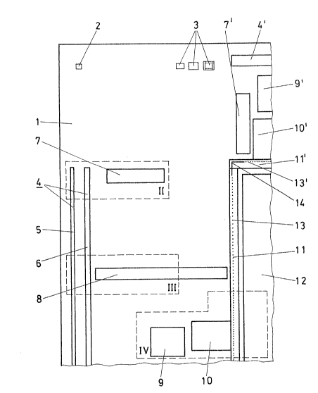
of the semiconductor chip 1, as will now be described. Figure 1
shows the chip 1, on the surface of which an adjusting structure 2
and several adjusting elements 3 are disposed. The elements shown
on the chip 1 reflect the scanning laser beam 23' (Figures 5a and
5b) with varying intensity. Along a first edge of the chip 1 as
oriented vertically as shown in Figure 1, a first enter code 4 is
located. In the upper, right hand corner as shown in ~igure 1, a
part of another first enter code 4' is shown that extends in
parallel with a second edge of the chip 1 as disposed horizontally.
The first enter code 4 is composed of two structures that extend
in parallel with each other, namely a synchronization mark 5 and of
a step recognition mark 6. The objectives of these marks 5 and 6
are indicated by their names and are used to provide synchronizing
and recognition signals ~
3~
- 16 -
Perpendicular to the vertical orientation of the first enter code
4, a thread code 7 extends in a direction towards a corner 14 of a
frame as comprised of frame part 11 and frame part 11'. The frame
encircles a logic circuit 12 to produce by the above-descrihed
pattern generator. Another thread code 7' extends perpendicular to
the other, horizontally oriented enter code 4'. An active field 8
extends also perpendicular to the first enter code 4, the active
field 8 usually being generated in block raster font and
illustratively containing the name of the client and perhaps the
type of logic circuit to be produced. In the lower part of Figure
1, a first line circuit - PAD -g is located, while in the upper
right-hand corner a second line circuit g' is disposed.
Corresponding input and output structures 10 and 10' are connected
with the first line circuits 9 and 9', these structures naturally
being connectsd to the frame parts 11 and 11'. In these frame
parts ll and 11', a second code 13 is located that extends in
parallel to the first enter code 4, and another, second enter code
13' is located in parallel with the okher first enter code 4'.
Figure 2 shows the detail II of the chip 1 from Figure 1.
This enlarged detail contains the upper part of the first enter
code 4 with its synchronization mark 5 and its step recognition
mark 6 and the top view of the thread code 7. The first enter code
4 supplies the processing information, and the thread code 7 guides
the composite scanning laser beam 23' and writing laser beam 21
along in the precise path to the start o~ the logic circuit 12 to
3~
-17-
be manufactured. The first enter codes 4 and 4' are used
as the laser beams 21 and 23' scan the chip 1 in
horizontal and vertically disposed rasters as explained
above to produce the required synchronizing and
recognition signals, whereby the relative movement between
the chip 1 and the composite beams 21 and 23' may be
controlled.
Figure 3 shows two other cutouts of the
synchronization mark 5 and of the step recognition mark 6.
In this connection, a part of the active field 8 is shown
in diagrammatic form. The objective of the active field 8
was described above.
The enlarged details according to Figure 4 show
the peripheral structure (PAD-field - the first line
circuit 9) and, on the right-hand side, the core structure
with its gate field 12 (logic). Diagrammatic
representations are shown of the line circuit ~ and of the
related input and output ~tructure 10. This input and
output structure lO is connected to the frame part ll and
is also connected electrically with the logic circuit 12
located within the frame part ll. At the margin of the
frame part ll, the second enter code 13 is located.
Thus, it is seen that the semiconductor chip l
as disclosed in Figures 1 to 4 is processed by the laser
pattern generator as shown in Figures 5a and 5b. In
particular, the writing laser beam 21 and the scanning
laser beam 23' are directed along the axis beam path 31 as
a composite beam and are thereby reflected by the divider
32, and focused by the lens 33 onto the workpiece wafer G
in the form of the semiconductor chip l. The scanning
laser beam 23' is reflected from the surface of the
~ ~t7~
semiconductor chip 1 and is detected by at least the detector 37 to
be evaluated, whereby the relative movement of the semiconductor
chip 1 and the writing laser beam 21 may be accurately controlled.
Though three different types of codes or reference marks 5, 6 or 7
are shown, it is contemplated that it may nok be always necessary
to use each of these reference marks to achieve the desire~
coordination between the relative movement of the writing laser
beam 21 and the semiconductor chip 1. The laser pattern yenerator
as shown in Figures 5a and 5b is computer controlled and includes
a memory in which various patterns are stored and are used to
control the pattern or topography of the logic circuit 12 as formed
by the writing laser beam 21.
The placement of the recognition patterns on the semi-
conductor chip 1 in advance of the logic circuitry 12 to be formed
by the writing laser beam 21 insures additional time for the laser
pattern generator to respond to the reflected scanning laser beam
and to control the relative movement of the writing laser beam 21
and the semiconductor chip 1. In addition, the scanning and the
"etching" or "denuding" effected by the writing laser beam 21 may
~0 be carried out more precisely, whereby the topography of the logic
circuitry 12 formed in the semiconductor chip 1 may be more
precisely formed. Thus, the method and semiconductor chip of this
invention are
z
--19--
particularly suited for the manufacture of large numbers,
as well as relatively small batches of the semiconductor
chips lo
In considering this invention, it should be
remembered that the present disclosure is illustrative
only and the scope of the invention should be determined
by the appended claims. For example, the laser devices of
this invention may be arranged in different orientations
than that illustrated in the attached drawings, and the
optical paths of the scanning laser and the writing laser
beams may be rearranged.