Note: Descriptions are shown in the official language in which they were submitted.
MULTI-CHANNEL MODULATED NUMERICAL
FREQUENCY SYNTHESIZER
Backqround of the Invention
The present invention relates generally to a
multi-channel signal synthcsizer system providing a wide
variety of complex signal waveforms, and, more
particularly, relates to a four channel numerical
digital synthesizer system providing one or more output
signals having selectable waveform and modulation
characteristics.
Most signal synthesizer systems provide precision
waveforms, signals with frequency accuracy and
resolution for test evaluation of electrical systems.
For example, a signal channel synthesizer system can be
synthesizer, function generator and sweep generator
providing sine waves, square, triangle and ramp
waveforms for use. As a synthesizer, the single channel
system provides waveforms having precise frequency
control. As a function generator, the synthesizer
system provides a variety of waveforms including sine,
square, triangle and ramp. As a sweep generator, the
synthesizer can sweep over a range of frequencies.
However, there is a high demand for much improved
performance of the prior art synthesizer systems in
spectro purity, phase noise and phase accuracy. Further
more, it is desirable to provide the prior art
synthesizer system with a variety of additional
capabilities and functions.
Various types of digital frequency synthesizers
are known in the art. U.S. Patent 3,375,269 entitled
"Digital Frequency Synthesizer" granted to Leland B.
Jackson on May 22, 1973, discloses a digital frequency
synthesizer which is programmable to provide desired
frequency outputs. Jackson discloses a digital
synthesizer which includes storage means such as a read- -
only-memory (ROM) in which digital values corresponding
to digital samples of the desired output signal from the
synthesizer are stored. These digital samples represent
a predetermined waveform, such as a sine wave. In
Case 186194
1~'78~ '3
response to a digital signal representing a
predetermined frequency output the storage means
provides output signals corresponding to the digital
values stored therein. The successively generated
digital values are fed to a digital-to-analog convertor
(DAC) which generates a step-type repre entation of the
desired output signal. The output signal is then
smoothed in a low pass filter to provide an output
signal having the predetermined frequency and waveform.
The synthesizer system of Jackson does not provide
multi-channel capabilities nor does it provide selective
modulation and waveform generation capabilities.
An object of an aspect of the present invention is
to provide a multifunction digital frequency synthesizer
which is easily programmable to provide complex output
waveform signals from a variety of selectable
fundamental waveforms.
An object of an aspect of the present invention is
to provide such a multifunction digital frequency
synthesizer system having multiple internal channels to
provide frequency, amplitude, phase and pulse modulation
of a single channel with selectable waveform or be
summed at the output provide a single complex output
waveform.
An object of an aspect of the present invention is
to provide such a digital frequency synthesizer which
utilizes a single VLSI integrated circuit (IC) to
achieve the direct digital synthesis, waveform
generation, summation, multiplication and multiplexing
functions to achieve a high level integration which
results in an output signal having well-defined accuracy
and exact repeatability at a low cost.
SummarY of the Inventio~
An aspect of the invention is as follows:
A digital frequency synthesizer comprising:
frequency input means for setting a predetermined
~'7
3a
output frequency and for generating fir~t digi~al
signals representing said predetermined output
frequency;
frequency modulation input means for inputting a
frequency modulation signal;
waveform selection input means for generating a
waveform selection signal for selecting a predetermined
output waveform;
first summing means coupled to said frequency
input means and said frequency modulation input means
for summing said first digital signals and said
frequency modulation signal and generating second
digital signals representing said predetermined output
frequency modulated by said frequency modulation signal;
phase accumulator means coupled to said first
summing means for receiving said second digital signals
and responsive to a first clock signal for generating a
cyclic progression of digital binary numbers
representative of an output signal having said0 predetermined output frequency;
phase modulation input means for inputting a phase
modulation signal;
second summing means coupled to said phase
modulation input means and to said phase accumulator5 means for summing said phase modulation signal with said
digital binary numbers output by said phase accumulator
means and outputting third digital signals
representative of said digital binary numbers modulated
by said phase modulation signal; and
waveform generation means coupled to said waveform
selection input means and to said second summing means
for generating a plurality of selectable waveforms and
responsive to said third digital signals and to a
control signal for generating digital output signals5 representative of said selected waveform modulated by
3b
said frequency modulation signal and sald phase
modulation signal and having said predetermined output
frequency.
In accordance with the principles of the present
invention a multifunction digital frequency synthesizer
includes an input device such as a keyboard with display
and a communication bus interface for programming a
1~ 7~
pre~etermlned output frequency and other characteri~tics
of a desire~ output signal and for generating digital
signals repxesenting the programmed inputs. A waveform
synthesis circuit utilizes digital techniques to
calculate numerical representations of complex
waveforms. The waveform synthesizer can ~enerate a
variety of selectable waveforms on four independent
internal channels. Any combination of the generated
waveforms on the internal channels can then be used to
modulate one of the channels in amplitude, phase,
frequency, or pulse modulation. Any combination of
modulation type and waveform source may be used
concurrently. For example, the sum of the waveforms on
channels B and c may be utilized to amplitude modulate
the waveform on channel A while simultaneously the
waveform on channel D frequency modulates the waveform
on channel A. Further any of the waveforms on the
independent channels may be summed together to provide a
complex waveform at the output.
The multiple waveform generation, multiple
waveform summation and complex waveform modulation is
achieved by the use of time multiplexing. This use of
time multiplexing results in a chip design that requires
much less active area on the integrated circuit chip.
The waveform synthesizer provides four fundamental
waveform signal types including sine, square, ramp,
triangle waves and both uniform noise and Gaussian noise
plus a DC reference. A phase accumulator generates a
digital ramp signal from which the triangle and ramp
waveforms are generated by a simple numerical conversion
process. A storage means such as a ROM stores a
plurality of digital values corresponding to the
magnitude of a sine wave at a plurality of phase points.
The digital ramp output of the phase accumulator
correspond to these phase points. To generate a sine
wave the storage means in response to the phase
accumulator output signal provides digital output values
representing of the desired sine wave output signal. A
Case 186194
1~ 7~
noi~e generator in com~ination with a noise ROM
provides both uniform noise and Gaussian noise si~nals.
The square wave is diyitally synthesized by outputting a
series of digital ones and switching the level at the
desired times. The various output waveforms from the
waveform synthesizer are coupled to a multiplexer where
the desired output waveform for each of the four
internal channels is multiplexed onto a single output
line. The four time-multiplexed internal channels may
then be combined in a summer in any serial combination
to provide four time-multiplexed signals. The four
signals are coupled to an input multiplexer for
modulation of internal channel A and a selected one of
the signals is also coupled to a DAC and a low pass
filter to provide a smooth output signal having the
desired frequency modulation and waveform.
Up to three output sections may be added to
provide a system having up to four output signals for
which frequency, amplitude, waveform and phase can be
independently set for each of the output signals.
Although the output signals in this option are
independent, the relative phasa between the outputs can
be precisely controlled from 0 degrees to 359.9 degrees
with a resolution of 0.1 degrees.
The utilization of time multiplexing allows
substantial reduction of the hardware required for the
waveform synthesizer, the summation circuitry and the
multiplication circuitry. For example, in the case of
the waveform synthesizer the active hardware required is
reduced by a factor of approximately four while still
providing four internal channels. This hardware
reduction allows all of the above described capabilities
to be provided in one IC chip. The single IC chip
provides the desired feature set with lower cost,
greater reliability and improved ease of application
compared to the prior art synthesizers. In addition,
direct digital synthesizers insure accUracy and exact
repeatability. Compared with analog technology drift is
Case 186194
8~jO~
eliminated, accuracy is improved and the number of
required adjustments is greatly reduced.
,Brief Description of the Drawinas
Figure 1 is a block diagram illustrating a
conceptual representation of a digital frequency
synthesizer system according to the principles of the
present invention.
Figure 2 is a basic schematic block diagram of a
preferred embodiment according to the principles of the
present invention.
Figure 3 is a simplified block diagram of the
digital signal processor of Figure 2.
Figure 4 is a simplified block diagram of a four
channel implementation of the digital signal processor
of Figure 3.
Figure 5 is a detailed block diagram of the
waveform generator utilized in the digital signal
processor of Figure 3.
Figure 6 is an analog representation of the
digital signals utilized to digitally synthesize the
sine wave output signal.
Figure 7 is an analog representation of the
digital waveforms digitally synthesized by the waveform
generator of Figure 5.
Detail Descri~tion of the Preferred Embodiment
Referring now to Figure 1, a conceptual block
diagram of a multifunction digital frequency synthesizer
according to the principles of the present invention is
shown~ The synthesizer comprises four essentially
identical synthesizer channels 10, 20, 30 and 40,
channel A, channel B, channel C and channel D,
respectively, and provides a single output at the
output channel 23. Channel A is the primary synthesizer
channel 10 comprising an adjustable frequency generator
101 coupled to a phase offset and modulation block 103
which in turn is coupled to a waveform generator 107.
Case 186194
1~7~)9
Waveform generator 107 digitally synthesizes precise
sine, square, triangle, ramp, uniform noise, Gaussian
noise and DC waveforms. Any one of these fundamental
waveforms may be selected and oUtput to amplitude
modulation block 105. The output of ampl itude
modulation block 105 is coupled to the channel summer
block 21 via pulse modulation block 19. The desired
output frequency for frequency generator 101 is set by
an input signal on line 25. The initial phase angle and
lo amplitude level for channel A may also be set by inputs
on lines 27 and 29 respectfully.
Channels B, c and D comprise essentially
identical synthesizer blocks 20, 30 and 40,
respectfully. Each channel synthesizer 20, 30 and 40
comprises an adjustable frequency generator 201 coupled
to phase offset adjustment 203 and then to waveform
generation block 207. In a manner similar to waveform
generation block 107 six fundamental waveforms are
digitally synthesized and a selected one is output to
amplitude level set block 205. The desired freguency,
phase angle offset, waveform and amplitude level are set
independently for each of the channel synthesizers 20,
30 and 40. ~he output of each channel synthesizer 20,
30 and 40 may be selectively coupled to one of several
summing blocks 11, 13, 15, 17 and 21. FM summing block
11 may have any combination of the outputs of the
channel synthesizers 20, 30 and 40 input to it and
provides a FM signal to the channel A frequency
generator 101. Similarly the phase modulation summing
block 13, amplitude modulation summing block 15 and
pulse summing block 17 may sum in any combination one or
all of the outputs of the channel synthesizers 20, 30
and 40 to provide modulation signals to phase modulation
block 103 amplitude modulation block 105 and pulse
3~ modulation block 19, respectively. In addition one or
more of the channel synthesizers 20, 30 and 40 outputs
may be coupled to the channel summer 21 to be summed
with the output of the pulse modulation block 19 and
Case 186194
1~78~,()'~
with each other to provide the output on the output
channel 23.
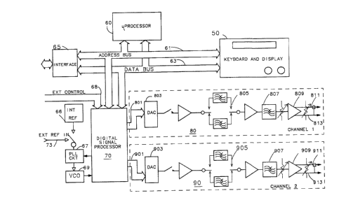
Referring now also to Figure 2, a schematic block
diayram of the multifunction digital frequency
synthesizer described her2inabove is shown. The ~igital
frequency synthesizer system comprises a keyboard and
display unit 50, a host microprocessor 60, a digital
signal processor 70, communications bus interface 65 and
output channel boards 80 and so providing output
lo channels 1 and 2, respectully. The keyboard and
display unit 50 provides a keypad and a backlit liquid
crystal display providing the capability to completely
program all parameters of the output signals on channel
1 and channel 2. Programmable parameters include
selectable waveforms, phase offsets, frequencies, fine
level settings and modulation types. Softkeys (not
shown) provide complete control of operating modes and
sequence functions. The keyboard and display unit 50
also provides precise control of the relative phase
difference between the independent outputs on channels 1
and 2. Microprocessor 60 provides overall control of
the synthesizer system (a microprocessor designated
MC6809 manufactured by Motorola may be used for this
application). Microprocessor 60 also includes required
random-access-memory (RAM) and ROM space for storing
various sèts of numerical data representing fundamental
waveforms used by the synthesizer system. The
communication bus interface 65 allows the digital
frequency synthesizer system to be networked with other
instruments to provide additional testing and analysis
capabilities. The digital signal processor 70
comprises an integrated circuit providing direct
numerical digital synthesis, summation, multiplication
and multiplexing capabilities to provide for multiple
independent synthesizer channels as shown in Figure 1.
In the preferred embodiment, a digital signal processor
70 comprises a single monolithic integrated circuit
utilizing NMOS VLSI technology. The internal
Case 186194
1~78~ '3
reference ~6, phase lock loop 67 and the voltage-
controlled oscillator 69 provide the digital processor
70 with the necessary reference and clock signals.
External reference signals may be input on line 73 to
provide the capability to phase lock the system to an
outside source (not shown). External control signals on
bus 68 provides the capability to directly program
internal channel A to provide a predetermined sequence
of output signals having independent phase, amplitude
and frequency states. Output channel boards 80 and 9o
provide two identical output channels, channel 1 and
channel 2, respectfully. Output channel board 80
receives the output signal from digital signal
processor 70 on signal bus 801. The output signal from
the digital processor 70 is in the form of a 12-bit
digital word representing the desired output signal for
output channel 1 which is programmed at the keyboard and
display unit 50. The DAC 803 converts the digital
signal to an analog waveform. Analog filters 805 and
807 provides smoothing while differential amplifier 809
provides a differential output on output lines 811 and
813. In a similar manner output channel board 90
provides a differential analog output on lines 911 and
913.
Referring now to Figure 3, a simplified block
diagram of the basic signal generation circuitry is
shown. The key component of the signal generation
circuitry is the phase accumulator 75 which provides a
cyclic progression of binary numbers on its output line
751. The sequence of binary numbers output on line 751
is passed through a waveform generating circuit 81 to
provide various selectable periodic waveforms. Adders
77 and 79 provide frequency and phase modulation of the
output of the accumulator 75. The base frequency of the
output signal is set on line 72 at the input adder 77.
A frequency modulation signal on line 74 provides
frequency modulation of the output signal by varying the
slope of the ramp at the output 751 of the accumulator
Case 186194
~;~78~
75. An input signal on line 76 may be utilized to
provide an initial phase offset and/or continuous phase
modulation of the output signal from the accumulator 75.
A multiplier 83 receives control signals on line 78 to
adjust the overall amplitude of the waveform and also to
provide amplitude modulation of the output waveform.
Multiplier 83 also provides pulse modulation of internal
channel A. As implemented, pulse modulation is a
special case of amplitude modulation.
Referring now to Figure 4, a simplified block
diagram of the four-channel implementation of the basic
circuit 71 of Figure 3 is shown. Multiplexer 85 is
divided into four input multiplexers 851, 853, 855 and
857 to provide four independent internal synthesizer
channels. Four-channel operation is achieved when
control logic circuitry 87 selects a different
multiplexer input on successive clock cycles thereby
representing a different operating poin~ fox each signal
parameter to the basic circuit 71. The result at the
output 751 of the accumulator 75 is a progression of
four internal separate binary number patterns
multiplexed in time, each representing a separate
internal channel. The parameters of amplitude level,
phase offset, frequency and waveform type may be set for
each of the independent channels. Thus at the output 82
of the multiplier 83, four independent time-multiplexed
signals corresponding to internal channels A, B, C and D
are output, each signal having predetermined frequency,
phase, waveform and amplitude level. In addition,
channel A may be modulated by any combination of
channels B, C and D. Serial adder 84 comprises an
accumulator that either passes the signals through
unmodified or that sums any serial combination of the
four internal channels. The serial adder 84 is coupled
to demulitplexer 86 where a selected internal channel is
demultiplexed onto the output line 861 for output
channel 1. Up to four demultiplexers 86 may be utilized
in parallel to provide up to fGur output channels having
Case 186194
1 ~ 7~
any selected one of the four multiplexed oUtput signals
from serial adder 84 demultiplexed on each of the four
output channels (in Fiyure 4, output charlnels 1 a~d 2
correspond to output buses 801 and 901, respectively, as
shown in Figure 2). Modulation ~eedback line 93 couples
the outputs of the serial adder 84 to multiplexer 851
via control logic 87 to provide modulation signals for
internal channel A.
RAM 89 stores selectable values of phase offset,
o amplitud~ and frequency and is directly accessed by
external control signals on bus 68 to program internal
channel A to provide a predetermined sequence of output
signals having independent phase, amplitude and
frequency states. Up to sixteen
frequency/amplitude/phase states can be entered into the
RAM 89 from the keyboard and display unit 50. To shift
or "hop" between states, an external device (not shown)
addresses the four-bit TTL-level external control bus
68. As the address coupled to the bus 68 varies, the
internal channel A signal will shift to the
frequency/amplitude/phase state that corresponds to that
address of the RAM 89. Phase continuous frequency
shifting can be done very quickly since the signals are
digitally synthesized and there is no settling time as
in analog phase lock loop synthesizers. The other
internal channels B, C and D may be used to modulate
internal channel A while channel A is shifting. For
example, internal channel B could be programmed to
modulate internal channel A with uniform noise while
channel A is shifting. This would provide an output
signal on output channel 1 (line 861) having controlled
amounts of phase noise added to the shifting signal.
The digital signal processor 70 comprises the
simplified block diagram shown in Figure 4. The digital
signal processor 70 is a fully digital approach to the
analog functions of modulation and signal generation
implemented in a signal chip. The data path
architecture of the digital processor 70 comprises 26
Case 186194
1;~78~i()t~
pipe stages in which 23 simultaneous operations take
place. To achieve an increase in speed of the circuit
extensive hard-coding was utilized. Extensive use of
multiplexing circuits allowed- a large reduction in
circuit compsnents and required chip space.
Referring now to Figure 5, a more detailed block
diagram of the waveform generator 81 is shown. The
waveform generating or shaping circuit digitally
synthesizes four fundamental waveforms including ramp
wave, square wave, triangle wave and sine wave plus
uniform noise, Gaussian noise and a DC output. The ramp
waveform on line 823 is derived directly from the binary
number sequence on line 791 at the output of the phase
adder 79. The complementor block 841 is a programmable
invertor to invert the ramp up signal to provide a ramp
down signal. The triangle waveform on line 821 is also
derived directly from the input on line 791. ROM 819
stores digital values corresponding to the magnitude of
digital samples representing the first quadrant of a
sine wave. The binary numbers input on line 791
represent address signals corresponding to the storage
location in ROM 819 where the digital value associated
with the phase of the sign wave corresponding to the
associated address signal is stored. Complementor
circuit 817 is a programmable invertor that accesses ROM
819 as a function of the quadrant of the sine wave. ROM
819 provides output signals on line 825 which represent
two quadrants of the sine wave. A square wave
synthesizer 839 outputs a sequence of binary ones to
provide a steady DC level. To achieve a square wave,
the steady DC level is shifted by the sign generation
logic 847 to provide a square wave having the
predetermined frequency. The noise generator 835 is a
31 bit linear feedback shift register which provides 128
seconds of pseudorandom, uniformally distributed
cyclic noise to provide a uniform noise signal output on
line 829. A Gaussian distribution of noise amplitudes
is derived by filtering the uniform noise from the noise
Case 186194
1 ~ 7 ~
generator 835 through a noise ROM 837 to provide a
Gaussian noise signal on line 831. Multiplexer 845, in
response to control signals on line 833, matches a
predetermined waveform to the corresponding internal
channel A, B, C or D and couples each internal channel
signal on line 815 multiplexed in time to the sign
generation logic 847. The multiplexed output of the
sign generation logic 847 then is then coupled to the
serial adder 84 via multiplier 83 (as shown in Figures 3
and 4).
Referring now also to Figures 6 and 7, the input
signal on line 791 is a 14-bit digital signal
represented by analog ramp signal 601. Bits 0-12
represented by analog waveforms 605 and 607 are
complemented by bit 13 (represented by analog waveform
603) in complementor 841 to synthesize the ramp waveform
on line B23. Bits 0-11, waveform 607, are complemented
by bit 12, waveform 605, in complementor 817 to
synthesize a digital triangle waveform on line 821.
Bits 0-11, waveform 611, address the sine ROM 819 which
outputs the digital valves corresponding to the phase
points represented by Bits 0-11 to synthesize the first
quadrant 611 of the sine wave halves 609. Bit 12,
waveform 607, complements Bits 1-11 to reverse the order
in which sine ROM 819 is addressed to produce the second
quadrant 613 of sine wave 609. When bit 12, 605, is
low, the first quadrant 611 is output by sine ROM 819
and when bit 12, 605, is high, the second quadrant 613
is output by sine ROM 819.
Bit 13, waveform 603, is also coupled to the sign
logic circuits 847 which performs the final step in the
waveform synthesis. For example, when one or more of
the four internal channels A, B, C and D are programmed
to have a sine waveform, control signals on line 833 to
multiplexer 845 cause the sine wave halves, waveform
609, to be multiplexed onto line 815 in the time window
corresponding to whichever channel is to be a sine
wave. The sine wave halves, waveform 609, is coupled to
Case 18619~
1~7~tjU~3
14
the sign logic circuit 847. When bit 13 is low, the
sign logic circuit outputs on line 851 the positive
half, quadrants 611 and 613, of the sine wave. When bit
13 goes high, the sign logic circuit reverses the
polarity of sine wave half 615 to output a digital
signal on line 851 which represents a complete sine wave
as illustrated by waveform 707. In a similar manner,
the sign logic circuit 847 reverses the polarity (level)
of the digital signals input on line 815 to provide the
selected waveform. Four basic waveforms, ramp 703,
triangle 705, sine 707 and s~uare 709 and uniform noise
and Gaussian noise 713 plus a DC level (not shown) may
be output on line 851.
Case 186194