Note: Descriptions are shown in the official language in which they were submitted.
87~8
DEVICE FABRICATION THROUGH ETC~ING A SUBSTRATE WITH
PLASMA CONFINED ~O SUBSTRATE AREA
Background of the Invention
1. Fleld of the Invention
This inventior. relates to device processing.
2. Art Background
The etching of a first materia] without
unacceptably removing or damaging a second is often
required in processes such as semiconductor device
fabrication procedures. For example, it is desirable in
certain situations, such as in the production of
appropriately configured gates, to remove a region of
silicon and/or metal silicide without causing unacceptable
removal of an underlying or adjacent region of a silicon
oxide, e.g., silicon dioxide. Processes such as plasma
etching and reactive ion etching employing a chlorine-
containing gas are often utilized to accomplish these
results. In these techni~ues, a chlorine-containing gas is
typically introduced in proximity to the body to be etched,
and a plasma is established in the gaseous medium by
applying r.f. power between electrodes. Typically, the
substrate rests on the powered electrode, and the DC
electric field associated with this electrode directs the
energetic entities produced in the plasma (e.g., ionized
molecular fragments, ionized molecules, and ionized atoms)
towards the substrate and, through various mechanisms,
causes removal of the impacted material.
A variety of etching apparatus geometries and
processing conditions has been employed in the dry etching
of materials such as silicon. The specific configuration
and etching conditions are generally chosen to yield
etching characteristics tailored to the particular
semiconductor device fabrication application. For example,
a hex reactor, e.g., an apparatus disclosed in U. S.
Patent 4,298,443, issued November 3, 1981 and illustrated
in the Figures of that patent, is capable of ~rocessing a
large number of substrates during one etching procedure.
1~78768
- 2 -
This reactor includes a hexagonally shaped cathode
contacting the substrates and typically a grounded outer
shell that functions as the second electrode. A plurality
of substrates is positioned on each face of the hexagonal
cathode. Thus, for example, if 4 substrates are placed on
each face, it is possible to process 24 substrates during
one etching procedure. Alternatively, parallel plate
reactors, i.e., reactors having a cathode and anode each
formed by a plate whose major surfaces are held in a
parallel configuration, have been advantageously employed
in less demanding applications to provide suitable
simultaneous etching of 4 to 6 substrates. In a third type
of reactor, one substrate covers essentially the entire
r.f. driven electrode, and a second electrode, e.g., a
parallel plate or vessel component, is provided.
While in many situations etching involving
plasma-generated energetic entities is advantageously
employed, lt is not without associated difficulties. For
example, the use of a plasma often leads to the deposition
of contaminating materia]s on the substrate surface. These
contaminating materials such as metals from the reaction
vessel or substrate holder, e.g., aluminum, either degrade
device properties or hlnder ~ubsequent processing
procedures. Various measures ha~e been employed to avoid
such contamination. For example, in the case of a hex
reactor, a tray surfaced with a material, e.g., a polymer
such as a polyarylate, is positioned on each face of the
hex cathode with openings through which the substrates are
inserted. Thus, the substrates contact the underlying
electrode while remaining exposed to the plasma
environment.
Although as presently practiced, dry etching
yields excellent results with limited shortcomings, new
applications have produced further, yet unsatisfied,
demands. For example, there are many applications of
emerglng lmportance ~hat require ~he removal o~ materlala
such as silicon with the effect on adjacent, e.g.,
~;~7~76~3
-- 3 --
underlying or coplanar, materials such as silicon dioxide
substantially reduced from that which has been previously
achieved. For typical etching systems, selectivity, i.e.,
the rate of etching of the desired region relative to
underlying or unmasked adjacent regions of difEerent
compositions, is not greater than 30 to 1. However, as
packing density in electronic devices, e.g., integrated
circuits, increases, many situations are evolving which
require selectivities of at least 50, preferably at least
70, and most preferably at least 100 to 1. For example, in
the etching of TaSi2/polycrystalline silicon composite
gates, selectivity on the order of 100 to 1 is required to
assure that the thin oxide, less than 25 nm thick, which is
used as an etch stop will not be totally removed.
Despite the substantially increasing desire for
higher selectivity, the adjusting of dry etching apparatus
configuration and processing conditions to achieve such
results has not been reported. Indeed, in the dry etching
of materials employed in semiconductor devices, often the
adjusting of conditions or configurations to achieve one
result causes a substantial problem in a second unrelated
etching characteristic. Thus, although there is a desire
for selective, plasma dr~ etching procedures, i.e.,
procedures involving a gas plasma with selectivities
greater than 50, such techniques have not as yet been
reported.
Summary of the Invention
The selectivity produced for materials etched by
chlorine entities is significantly increased by
substantially attenuating the AC electric field present in
regions laterally adjacent to the substrate deposition
surface and thus confining the plasma to the region
directly over the substrates. For example, by AC coupling
the substrate surroundings to ground, the selectivity of
chlorine plasma etching between silicon and silicon dioxide
i8 increased to as h~gh as 150 to 1. By attenuating the
AC field in all etching chamber surface regions subjected
~-~787~i8
-- 4 --
to the gas in which the plasma is struck~ extremely uniform
etch rates across the entire substrat~ are achieved.
Additionally, if the substrate surroundings are not DC
coupled to ground, it is possible, by adjusting the DC
potential, to enhance this etch uniformity even further.
Thus, the adjusting of electrical Eield conditions such as
by AC coupling to ground does not degrade other properties,
e.g., etch uniformity, associated with the etching
procedure.
In a preferred embodiment the present invention is
directed to a process for fabricating a device from a
substrate comprising first and second materials, said process
comprising, in a vessel, etching said first material of said
substrate by contact with chlorine-containing entities from a
gas plasma while said second material of said substrate is
also, during said etching, subjected to said entities;
CHARACTERIZED IN THAT said plasma is confined to a region that
extends laterally from the periphery of said substrate a
distance less than 20 percent of the effective diameter of
said substrate wherein said second material is substantially
unaffected by said etching, said confinement being
accomplished b~ capacitively coupling the vicinity of said
substrate to ground.
Brief Description of the Pr~w~n~
FIGS. 1-6 are illustrative of conditions and
configurations effecting the procedure.
?,;
. .,
~'~787G8
- 4a -
Detailed Description
The invention is not limited to a particular
plasma etching apparatus geometry. For example, excellent
selectivity is achievable in both parallel plate and hex
configurations. Irrespective of the particular geometry
employed in the plasma etching apparatus, to achieve high
selectivity, the plasma should be confined essentially to
the region overlying the substrate deposition surface.
(~lthough for pedagogic purposes the disclosure will be in
terms of the etching of one substrate, the same disclosure
is equally applicable to multiple substrate etching by the
confinement of the plasma for each substrate to the region
over this substrate. Thus, for example, if three
substrates are etched, then there would be three distinct
plasma regions, with one of these regions confined over
each substrate.) In the context of this invention, the
region overlying the substrate etching area is the spatial
region defined by normals to all points on the substrate
etching surface. The plasma is suitably confined if on
average it does not extend a distance more than 10 percent
of the substrate effectlve diameter beyond the boundaries
of this substrate etching region. (The substrate effective
diameter is the diameter of a circle having the same area
as that of the substrate.) This confinement criterion is
satisfied if at least 70 percent of the plasma emitted
-- 5
light in the wavelength range 390 to 800 nm emanates from
points within the desired confinement volume. Confinement
is achieved by limiting AC electric field outside the
region in which it is desired to confine the plasma. A
variety of expedients is available for suitab]y limiting
the AC field. For example, the surfaces surrounding the
substrate are capacitively coupled to ground so that the
capacitance to ground is significantly, e.g., at least
5 times, greater than the capacitance between this surface
and the r.f. driven cathode. In this embodiment the
AC field is attenuated because these two capacitances act
as a voltage divider between the r.f. cathode and ground.
The large capacitance to ground has the smaller impedance.
Thus, the surfaces surrounding the substrate are
significantly closer to ground potential than the
r.f. cathode. This low potential results in
correspondingly low electric fields.
Capacitive coupling can be accomplished in a
variety of ways. For example, if a grounded region
contacts the back surface of the metal reactor tray over a
large area, then the capacitive coupling o~ the tray to
ground will be much greater than the capacitive coupling of
the tray to the r.f. driven cathode. (In this case, the
tray will also be DC coupled ~o ground.)
Alternatively, to attenuate the AC electric
field, it is possible to surround the substrate with a
thick dielectric material, e.g., a material with a
thickness greater than 0.32cm (0.125 inch), preferably
thicker than 1.27cm (0.5 inch), for compositions with
dielectric constants above 2.5. In this configuration, the
surface of the dielectric which is exposed to the reactor
volume is only weakly capacitively coupled to the
r.f. driven cathode and capacitively coupled to ground only
through the plasma. The dielectric material attenuates the
AC field by, for example, 1) increasing the distance from
the source of the ~ield ~o ~he sur~ace ~ub~ected to the
etchant gas, 2) by dielectric dissipation of the field
~7~376a
-- 6 --
through movement oE dipoles in the dielectric, and
3) through a voltage divider effect where the capacitance
of the plasma is sufficiently large to substantially
decrease the potential and thus the field at the surfaces
surrounding the substrate.
When expedients such as capacitively grounding
the environment of the substrate or insulating it with a
thick dielectric are performed, the plasma is confined to
regions essentially directly over the substrates. Regions
between the substrates are not subjected to the plasma
fireball. Thus, material between the substrates is not
eroded by mechanisms such as sputtering, and contamination
of the substrates by surrounding materials is substantially
decreased. Even more significantly, as discussed,
selectivity is substantially increased. Although the exact
mechanistic explanation for the increase in selectivity is
not precisely known, it is contemplated that the confined
plasma discharge substantially enhances the production of
molecular ions at the expense of atomic ions. Thus, in the
case of a chlorine-containing plasma, the presence of ions
such as Cl2 is substantlally increased at the expense
of the concentration of ions such as Cl~.
As discussed, by confining the plasma to the
region above the substrate, excellent selectivity is
achieved. With confinement alone, the etch rate across the
substrate is somewhat non-uniform, e.g., etch rates vary by
up to 35 percent~ It is, however, possible to eliminate
this non-uniformity. Uniformity is achieved by ensuring
that all surfaces in the reaction chamber subjected to the
etchant gas are AC field controlled in the same manner as
required for the substrate environment by the confinement
criterion, i.e., that the plasma is removed from these
surfaces a distance of at least 20 percent of the substrate
effective diameter. For example, the metal bell jar
container, 25 in FIG. 1, forming the reaction chamber is
capacitively coupled to ground by, for example, providing
large-area conductive paths to ground. Although this
~78768
-- 7 --
expedient yields the desired results, the metal bell jar is
a possible source of contamination. Thus, it is
advantageous to internally coat it with a continuous glass
layer that is sufficiently thin to suitably attenuate the
electric fields, e.g., a glass layer on the order of
0.15cm (0.06 inch) in thickness. The AC grounding
atten~lates the AC field and leads to etch rate variations
across the substrate no greater than 15 percent. Although
AC grounding of the metal bell jar has been found to be an
expeditious procedure for achieving suitable attenuation,
any other means for satisfying the AC field attenuation
criterion, such as those descr~bed in conjunction with
plasma confinement, is ade~uate.
Uniformity is further improved, although not as
dramatically, by adjusting the DC bias of the substrate
environment to the DC bias level of the substrate. A
variety of expedients is available for adjusting the
DC potential level of the substrate environment. For
example, this variation is achieved by utilizing a variable
DC power supply with a continuous conductive path from the
supply to the sub~trate environment.
The elimination of the non-uniformity is
significant not only in conjunction with the inventive
improvemen~ in selec~ivity, but also significant in other
configurations where the envlronment of the substrate is
not at DC ground or where ~C fields at the surface of the
reaction chamber are not suitably controlled. Most
significantly, uniformity, i.e., a mean square deviation in
etch rate across the substrate of less than 4 percent, is
achieved without adversely affecting selectivity.
The following examples are illustrative of the
invention:
Example 1
A silicon substrate measuring 7.62cm (3 inches)
in diameter having its major surface in the
t100) crystallograph~c plane wa~ aleaned and oxldlzed at
1000 degrees C in oxygen to yield a 100-nm thick silicon
'78768
dioxide layer. Four hundred nanometers of polycrystalline
silicon were deposited onto this silicon dioxide layer
utilizing a low pressure chemical vapor deposition (LPCVD)
procedure with a deposition gas of silane and with the
substrate heated to a temperature of approximately
600 degrees C. (This LPCVD procedure is fully described in
"Low Pressure CVD Production Processes for Poly, Nitride
and Oxide," by R. S. Rosler, Solid State Technology,
Vol. 20, page 63 (April 1977).)
The sample was placed in position 5 of FIG. 2 on
the driven electrode, 6, of a reactive ion etching
apparatus. The driven electrode, 6, had an overlying
Teflon (a registered trademark of E. I. duPont
deNemours & Co., Inc.) sheet, 7. The addition of an
aluminum plate, 9, overlying the Teflon sheet was inserted
to allow capacitive groundin~ through wing, 8, of this
sheet. Finally, an Ardel (a registered trademark of Union
Carbide Corporation) sheet, 11, 0.32cm (1/8th-inch) thick,
overlay; the aluminum plate. A counterelectrode, 10, which
was 45.7cm (18 inches) in diameter, was positioned
approximately 10cm (4 inches) from the exposed major
surface of the sample. The etching chamber was evacuated
to a pressure of approximately 1.3 x 10 3Pa
(1 x 10 5 Torr). A Cl2 flow rate of 20 sccm was
established through the reactor chamber. The vacuum
pumping speed was then diminished so that the Cl2
pressure in the chamber increased to 2.67Pa (20 mTorr). An
r.f. power of 9 watts was applied to the driven electrode
at a frequency of 13.56 MHz. The resulting etch rate of
the exposed polycrystalline silicon layer, as measured with
a laser interferometer, was 20 nm/minute. After the
polycrystalline silicon layer was removed, as indicated by
the interferometer, etching was continued into the exposed
oxide for 30 minutes. This etching resulted in an oxide
removal rate of 0.22 nm/minute which, when compared with
the polycrystalline sillcon etch rate, yielded a
selectivity of 90 to 1.
'~ .1 .~
~,, ~,,,
~;~78768
g
Example 2
The procedure of Example 1 was followed except
two separate runs utilizing 14 watts and 20 watts,
respectively, of applied r.f. power were performed. These
runs yielded a polycrystalline silicon etch rate of 400 and
457, respectively, and an oxide etch rate of 6.2 and 10.6,
respectively, and thus a respective selectivity of 65 to 1
and 43 to 1.
Example 3
The procedure of Example 1 was followed except
the substrate was placed on a pedestal attached to a driven
electrode, and only a 0.32cm (1/8th-inch) thick Ardel
sheet, 15, overlaid this electrode, as shown in FIG. 3. As
can be seen in Table 1, various r.f. powers were applied
yielding selectivities significantly lower than those
obtained for the corresponding etching conditions in the
previous Examples.
Table 1
~0
R.F. ~ Oxide SelectivitY
9W 80 1.4 57:1
14W 133 3~3 40:1
20W 210 8.4 25:1
Example 4
Samples with a polycrystalline silicon and
silicon dioxide layer were prepared, as described in
Example 1. These samples were placed on the driven
electrode of a hexagonally configured cathode RIE reactor.
(This reactor is described in U. S. Patent 4,298,443,
issued November 3, 1981.) The reactor was modified, as
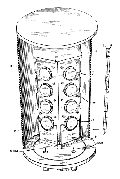
shown in FIG. 1, to have an aluminum tray, 17, with Ardel
outer plates, 18, having cutouts of a size slightly larger
than the individual substrates, contacting grounded
plate, 19. The grounded plate was set off from the driven
electrodes, 20, and pedestals, 21, utilizing Teflon
~78q68
- 1o
insulating spacers, 22. The bell jar, 25, was grounded and
had an internal glass coating that was 0.23cm (0.09 inch)
in thickness. Each substrate position not occupied by a
sample havin~ both a polycrystalline silicon and silicon
dioxide layer was occupied by a silicon substrate covered
with resist to avoid exposure of the aluminum pedestal.
The chamber was evacuated to a pressure of approximately
1.3 x 10 3Pa (1 x 10 5 Torr). A molecular
chlorine flow through the chamber was established at a rate
of 40 sccm. The pumping speed of the vacuum pump was then
decreased so that the pressure in the chamber rose to
approximately 2.67Pa (20 mTorr). An r.f. power of
approximately 70 watts at a frequency of 13.56 M~z was
applied to the driven electrode. The etch rates of the
polycrystalline silicon and silicon dioxide were measured
as described in Example 1. The polycrystalline silicon
etched at a rate of approximately 9.6 nm/minute, the
silicon dioxide etched at a rate of approximately
0.094 nm/minute, and thus the selectivity was approximately
100 to 1. The profiles obtained as the etching reached the
polycrystalline silicon/s~licon dioxide layer interface are
shown in FIG. 5 as an indication of the achieved etch rate
uniormity.
Example 5
The procedure of Example 4 was followed except
the r.f. power was approximately 100 watts, and the bell
jar was entirely a glass composition. A grounded grid of
aluminum enclosed this glass bell jar. The relatively non-
uniform profiles obtained as the etchant reached the
interface between the polycrystalline silicon and silicon
dioxide layers are shown in FIG. 4.
Example 6
The procedure of Example 4 was followed except
the hexagonal cathode was only one tier high, as shown in
FIG. 6, and thus accepted only one substrate per face of
the hexagonal electrode. Additionally, the grounding metal
plate was not present, and only a tray of Ardel, 30,
q876~
1.27cm (0.5 inch) in thickness, surrounding the substrate
and abutting the hexagonal cathode was utilized. The
applied power was 24 watts, and the initially established
chlorine flow rate was 30 sccm. The polycrystalline
silicon etch rate was 23 nm/minute, the silicon dioxide
etch rate was 0.31 nm/minute, and thus the selectivity was
approximately 74 to 1.