Note: Descriptions are shown in the official language in which they were submitted.
` Our Reference: WSU-105-A 1~7~4~ PATENT
THERMAL WAVE IMAGING APPARATUS
BACK(iROUND OF THl~ INVENTION
This invention relate~, in general, to method~ and
devices for non-destructive testing of opaque articles to detect
surface and sub-surface crack~, flaws, voids, etc.
Various methods have been proposed to detect surface and
subsurface cracks, flaws, voids, etc. in opaque solids. One
common method utilizes photo-acoustic techniques in which
periodic, localized heating of a ~ample within a gas-filled cell
is caused by focu~ed inten~ity modulated ligh-tJ electro-magnetic
radiation or a particle beam. The heat generates æound within
the gas medium which are detected by a transducer, such as a
microphone mounted within the gas cell. The transducer or
microphone generates electrical signals which are analyzed to
locate surface and ~ubsurface defects.
In actual use, an argon-ion laser whose output is
modulated is focused onto the surface of interest through an
optical window spaced from the surface of the sample by a ~mall
volume of air vf ga~. The transducer mounted within~the cell
detects the amplitude and phH~e of pressure variations with the
cell caused by the temperature profile at the ~ur-~ace of the
sample. Howevar, while this imaging technique is effective at
detecting certain crack orientations, it cannot detect strictly
vertical, closed cracks. While in practice many cracks are not
quite vertical or not quite closed or both, any cracks which are
strictly vertical and closed would be missed when employing this
technique.
Mirage effect -thermal wave imaging has proven effective
at detecting strictly vertical closed cracks within opsque
solids. This technique~utilizes a laser source -to probe the air
just above the surface of an opaque solid which is heated by a
Z
secon~ modulated laser. ~n ac electrical signal i8 produced by
using a phototransistor to monitor the de~lection of -the probe
beam in a plane parallel or perpendicular to the sample sur-~ace.
Indexing o~ the sample underneath the heating laser beam or
indexing the heating laser beam over -the surface of the sample
results in a series of data signals which are usef~ll in
detec-ting subsurface and surface cracks, flaws, voids and other
defects.
Other imaging techniques currently being used or
investigated include gas cell, photothermal displacement,
infrared detection and piezoelectric detection.
The signals by themselves cannot yield any useEul
in~orma-tion as to the existence of surface or subsurface cracks
without additional analysis. Heretofore, on-line, real time
analysis techniques have been minimal for data generated by the
various thermal wave imaging techniques. This lack o~ useful
date anRlysis techniques has hampered the use of thermal wave
imaging techniques for detecting surface and subsurface cracks
in opaque solid objects.
Thus, it will be desirable to provide an analysis
technique which overcomes the deficiencies in analyzing and
displaying information generated during a thermal wave scan of
opaque solids. It would also be desir~ble to provide an
analysis -technique for use with a thermal wave scan of opaque
solids which generates a vi~ual image of the surface and
immediate subsurface of the solid illustrating any cracks,
flaws, which may exi~t within the solid. ~inally, it would be
desirable to provide an analysis technique for use with thermal
wave imaging of opaque solid~ which generates a visual image
of the exis-tence of any crack~ or flaws within the sample
luring real time when the sampla is being probed by the
thermal wave scan.
%
There is di~closed herein a unique thermsl wave imaging
apparatus which includes unique data acqui~ition features for
genera-ting an on-line, real-time image which is useful in
detecting the presence of any surface or subsurface cracks,
flaws or voids in an opaque solid object.
The -thermal wave imaging apparatus o~ the present
inven-tion can be used with any imaging process including ga~
cell, photothermal displacement, mirage effect, infrared
detec-tion, piezoelectric detection and photoacoustic detection.
By way of example only, the present invention will be described
in use with a mirRge effect imaging apparatus.
As i8 conventional, in the mirage effect technique, a
heating laser generate~ an output which is intensity modulated
to provide a periodic optical signal used to periodically heat a
point on the surface of an object. The optical beam from a
probe laser pa~ses parallel to the surface of the object through
the heated zone. This probe beam i~ deflected from a normal
path due to density variations in the air above the surface of
the sample caused by uneven heating due to the presence of
surface or subsurface cracks, flaws, voids, etc., in the
object. The amount of deflection of the probe beam is detected
to provide an indica-tion of the existence of any surface or
subsurface defects in the object.
According to the present i~vention, the deflection data
are converted to digital signals and stored in an image memory
under the control of a central processor. The stored defection
data are u~ed to control the intensity of poin-ts or pixels on a
display monitor.
Separate means are provided for generating ~equential,
incremental signal~ used to control the X snd Y axis defection
of -the moni-tor. Such signals are also used to address the image
memory and to output the\refrom -the stored data at each address
location corresponding to each generated X and Y deflection datum
to control the intensity of the displayed point or pixel on the
monitor. In this manner, as the ob;ect is probed point by point
across its surface, a real time, on-linP image is generated on
the monitor which provides a visible indication of the presence
of any surface of subsurface cracks, flaws, voids, etc. in the
ob~ect.
The thermal wave imaging apparatus o~ the present
invention also includes a unique feedback circuit which controls
an acousto-optic modulator such that the lntensity or amplltude
of -the heating optical beam directed onto the surface of the
ob~ect remains constant despite any fluctuations or varlations in
the output of the heating laser itself.
Thus according -to the present invention in a thermal
wave imaging apparatus for detecting surface and subsurface
cracks, flaws and voids in opaque solid ob~ects in which A.C.
electrical signals indicative of the configuration of the surface
and subsurface of an opaque, solid ob;ect are generated by a
thermal wave scan of the ob;ect in which a first laser generates
a heating energy ~eam directed through the ob;ect to generate a
surface temperature gradient, a second optical probe beam is
directed through the ob~ect and deflected by the surface
temperature gradient, and means for generating the A.C.
electrical signals indicative of the amount of deflection of the
second optical probe beam, the improvement comprising: means for
converting A.C. electrical signals to digital signals; memory
means for storing the digital signals; central processor means
for controlling the transfer of the digital signals to the memory
means; means for displaying an image of the surface and
subsurface of the ob~ect; and means for generating control
signals for controlling the X and Y axis point deflection of the
displaying means and for addressing the memory means to output
thereErom the digital signals to control the intensity of each
displayed point on the displaying means; modulation means for
modulating the laser output beam to a pulsed beam which strikes
and hats a localizPd point on the object: means for controlling
the amplitude of the output beam from the modulation means, the
means for controlling the amplitude of the optical output beam of
the modulation means comprises- means for detecting the amplitude
of the op-tical beam output from the modulation means; means for
'~ generating an RF slgnal for controlling the modulation means; and
means, responsive to the detecting means, for attenuating the RF
signal so as to control the modulation means such that the output
optical beam from the modulation means remains at a constant
amplitude despite fluctuations in the output optical beam from
the laser.
The thermal wave imaging apparatus of the present
invention overcomes may of the deficiencies of previously devised
1~ techniques for analyzing data generated by the various thermal
wave imaging techniques. The data acquisition apparatus of the
present invention uniquely enables a real time, on-line image to
be generated to provide a visible indication of the presence of
any surface or subsurface cracks, flaws, voids, etc. in the
2~ ob~ect.
The various features, advantages and other uses o the
present invention will become more apparent by referring to the
following detailed description and drawing in which:
Z5
Figure 1 is a pictorial representation of the
temperature profile generated by a mirage effect thermal wave
imaging technique:
Figure 2 is a pictorial representation showing a mlrage
3~ effect thermal wave imaging apparatus;
Figure 3 is a block diagram of the laser beam modulator
and intensity regulation circuit shown in general Figure 2;
3~
- 4a -
8~:
Figure 4 i~ a block diagram showing the data acquisition
and imaging sy~tem of the present invention;
Figure 5 is a detniled ~chematic and block diagra~ of
one data acquisition channel; and
igure 6 is a schematic and block diagram of the image
memory subsystem shown in general in Figure 4.
Throughout the following description and drawing, an
identical reference number is utilized to refer to the same
component shown in multiple figures of the drawing.
The thermal wave imaging apparatu~ of the present
invention i3 configured -to control the acquisition of data
during a thermal wave scan of an opaque solid object and to
; display an image of surface and subsurface of the object 3howing
any cracks, flaws, void or other defects in the surface and
subsurface of the object. The apparatus of the pre~ent
invention may be used with any imaging technique including, but
not limited to, gas cell monitoring, photothermal displacement,
mirage effect detection, infrared detection, photoacoustic and
piezoelectric monitoring. In each o-f these imaging techniques,
ac electrical s:ignals are generated by a detector, such as a
microphone or pho-totransi~tor, which can be analyzed to provide
information about the structure of the object.
By way of example only, the apparatu~ of the present
invention will be de~cribed in conjunction with apparatus for
u~ing the mirage effect thermal wave imaging technique. It will
be understood, however, that the present invention may be
employed with any thermal wave imaging apparatus.
Before describing in detail a preferred construction of
the thermal wave imaging apparatus of the present invention, a
brieE description of the theory behind the mirage effect
; technique for thermal wave imaging will be initially described
to provide a ba~ic understanding of -the principles employed in
~he thermal wave imaging apparatu~ of the prssent invention.
~ ccording to the mirage effect method of thermal wave
imaging, as shown in Figure 1, an optical or laser heating beam
1 is u-tilized -to provide periodic, localized heating of a point
2 on an opaque solid object 3. Such teaching of the object
crea-tes a temperature profile 4 above the surface of the object
in which the density of the air just above and aro~lnd the laser
focal spot varies with tempera-ture variations on the surface
which in turn are influenced by variations in the ~djacent
subsurface of the object. Thus, the presence of cracks, flaws,
voids, on the surface or immediately below the surface of the
object will cause density variations in the air above the
~urface of the object.
A second probe beam passing through this temperature
profile parallel to the surface of the object will be deflected
by such density changes in the air immediately above the surface
of the object 3. Detection of these deflections 6, 7 and 8 of
the second probe beam 5 can be utilized to provide an indication
of the presence of a surface or sub3urface crack, etc.
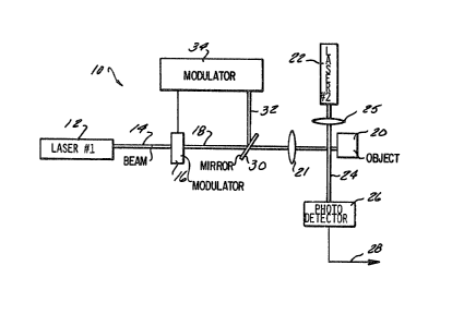
Re~erring now to Figure 2, there is illustrated a
thermal wave imaging apparatus which is constructed to make use
of the mirage effec-t to detect surface and subsurface cracks,
etc., in an opaque solid object. The apparatus 10 include~ 8
first heat source 12, such a8 a laser. Any type of laser 12,
such as an argon-ion laser, may be employed in the apparatu~
10. Furthermore, the la~er 12 may be provided with any power
output and in any wave length. Preferably, however, vi~ible
wave length are employed for ease in aligning and adju3ting the
apparatus 10.
As the laser 12 provides a continuous ou-tput beam 14,
the beam must be perioclically interrupted or modulated to
~Y~7~
provide the desired periodic, localized heating of the objec-t.
Thus, the output beam 14 from the laser 12 i~ pa~sed through Qn
acousto-op-tical chopper or modulator 16, whose output is a
modulated optical bea~ 18. The beam 18 i3 directed onto an
object 20 -through a len~ 21 to cause the de~ired periodic
localized heating of a point on the surface of an opaque, solid
object 20.
A second probe laser 22 i9 oriented such that its output
beam 24 focused by lens 25 passe~ through the heated areQ or
temperature profile generated by the fir~t laser 12 nnd
substantially parallel to the surface of the sample 20. As
noted above, deflections of the output beam 24 caused by density
variations in the air im~ediately above the surface of the
object 20 can be detected by means of a photodetector 26, such
as photodiode array. As is conventional, the photodlode array
26 includes -two pairs of perpendicularly oriented photodiode~.
The diodes in each pair are electrically connected such that an
output signal will be generated on line 28 which will indicate
by means of i-ts magnitude the point on the photodetector 26 on
which the probe beam 24 impirges.
According to one feature of the subject invention, the
thermal wave imaging apparatu3 10 is provided wi-th a feedback
circuit to provide a constant amplitude for the modulated laser
beam 18 despite nny fluctuations or variation~ which may occur
in th0 output beam 14 of the heating laser 12. In effecting
this feedback, Q portion of the optical beam 18 from the modu-
lator 16 is split by means of a conventional beam splitter 30,
such as a partially reflec-tive mirror, which deflects a portion
32 of the optical beam 18 to the feedback circuit 34.
In gener~1, -the beam modulator and intensity regulation
circuit 34 controls the modulator 16 in such a way -that the
amplitude of the output ~eam 18 remains constan-t in~pite of any
342
fluctuations or varia-tions in the intensity of the outpu-t
optical beam 14 generated by the laser 12.
~ s shown in greater detail in Figure 3, the split
portion 32 of the optical beam strikes a photodiode 40 which
generates an electrical output signal proportional to the
intensity or amplitude of the beam 32. The output from the
photodiode 4~ passes -through a low-pass filter circuit 42 to a
gnin control circuit 44. Another input to the gain control
circuit ~4 is a signal from an offset control circuit 46 to
provide reference levels for the feedback signal.
At the same time, a square wave signal 50 at the desired
modulation frequency is fed to a conventional RF switch 54 which
modulates the output signal from a RF ~ignal genera-tor 56. The
amount of RF signal which i3 passed to the modulator 16 is
determined by means of an RF attenuator circuit 58 which
receives the modulated RF signal from the RF switch 54 and the
outpu-t of the gain control 44, with the magnitude o~ the output
of the ~ain control 44 being proportional to the difference
be-tween the output signal from the low-pass filter 4Z and the dc
level of the signal from the offset control ~6. The output of
the attenuator 58 is amplified and fed to the acousto-optic
modulator 16.
The acousto-optic modulator 16 is constructed in a
conventional manner to diffract a portion of the input optical
laser beam 14 into the output beam 18 only when an RF signal is
present. In the ab~ence of an RF signsl as determined by the RF
switch 5~ described above, the output optical beam 18 is
interrupted. In the presence of an RF signal, the intensity of
the output beam 18 is controlled -to a fixed level set by -the dc
offset control 46. In this manner, the intensity of the output
optical beam 18 from the acousto-optic modula-tor 16 remains
z
cons-tant despite any fluctuations or variatlons in the output
optical beam 1~ from the laser 12.
Referrirlg now to Figure 4, there i8 illustra-ted a block
diagram of a data acquisition and contrGl system 80 which
controls the acquisition of d~ta -from the photo- detector 26 and
the generation of a visible image which displays the presence of
any surface cracks, etc., on the object 20. The data
acquisi-tion system 80 is controlled by a central processor unit
82 which can be any conventional microprocessor such HS a
microprocessor sold by Motorola, Model No. 6800. The central
processor 82 functions to control the tran~fer of data between
the various subsystems of the data acquisition system 80 by
genera-ting appropriate timed, control signals. In controlling
such data transfer, the central processor 82 executes a stored
control program shown in Appendix A.
A~ illustratad in Figure 4, the output 2~ from the
photodetector 26 together wit the reference signal 50 is input
to a lock-in amplifier 84 which generates two outputs, one
indicating the magnitude of the output from the photodetector 26
and the other the phase of the output ~ignal from the
photodetec-tor 26 relative to that of the reference signal 50.
Alternately, the two outputs can indicate the in-phase and
quadrature components of the output from the photodiode 26. The
outputs from the amplifier 8~ are input to two separate data
acquisition channels 83 and 86. labeled channel one and channel
two, respectively, corresponding to -the pha~e and magnitude or
the in-phase and quadrature outputs from the photodetector 26.
Only one of the data acqui~ition channels 83 and 85,
such as the firs-t channel 83 corresponding to the magnitude
signal from the photodetector 26, will be described in greater
detail hereafter since both data acquisition channels 83 and 85
are identically construc~ted. As shown in Figure 5, the output
~7~ 2
from the amplifier 84 is input to an ampli*ier 86 whose output
is input to an A~D converter 88.
The A/D converter 88 i~ a~signed to three addres~
locations of the central processor 82, one for starting analog
conver3ion, one for reading the busy state of the A/D con~erter
88 and a third for reading the converted data. In operation,
the central processor 82 initiates a data conversion by sending
a signal on control line 92 to the A/D converter 88, wait~ for a
busy state completion signal on con-trol line 94 -from the A/D
converter 88 and then generate~ a read data signal on control
line 90. The output from the A/D converter 88 is the input on
data bus lines 96 to the central processor 82.
The output data signals from the central processor 82 on
lines 96 are input to two D/A converters 98 aDd 100. Each of
the D/A conv0rters 98 and 100 is assigned a single address and
behaves as a random access memory for the central processor 82.
A number written in the D/A converter 98 is converted into an
analog voltage which is summed by the amplifier 86 with the
analog input signal from the lock-in amplifier 84. This
provides a programmable offset. Control line 104 is the chip
select line and line 106 is the read/write control line for this
operation. In a similar fashion, the D/.A converter 100 provides
a programmable voltage which is input to the A/D converter 88 as
a reference voltage for conversion, thereby providing a
programmable gain control. Control lines 102 and 106 are the
control lin0s for this operation.
Referring again to Figure 4, the output data from the
first data acquisition channel 83 is transferred under the
contro]. of signals generated by the central proce~sor 82 to an
image memory ~ubsystem 110. The image memory subsystem 110
serves as an image memory for a digi-tized microscopic pic-ture of
the objec-t 20. The output of the memory contained with the
image memory subsystem 110 is continuously displayed on a
monitor 112 which, in a pref~rred embodiment, is a high
resolution, -fla-t ~creen display with a linear intensity response
so as to generate a high quality picture suitable for
photography. Furthermore, the data conten-t of the image memory
subsystem 110 is displayed in gray scale on the monitor 112 with
256 di~ferent intensity levels Eor each pixel and a total of
65,536 pixels.
In general, the basic cycle of the central processor 82
is divided into two hslves~ with the central processor 82
addressing memory only during the first half of each cycle.
Then, during the second half of each cycle, the address line~ of
the memory are multiplexed to the output of a 16-bit refresh
counter which is constantly incremented by the CPU clock.
Referring now to Figure 6, there is shown a detailed
block diagram of the image memory subsystem 110. The image
memory subsystem 110 includes a random nccess memory 120 which,
in a preferred embodiment, includes 64~ of 8 bit memory
locations. During each half cycle, the central processor 82
will generate sequential addresses on addre3s bus 122 which are
input to an address multiplexer 12~. The address multiplexer
124 controls the selection of addresses to be used -to address
-the memory 120. During the memory read or write half cycle of
the central processor 82, the address multiplexer 124 will
select addresses -from address bus 122 so as to direct the data
on data bus 96 to the appropriate locations within the memory
120O
As shown in Figure 6, the data bus 96 is also input to a
data line multiplexer 128 which controls the flow of da-ta either
between the central processor 82 and the memory 120 or between
the memory 120 and the D/A converter 144.
8~2
In this manner, data corresponding to the magnitude or
phase o-f the deflection of the probe beam for each sequentially
sampled spot on a surface of -the object 20 i~ stored in
sequential memory locations within the memory 120. The
magnitude or phase of the deflection of the probe beam
corresponds to the intensity of the displayed point image on the
monitor 112. In a preferred embodiment, the two data
acquisition channels 83 and 86 operate in parallel so that both
magn.itude and phase images appear on the monitor 112
simultaneou~ly. Alternately, only one of the channels 83 and 85
may be activa-ted to di~play only a ~ingle image.
The image memory subsystem 110 also includes a control
multiplexer 130 which controls the read-write mode of the memory
lZ0 as well as the selection of addres~e~ by the address
multiplexer 124 and the data multiplexer 128.
A 16-bit refresh counter 140 ~enerotes a new 16-bit
address upon each ENABLE signal from the central processor 82.
The address multiplexer 124 will select the output from the
16-bit counter 140 during each non-read or write h~lf cycle of
the central processor 82. The output of the counter 140 is
input to two D/A converters 142 which convert two 8-bit signals
from the counter 140 to two signals u~ed to control the X and Y
deflection of the monitor llZ. This controls the position of
the next point to be displayed on the monitor 112. At the
same time, the ~ddres~ generated by the counter 140 is input
through the address multiplexer 124 to the memory 120. Data
stored at the ffpecified address location i~ output through -the
data lirle multiplexer 128 to D/A converter 144. The output
signal from the D/A converter 14~ is smplified and fed to the 30 monitor 112 to control the intensity of the point being
displayed on th~ monitor 112.
12
~7~3~342
~ 190 shown in Figure 6 are mode control signals Mo~ M
nnd M2 which are input to gates 146, 148 and 160. The mode
control signals M~, Ml and Mz are generated by the csntral
processor 82 and are used to control the size of the display
image on the monitor 112. For small sample sizes, only one-
eight, one-quarter or one-half of the display screen need be
used. Thus, depending upon -the binary code input on line~ Mo~
Ml and M~ to the 3elected mode control gates 146, 14~ and 150,
onLy one-eighth, one-quarter, one-hal~ or a full screen will
be displayed. When a partial ~creen on the monitor 112 is
displayed, the monitor 112 will be refreshed at a faster rate
which reduces the flickering of the image.
In summary, there has been disclosed a unique thermal
wave imaging apparatus which generates an on-line, real time
image of surface and subsurface crac~s, flaw , etc. OD an opaque
~olid which is probed by means of a thermal wa~e imaging
technique. A laser beam modulation and regulation control
circuit has also been disclosed which generates a modulated
optical beam of a const~nt amplitude or intensity inspite of any
fluctua-tions or variation3 in the output beam of a laser.
s
13